

Page 1

DATASHEET
ENCOUNTER DIGITAL
IMPLEMENTATION SYSTEM
Cadence® Encounter® Digital Implementation System refines
and redefines digital implementation, helping customers deliver
differentiated products to their end market, achieve predictable time
to market with the highest quality silicon, and reduce development
and production costs. It extends the production-proven Encounter
technologies that designers trust to deliver truly scalable, ultraefficient core memory architecture and end-to-end multi-core
parallel processing for the ultimate in capacity and performance. A
comprehensive solution for mainstream and advanced node flat and
hierarchical designs, it addresses the requirements for design closure,
signoff, low power, mixed signal, and manufacturability and yield
optimization.
ENCOUNTER DIGITAL
IMPLEMENTATION
SYSTEM
Encounter Digital Implementation System
provides a focused, high-performance,
advanced design closure solution for both
flat and hierarchical designs while also
addressing the latest requirements for
low-power, mixed-signal, and advanced
node design. By supporting RTL synthesis,
enabling rapid design exploration
and accurate chip feasibility analysis,
full-chip virtual prototyping, and full-chip
digital implementation and signoff in a
single environment, Encounter Digital
Implementation System gives engineers an
early, accurate view of design feasibility
and allows them to progress immediately
to full-scale implementation and final
signoff for large-scale, complex designs—
without ever leaving the solution
environment.
Encounter Digital Implementation System
combines advanced RTL and physical
synthesis, early design exploration
and analysis using black blobs and
automated floorplan synthesis, clock
tree and clock mesh synthesis, advanced
nanometer routing, mixed-signal support,
advanced low-power implementation,
and a complete suite of design-formanufacturability, variation, and yield
optimization technologies required for
advanced node designs. These and other
capabilities enable Encounter Digital
Implementation System to deliver the
highest quality of silicon for timing, signal
integrity, area, power, and yield, including
integrated statistical-based analyses and
optimizations.
BENEFITS
• Predictabilityandconvergence
- Combines the power of RTL
synthesis, early design exploration, full-chip prototyping and
design implementation, and final
signoff analysis in a single unified
environment
- Enables design exploration and
accurate chip feasibility analysis,
including automated floorplan
synthesis and ranking, for a
flexible and predictable path to
design closure
- Supports location-based on-chipvariation technologies and the latest
statistical methodologies including
integrated analysis and optimization
for statistical timing and leakage
• Productivityandfastertimetomarket
- Provides robust and flexible solutions
for hierarchical methodologies,
including bottom-up block-based
flows, top-down black-box flows,
and hybrid flows with partitioning,
time budgeting, and innovative
top-level assembly and optimization
technologies
- Delivers signoff-driven implementation and intuitive and visual global
timing, power, and clock debug and
diagnostics features
Page 2
• Scalabilityinperformance
- Delivers industry-leading performance
and capacity for large, complex chips
- Offers a complete, end-to-end, multicore parallel processing backplane
and infrastructure
• Differentiatedproductdevelopment
with lower production costs
- Provides a comprehensive and
tapeout-proven solution for complex
design closure, low-power, mixedsignal, and advanced node design
implementation and optimization
- Supports comprehensive
multi-mode/multi-corner analysis
and optimization in all steps across
the design flow
- Enables concurrent chip/package
design and optimization with
integrated capabilities such as
automatic area and peripheral I/O
placement and optimization, and
flip-chip RDL routing
- Allows floorplanning, implementation, and analysis of stacked die
in 3D IC
DESIGN CLOSURE
Encounter Digital Implementation System
supports all implementation styles—from
flat or hierarchical to single or multiVDD. The fast power-grid design and
optimization, global routing, in-place
optimization, and global timing debug
capabilities provide a robust infrastructure
to implement any methodology.
EARLY DESIGN EXPLORATION
Today’s physical design teams start
physical implementation and design
planning very early in the design cycle—
with early and multiple versions of the
design netlist—to determine design
feasibility. Among the questions needing
answers are the following: Can the design
be implemented in the required area? Can
the design operate at the desired speed?
Does it meet power requirements?
l
a
I
m
t
i
p
g
i
D
r
e
t
n
u
n
o
c
n
E
t
u
o
R
r
e
t
e
m
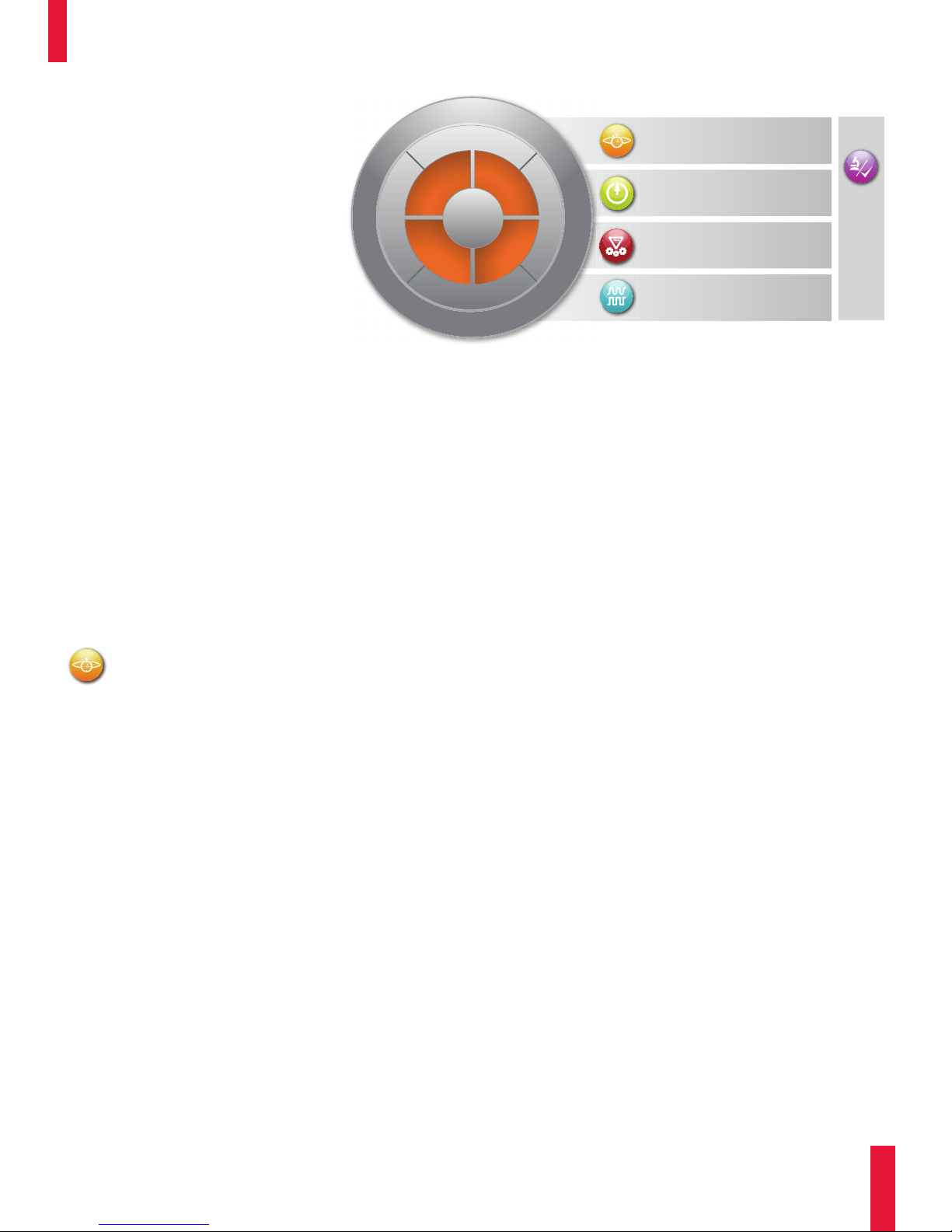
Figure 1: Encounter Digital Implementation System delivers a comprehensive solution
i
n
n
a
l
P
S
o
Q
g
/
n
a
i
e
r
A
Design
Closure
P
r
o
o
d
n
u
a
c
t
N
i
v
i
t
S
i
g
n
o
Encounter Digital Implementation System
addresses these challenges:
• Production-provenautomatedoorplan
synthesis of Cadence First Encounter®
technology closes the gap between
the architecture and implementation
by enabling timing, power, area, and
congestion-aware placement coupled
with fast global routing and in-place
optimization; helps designers quickly
generate prototype floorplans
l
e
m
e
n
t
r
o
P
/
t
o
g
t
P
r
e
e
y
P
l
a
f
n
f
A
a
y
d
r
y
t
p
i
i
n
o
g
n
i
P
c
t
h
a
y
b
s
i
l
i
i
c
t
a
y
l
S
y
n
e
t
c
h
n
e
s
a
i
s
m
r
o
f
s
i
s
Large Chip Design Closure
Low-Power Design
Advanced Node Design
Mixed-Signal Design
Encounter Silicon Virtual Prototyping to
bring physical predictability into their
estimations
SILICON VIRTUAL PROTOTYPING
AND HIERARCHICAL CAPABILITIES
Full-chip flat prototyping delivers the
complete physical, timing, clock, and
power data, thereby eliminating the
guesswork associated with traditional
block-based approaches. Hierarchical
support helps physical designers assess
• Built-inexibilityandeditingcapabilities
such as relative floorplan (specifying
relationships for pre-routes, resizable
objects, multiple relations, datapath
stacking, and integrated analysis tools)
and resize floorplan; enable designers
to quickly and accurately reach an
optimal final floorplan
• Floorplanrankingsystemautomatically
generates multiple floorplan scenarios
in parallel and analyzes them based on
pre-defined quality-of-results criteria;
allows designers to explore as much of
the physical solution space as possible
and make the most informed tradeoff
for design feasibility
• Uniqueabstractionmodels(black
blobs) enable very early and fast
design planning for huge designs;
allows designers to start the design
planning process even when no netlist
is available; also enables a path where
system designers can use Cadence
InCyte Chip Estimator and link it to First
how best to partition the logical hierarchy
into physical modules. With hierarchical
support, designers can analyze the
optimal pin assignments, budget time
quickly, accurately predict the clock
distribution networks, analyze the power
grids, and eventually generate complete
timing and physical constraints for each of
the physical modules.
ADVANCED TIMING CLOSURE
Encounter Digital Implementation
System’s global physical synthesis
capability optimizes multiple paths
simultaneously while performing multidimensional and concurrent optimization
for timing, signal integrity, power, area,
congestion, wire length, and yield using
native signoff engines in the process.
Additionally, significant improvements in
performance, accuracy, and throughput
can be achieved using robust end-to-end
multi-mode/multi-corner (MMMC) analysis
and optimization technologies.
Signoff Analysis
www.c a den c e.c om
ENC OU NTER DI GI TAL I MPLE MEN TAT ION S YSTE M
2
Page 3

With its patented architecture, SMART2
routing technology (concurrent signal
integrity, manufacturing-aware,
routability, and timing optimization),
litho-aware routing, and the industry’s
only superthreading technology, Cadence
NanoRoute® Advanced Digital Router is
unmatched in quality and performance
for block-level and top-level routing. It
simultaneously addresses multiple design
objectives for the ultimate DRC-clean
tapeout-ready GDSII database.
NanoRoute Router further extends its
leading grid- and graph-based routing
and optimization technologies to support
the latest 45- and 32-nanometer design
rules. It delivers a full suite of design-foryield (DFY) features including concurrent
via-doubling and reduction, wire
spreading and widening, variation control,
and lithography hotspot prevention
and optimization. Finally, NanoRoute
superthreading technology combines
the best of multi-threading, multi-core,
and parallel-processing techniques. This
enables designers to route millions of
nets per hour on both readily available
and cost-effective 32-bit compute
technologies and the latest developments
in multi-core processing hardware.
ADVANCED GLOBAL DEBUG AND
DIAGNOSTICS
Debug and diagnosis challenges often
come late in the design cycle, along
the critical path toward reaching
final tapeout. Encounter Digital
Implementation System timing, power,
and clock debug and diagnostics
capabilities provide significant advantage
by enabling designers to quickly zero in
on and visualize interdependent timing,
clock, and power issues, then quickly
resolve them using powerful “what-if”
analysis techniques—with results that
can be immediately implemented in
physical design.
ADVANCED RTL SYNTHESIS
RTL synthesis for high-performance
systems requires not only high
capacity but also advanced features
to optimize the design. Encounter
Digital Implementation System supports
register retiming, accurate physical
layout prediction, multi-supply voltage
(MSV)-aware synthesis, and other features
to achieve high quality of silicon (QoS).
Its integrated and physically-aware
synthesis technology enables designers
to dramatically improve gate-level netlists
derived from other synthesis tools,
resulting in superior timing, area, and
power.
CONCURRENT CHIP/PACKAGE
DESIGN: FLIP-CHIP SUPPORT
Encounter Digital Implementation
System flip-chip floorplanning and
implementation technologies enable
the concurrent design of chip and
package by including package constraints
and parasitic effects while designing
the IC. With support for multiple I/O
methodologies, concurrent optimization
of area and peripheral I/Os with core
instances, automatic RDL routing with
45-degree support, and accounting for
RDL layers during signal/power routing,
Encounter Digital Implementation System
eliminates the traditional manual steps
in I/O placement and optimization. This
mature technology has been proven
through multiple customer tapeouts.
SIGNOFF ANALYSIS
Successful digital chip design hinges
on accurate and consistent signoff
analysis. By integrating with Encounter
Power System, Encounter Timing
System, and Cadence QRC Extraction,
Encounter Digital Implementation System
addresses logical, physical, electrical, and
manufacturing domain requirements
in a single, easy-to-use environment.
This enables convergent front-end to
back-end design handoff, signoff-driven
implementation, and highly accurate final
chip signoff that analyzes chip timing,
signal integrity (SI), power consumption,
statistical static timing, electromigration,
and thermal characteristics.
The integrated signoff solution enables:
• Industry-endorsedandsilicon-proven
timing, noise, and power analysis
during implementation and signoff
• Consistentsignoffanalysesand
extraction between implementation
in Encounter Digital Implementation
System and signoff in Encounter
Timing and Power Systems, as well
as QRC extraction, for faster design
convergence
• Multi-dimensionalroot-causeanalysis
for power and timing that shaves weeks
off of tapeout schedules and prevents
silicon failures
• Fastestturnaroundtimeforincremental or ECO extraction with built-in
integrated QRC extraction
• Theindustry’smostpreciseSIanalysis
for reduced crosstalk noise margins
• High-throughput,multi-coreparallel
processing architecture with truly
concurrent multi-mode/multi-corner
analysis
• Earlyrailanalysisandpower-switch
optimization leveraging Encounter
Power System for highly optimized,
correct-by-construction power
network design
• Staticanddynamicpowerrailanalysis
with IR-drop and clock-jitter impact
on timing
• Variation-aware,statisticaltiming
and leakage power analysis with
effective current source model support
for greater accuracy at advanced
process nodes
www.c a den c e.c om
ENC OU NTER DI GI TAL I MPLE MEN TAT ION S YSTE M
3
Page 4

ADVANCED NODE
DESIGN
ADVANCED PROCESS VARIATION
SUPPORT
Variations in manufacturing can result
in structural changes in devices and
interconnect, leading to deviations
in their electrical behavior. At 65nm
and below, process control becomes
significantly more challenging, leading
to a larger variation as a percentage of
the total size of the design’s features.
As a result, designs that pass traditional
signoff standards might still fail in silicon
due to process variations. In addition
to providing foundry supported signoff
technologies for timing, SI, and power
during implementation, Encounter Digital
Implementation System employs locationbased on-chip variation (LOCV), which
uses logic level and physical location to
select the optimal de-rating factor. LOCV
eliminates the excessive guardbanding
associated with traditional de-rating and
improves timing closure.
Encounter Digital Implementation System
also supplements traditional singleand multi-corner–based methods with
powerful and accurate statistical static
timing analysis (SSTA) that accurately
accounts for variability of process
parameters in a single run. Using effective
current source models (ECSMs), Encounter
Digital Implementation System identifies
cells and nets on both clock and data
paths that are sensitive to variations,
and then determines the probability of
timing failures over the full scope of the
process window. This reduces pessimism
and limits guardbanding, which results in
decreased area and power consumption
while improving chip performance.
Encounter Digital Implementation System
SSTA and statistical leakage analysis and
optimization capabilities further reduce
design cycles by eliminating the need
for multiple analysis runs. Designers can
tape out with the confidence of using
a foundry-endorsed statistical solution
to achieve and improve their timing and
power goals in silicon.
DESIGN FOR YIELD
Yield presents one of the biggest
challenges at advanced process nodes,
especially for high-performance designs.
Encounter Digital Implementation System
optimizes yield issues all the way from
RTL to GDSII. At any point in the design
flow, designers can perform yield analysis,
analyze multiple strategies that can
affect and improve yield, and optimize
the design immediately in the context
of all other optimization objectives
including timing, SI, power, and area. Key
design-for-yield (DFY) features include
wire-spreading, wire-widening, double-cut
via insertion, single via reduction and
optimization, critical area analysis and
optimization, true lithography distortion
prevention and optimization, CMP-aware
metal fill, and a rich set of random and
systematic visual analysis and text-based
reporting vehicles. Encounter Digital
Implementation System’s robust native
DFY capabilities allow designers to quickly
and accurately predict manufacturing
variability and to make intelligent
tradeoffs during prototyping and
implementation for maximizing yield.
DESIGN FOR MANUFACTURING
At advanced nodes, the widening
lithography manufacturing gap and
growing complexity lead to a dramatic
increase in design rules and potential litho
hotspots. The sequential communication
between the router and the signoff litho
analysis tools that helped at older nodes
becomes a bottleneck at advanced nodes,
as it affects the overall design cycle time.
Encounter Digital Implementation System
leads the industry in advanced node
enablement with the new Encounter
DFM, which is more than 100 times faster
than design-side litho signoff analysis
tools. It leverages the foundry-qualified
litho model and aggressive filtering, and
then screens the design during routing for
potential areas that could fail on silicon.
Litho hotspots identified are automatically
fixed using NanoRoute technology.
This novel approach is the first in the
EDA industry and provides designers a
convergent litho hotspot elimination
flow that follows the core principles of
prevention, optimization, analysis, and
signoff to deliver “correct by design”
results.
LOW-POWER
DESIGN
Design teams constantly strive to reduce
power consumption at the chip or systems
level to become and remain competitive
in today’s industry. However, power must
be considered with other design goals
in a simultaneous and multi-objective
optimization approach. Encounter Digital
Implementation System is an integral
part of the Cadence Low-Power Solution,
which provides a complete design-tosignoff methodology. It begins with early
design planning and system architecture
then continues through front-end design,
functional verification, synthesis, physical
implementation, packaging, and signoff.
Encounter Digital Implementation
System’s underlying infrastructure
simplifies the implementation of
low-power designs because it is multiple
power domain–aware across the flow.
Floorplanning, placement, clock tree
synthesis, optimization, routing, analysis,
and all other steps in the design flow
comprehend and optimize across all
power domains simultaneously. The
native integration of complete multisupply voltage (MSV) management also
enables automatic placement of level
shifters with all power connections
completed automatically. This enables
the implementation of designs that
employ power reduction techniques
such as power shutoff (PSO), MSV,
dynamic voltage/frequency scaling (DVFS),
substrate biasing, and many more.
Encounter Digital Implementation System
also fully supports the Common Power
Format (CPF) specification for advanced
power reduction techniques, from
design and verification through final
implementation and signoff.
www.c a den c e.c om
ENC OU NTER DI GI TAL I MPLE MEN TAT ION S YSTE M
4
Page 5

MIXED-SIGNAL
DESIGN
Mixed-signal design and physical
implementation are increasingly
challenging. The amount of analog
circuitry on SoCs is multiplying, and at the
same time, the use of digital control logic
is growing inside analog blocks. The result
is blurred boundaries between “analog”
and “digital.”
The Cadence Mixed-Signal Solution,
utilizing OpenAccess as a single design
database, enables analog and digital
design engineers to retain their own
preferred design environments while
increasing implementation efficiency
through easy and seamless data transfer
between Virtuoso® and Encounter design
platforms. Both analog and digital teams
can easily see the complete design and
any changes that might have been
implemented by their peers, enabling
efficient full-chip optimizations that were
previously unobtainable.
The additional interoperability has proven
extremely valuable during design stages
where both analog and digital design
teams need to carefully coordinate and
agree on potential modifications, where
simply saving the database enables
everyone on the design team to see the
latest status in their own environment.
Engineering change orders (ECOs) can be
managed more easily since they no longer
require the generation of LEF/DEF/GDSII
files to communicate the changes.
Comprehensive full-chip static timing
analysis has always been challenging for
mixed-signal designs, typically because the
custom/analog design engineers had to
manually create Liberty (.lib) files for their
completed mixed-signal blocks. Encounter
Digital Implementation System has a
unique ability to perform comprehensive
static timing analysis by transcending the
analog hierarchy and extracting the digital
logic and paths.
The Cadence Mixed-Signal Solution
combines all of the strengths of Encounter
Digital Implementation System, including
design closure, signoff analysis, advanced
node design, and low-power design with
the industry-standard Virtuoso design
platform for custom/analog design,
enabling a mixed-signal implementation
solution that is second to none.
PLATFORMS
• lnx86:Linux(x86andx86_64)32/64bit
• sol86:Solaris(x86_64)64bit
• sun4v:Solaris(ultraSparc)64bit
• ibmrs:AIX(power)64bit
CADENCE SERVICES AND
SUPPORT
• Cadenceapplicationengineerscan
answer your technical questions by
telephone, email, or Internet—they can
also provide technical assistance and
custom training
• Cadencecertiedinstructorsteach
more than 70 courses and bring
their real-world experience into the
classroom
• Morethan25InternetLearningSeries
(iLS) online courses allow you the
flexibility of training at your own
computer via the Internet
•CadenceOnlineSupportgivesyou
24x7 online access to a knowledgebase
of the latest solutions, technical
documentation, software downloads,
and more
For more information
contact Cadence sales at:
+1.408.943.1234
or log on to:
www.cadence.com/
contact_us
© 2010 Cadence Design Systems, Inc. All rights reserved. Cadence, the Cadence l ogo, Enco unter, First Encounter, NanoRoute, and Virtuoso are registered
trademarks of Cadence Design Systems, Inc. All others are properties o f their r espective holders.
21288 12/09 MK/DM/PDF
 Loading...