

Page 1
DATASHEETDATASHEET
ALLEGRO FPGA
SYSTEM PLANNER
The Cadence® Allegro® FPGA System Planner addresses the
challenges that engineers encounter when designing one or
more large-pin-count FPGAs on the PCB board—which includes
creating the initial pin assignment, integrating with the schematic, and ensuring that the device is routable on the board.
It delivers a complete, scalable technology for FPGA-PCB
co-design that automates creation of optimum “device-rulesaccurate” pin assignment. By replacing manual, error-prone
processes with automatic pin assignment synthesis, this unique
placement-aware solution eliminates unnecessary physical
design iterations while shortening the time required to create
optimum pin assignment.
Cadence FPGA System Planner
technologies are available in the
following product offerings:
• Allegro FPGA System Planner L,
XL, and GXL
• Allegro FPGA System Planner Two
FPGA Option L
• Cadence OrCAD FPGA System
Planner
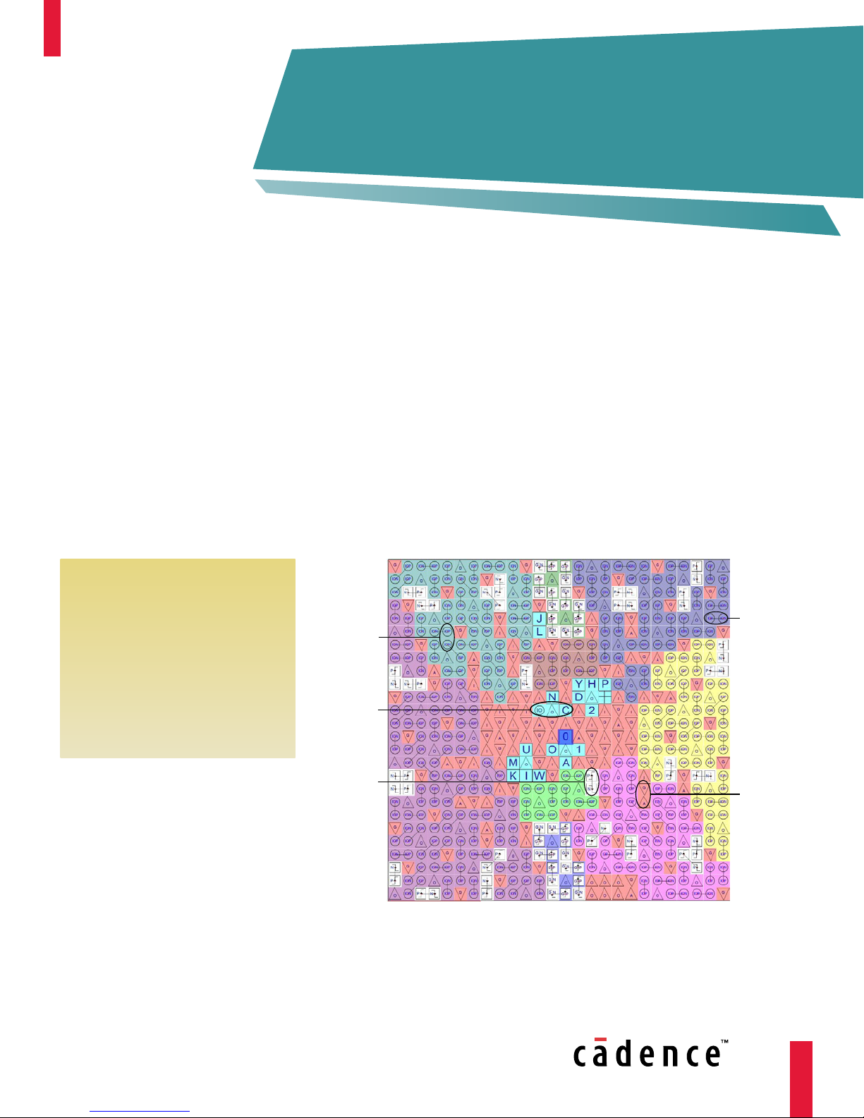
User IO
Configurable
Clock
Capable
Figure 1: Color-coded map of the I/Os of a multi-bank FPGA with different types of configurable pins
Differential
Power
Page 2
DESIGNING LARGE-PINCOUNT FPGAS ON PCBS
Integrating today’s FPGAs—with their
many different types of assignment rules
and user-configurable pins—on PCBs is
time consuming and extends design cycles.
Often the pin assignment for these FPGAs
is done manually at a pin-by-pin level in
an environment that is unaware of the
placement of critical PCB components
that are connected to FPGAs. Without
understanding the impact to PCB routing,
FPGA-based design projects are forced to
choose between two poor options: live
with suboptimal pin assignment, which
can increase the number of layers on a PCB
design; or deal with several unnecessary
iterations at the tail end of the design cycle.
Even with several iterations, this manual
and error-prone approach can result in
unnecessary PCB design re-spins.
With the added time required to generate
pin assignments for FPGAs using manual
approaches, users are unable to do tradeoffs between the different FPGA devices
available and the cost of devices used
in an FPGA sub-system. This is because
performing the trade-offs would mean
that users would have to do two projects
in parallel with no design reuse of any
kind between the two.
With a way to quickly synthesize optimum
pin assignment using user-specified design
intent at a high-level, the Allegro FPGA
System Planner enables designers to explore
their FPGA-based architecture and to create
an optimum correct-by-construction pin
assignment for either production or
prototype designs that use FPGAs.
The Allegro FPGA System Planner is
integrated with the Cadence design
creation tools: Cadence OrCAD
and Cadence Allegro Design Entry (CIS
and HDL). It reads and creates schematic
symbols for both OrCAD Capture and
Allegro Design Entry HDL. In addition,
a floorplan view uses existing footprint
libraries for OrCAD PCB Designer and
Allegro PCB Editor. Should placement
change during layout, pin optimization
using the Allegro FPGA System Planner
can be accessed directly from the Allegro
PCB Editor.
®
Capture
BENEFITS
• Scalable,cost-effectiveFPGA-PCB
co-design solution from OrCAD Capture
to Allegro GXL
• Shortenstimeforoptimuminitialpin
assignment, accelerating PCB design
schedules
• AcceleratesintegrationofFPGAswith
Cadence PCB design creation
environments
• Eliminatesunnecessary,frustrating
design iterations during the PCB layout
process
• Eliminatesunnecessaryphysical
prototype iterations due to FPGA pin
assignment errors
• ReducesPCBlayercountthrough
placement aware pin assignment and
optimization
FEATURES
ALLEGRO FPGA SYSTEM PLANNER
TECHNOLOGY
An FPGA system is defined as a subset of
the PCB design that includes one or more
FPGA and non-FPGA components that are
connected to FPGAs.
Traditional approaches to pin assignment
are typically manual and often based on
a spreadsheet. Tools such as these require
users to do pin assignment without
taking into consideration the placement
of other components and routability
of the interfaces and signals. Above
all, there is no online rules-checking to
ensure that the right pin types are being
The Allegro FPGA System Planner
provides a complete, scalable solution
for FPGA-PCB co-design that allows
users to create an optimum correct-byconstruction pin assignment. FPGA pin
assignment is synthesized automatically
based on user-specified, interface-based
connectivity (design intent), as well as
FPGA pin assignment rules (FPGA-rules),
and actual placement of FPGAs on PCB
(relative placement). With automatic pin
assignment synthesis, users avoid manual
error-prone processes while shortening
the time to create initial pin assignment
that accounts for FPGA placement on the
PCB (placement-aware pin assignment
synthesis). This unique placement-aware
pin assignment approach eliminates
unnecessary physical design iterations that
are inherent in manual approaches.
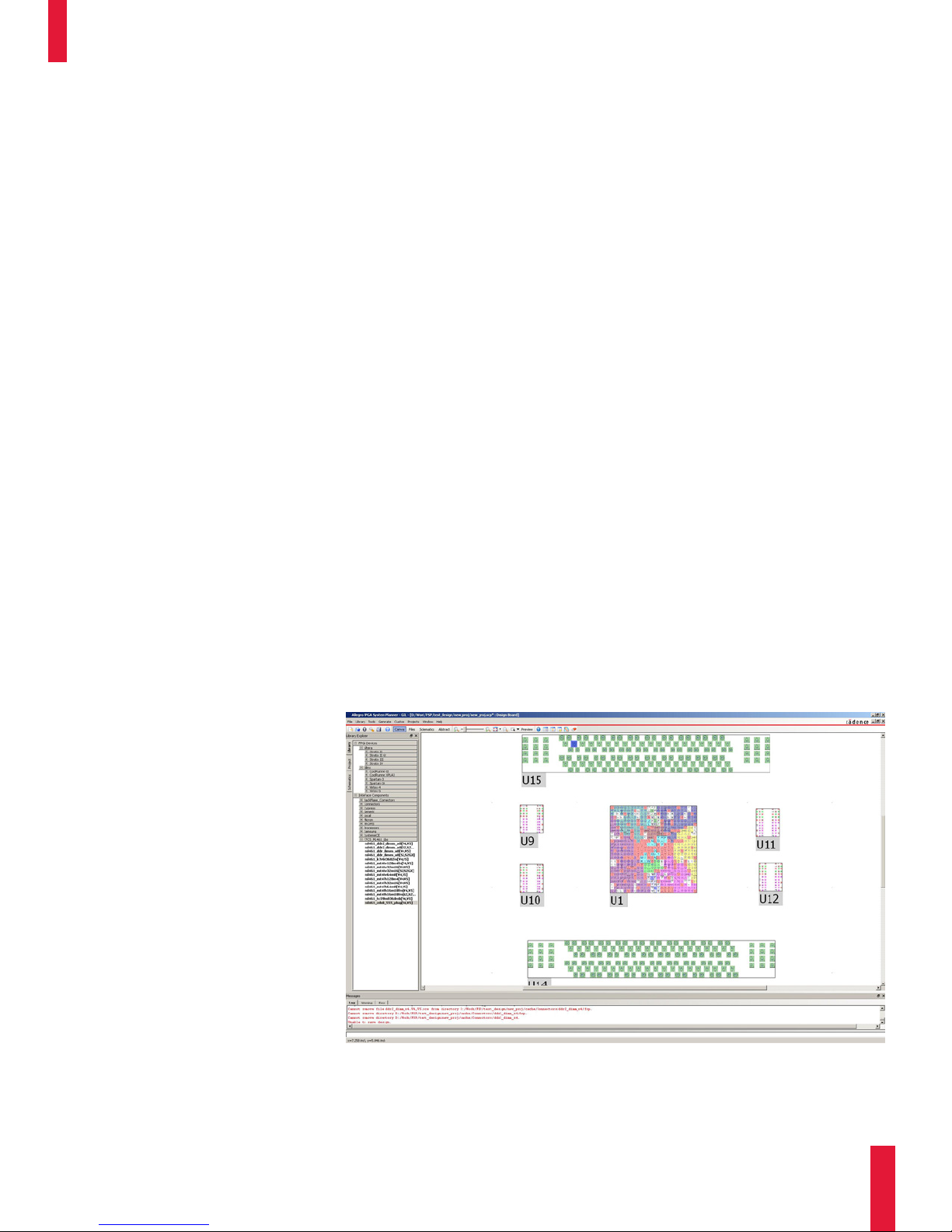
Figure 2: Placement/Floorplan view of the Allegro FPGA System Planner provides users relative placement of
critical components for optimum pin assignment synthesis
www.c a den c e.c om
CAD EN CE A LLE GR O FP GA SY STEM PL AN NER
2
Page 3

FPGA
Vendor
Tools
Allegro
FPGA
System Planner
Allegro
Design
Entry
Allegro
PCB
Design
definitions. Users can create interfaces
such as DDR2, DDR3, and PCI Express,
and use these to specify connectivity
between a FPGA and a memory DIMM
module or between two FPGAs. The
Allegro FPGA System Planner understands
differential signals, and power signals, as
well as clock signals.
Allegro
Part Library
Symbols, Footprints
Figure 3: The Allegro FPGA System Planner uses symbols and footprints from existing libraries
used for the signals that are assigned to
the FPGA pins. As a result, users have
to make several iterations between the
spreadsheet-based tools and the tools
from FPGA vendors. Often this adds an
increased number of iterations between
the PCB layout designer who cannot
route the signals from FPGA pins on
available layers and the FPGA designer
who has to accept paper-based or verbal
pin-assignment suggestions from the
PCB layout designer. Once a change is
made to the pin assignment by the FPGA
SPECIFYING DESIGN INTENT
The Allegro FPGA System Planner comes
with an FPGA device library to help with
selection of devices to be placed. It uses
OrCAD PCB Designer or Allegro PCB Editor
footprints for the floorplan view and allows
users to quickly create relative placement
of the FPGA system components.
The Allegro FPGA System Planner allows
users to specify connectivity between
components within the FPGA sub-system
at a higher level through interface
designer, the pin assignment change has
to be made in the schematic design by
the hardware designer. Such iterations
add several days if not weeks to the
design cycle and possibly a great deal of
frustration for the team members. Since
this is a manual process, mistakes that
are not detected can also cause expensive
physical prototype iterations.
FPGA DEVICE RULES
The Allegro FPGA System Planner comes
with a library of device-accurate FPGA
models that incorporate pin assignment
rules and electrical rules specified by FPGA
device vendors. These FPGA models are
used by the synthesis engine to ensure
that the vendor-defined electrical usage
rules of the FPGAs are strictly adhered
to. These rules dictate such things as
clock and clock region selection, bank
allocation, SSO budgeting, buffer driver
utilization, I/O standard voltage reference
levels, etc. During synthesis, the Allegro
FPGA System Planner automatically checks
hundreds of combinations of these rules
to ensure that the FPGA pins are optimally
and accurately utilized.
While it may help to automate the
synchronization of changes made to the
pin assignment by the FPGA designer,
hardware designer, or PCB layout
designer, it doesn’t reduce the root cause
of these iterations. Pin assignment that
is not guided by all three aspects—FPGA
resource availability, FPGA vendor pin
assignment rules, and routability of FPGA
pins on a PCB—requires many iterations
at the tail end of the design process,
thereby extending the time it takes to
integrate today’s complex, large-pin-count
FPGAs on a PCB.
www.c a den c e.c om
Figure 4: The Allegro FPGA System Planner optimizes multiple FPGAs concurrently
CAD EN CE A LLE GR O FP GA SY STEM PL AN NER
3
Page 4

PLACEMENT AWARE PIN
ASSIGNMENT SYNTHESIS
The Allegro FPGA System Planner
provides users a way to create an FPGA
system placement view using Allegro
PCB footprints. Users specify connectivity
between components in the placement
view and the FPGA at a high level using
interfaces such as DDRx, PCI Express, SATA,
Front Side Bus, etc. that connect FPGAs
and other components in the design,
shortening the time to specify design
intent for the FPGA system.
Once the connectivity of the FPGA to
other components in the sub-system is
defined, the Allegro FPGA System Planner
then synthesizes the pin assignment based
on the user’s design intent, available FPGA
resources, component placement around
the FPGA, and the FPGA vendor’s pin
assignment rules.
The Allegro FPGA System Planner has
a built-in DRC engine that incorporates
the rules provided by FPGA vendors for
pin assignment, reference voltages, and
terminations. This rules-based engine
prevents PCB physical prototype iterations
as the FPGAs are always correctly
connected.
Pin assignment algorithms are optimized
to assign interface signals to a group of
pins, thereby minimizing net crossovers
and improving routability on the PCB.
ARCHITECTURAL EXPLORATION
ENABLED
During the device selection process,
FPGA designers need a way to evaluate if
the FPGA(s) they choose can meet their
application needs while keeping the cost
of devices as low as possible. Estimating
FPGA resource requirements can be
tricky and requires designers to balance
Look Up Tables (LUTs), high-speed I/O
requirements, and memory with I/Os for
low-speed signals. Sometimes choosing
more than one FPGA may be cheaper
than choosing one large FPGA. While
at other times choosing an FPGA with
a larger pin count will suffice, thereby
saving board space and routing channels.
Manual pin assignment approaches make
performing these cost and performance
trade-offs very time consuming and
tedious. With its placement-aware FPGA
I/O pin assignment synthesis, the Allegro
FPGA System Planner helps designers do
trade-offs quickly, enabling architectural
exploration that is not practical with
manual approaches.
ASIC PROTOTYPING USING FPGAS
Some companies choose to do ASIC
prototyping using FPGAs on the PCB. In
these cases, the number of FPGAs used
grows rapidly. This sometimes requires
using several PCBs to place all the FPGAs.
With a large number of FPGAs, the time
to do initial pin assignment can be very
long using manual processes. Additionally,
without taking placement of these FPGAs
into account, the pin assignment can make
routing of the PCB a very long process,
extending the time it takes for designers to
get to the ASIC prototype using FPGAs.
The Allegro FPGA System Planner shortens
the time required to create pin assignment
for a large number of FPGAs through
placement-aware pin assignment synthesis
that is driven by a device-accurate FPGA
models library. With the ability to export
port information in Verilog
Verilog-based connectivity, the Allegro FPGA
System Planner allows users to iterate with
RTL partitioning software, shortening the
time to define the FPGA-based system and
quickly creating DRC-accurate FPGA pin
assignment.
®
and import
Concurrent device
optimization
Placement-aware
synthesis
Reuse symbols
and footprints
Symbols &
schematic
generation
Post-placement
optimization
Schematic power
connections
Schematic
terminations
www.c a den c e.c om
OrCAD FPGA
System Planner
Allegro FPGA
System Planner L
Allegro FPGA
System Planner
Two FPGA Option
Allegro FPGA
System Planner XL
Allegro FPGA
System Planner
1 FPGA 1 FPGA 2 FPGAs 4 FPGAs Unlimited FPGAs
Yes Yes Yes Yes Yes
Yes Yes Yes Yes Yes
Allegro Design Entry
CIS / Allegro Design
Entry HDL
OrCAD Capture
Allegro Design Entry
CIS / Allegro Design
Entry HDL
Allegro Design Entry
CIS / Allegro Design
Entry HDL
Allegro Design Entry
CIS / Allegro Design
Entry HDL
No Yes Yes Yes Yes
No Yes Yes Yes Yes
No Yes Yes Yes Yes
CAD EN CE A LLE GR O FP GA SY STEM PL AN NER
GXL
4
Page 5

TIGHT INTEGRATION WITH
CADENCE DESIGN CREATION
The Allegro FPGA System Planner
generates Allegro Design Entry CIS and
Allegro Design Entry HDL schematics for
the FPGA sub-system. It uses existing
symbols for FPGA in Allegro Design Entry
symbol libraries. If the user desires, the
Allegro FPGA System Planner can create
split symbols for FPGA based on the
connectivity or one split symbol per bank.
INTEGRATION WITH FPGA
VENDOR TOOLS
In addition to integration with Cadence
PCB design tools, the Allegro FPGA System
Planner communicates seamlessly with
FPGA design tools. It generates and reads
supported FPGA vendors’ pin assignment
constraint files. This capability enables the
FPGA designer to evaluate pin assignments
against the functional needs of the FPGA.
Any changes made by the FPGA designer
to account for these requirements can be
imported into the Allegro FPGA System
Planner so that the complete set of pin
assignments remain in sync.
PRE-ROUTE PIN ASSIGNMENT
OPTIMIZATION
The initial pin assignment—that accounts
for placement and routability of the
FPGA on a PCB—goes a long way toward
reducing costly design iterations between
FPGA designer, PCB layout designer, and
hardware designer. Once the PCB layout
designer starts to plan the routing of
interfaces and signals on FPGA, it is possible
to further refine the FPGA pin assignment
based on route intent, layer constraints,
and fanout chosen for the FPGA. The
Allegro FPGA System Planner offers users
a way to optimize FPGA pin assignment
after placement and during routing of the
interfaces and signals on a FPGA.
SCALABILITY
The Allegro FPGA System Planner
technology is available in the following
product offerings:
• AllegroFPGASystemPlannerGXL—for
synthesizing and optimizing pin
assignment of more than four FPGAs at
a time. Suitable for companies that use
FPGAs to prototype ASICs
• AllegroFPGASystemPlannerXL—for
concurrent pin assignment, synthesis,
and post-placement optimization of up
to four FPGAs at a time
• AllegroFPGASystemPlannerL—forpin
assignment synthesis and post-placement
optimization of a single FPGA
• OrCADFPGASystemPlanner—for
optimum initial pin assignment
synthesis of a single FPGA.
OPERATING SYSTEM
SUPPORT
ALLEGRO PLATFORM
TECHNOLOGY
• Linux
• Windows
OrCAD TECHNOLOGY
• Windows
CADENCE SERVICES AND
SUPPORT
• Cadenceapplicationengineerscan
answer your technical questions by
telephone, email, or Internet; they can
also provide technical assistance and
custom training.
• Cadencecertiedinstructorsteach
more than 70 courses and bring their
real-worldexperienceintothe
classroom.
• Morethan25InternetLearningSeries
(iLS) online courses allow you the
exibilityoftrainingatyourown
computer via the Internet.
• SourceLink
gives you answers to your technical
questions—24hoursaday,7daysa
week—includingthelatestinquarterly
software rollups, product change
release information, technical
documentation, solutions, software
updates, and more.
®
online customer support
© 2009 Cadence Design Systems, Inc. All rights reserved. Cadence, the Cadence l ogo, Alle gro, OrCA D, Source Link, and Verilog ar e registe red trade marks of Cadence
Design Systems, Inc. All others are properties of their respective hol ders.
20889 06/09 KM/MVC/DM/PDF
For more information
contact Cadence sales at:
+1.408.943.1234
or log on to:
www.cadence.com/
contact_us
 Loading...