


Manual P/N 854-11001 BVM Limited,
Hobb Lane,
Hedge End,
Southampton,
SO30 0GH, UK.
TEL: +44 (0)1489 780144
FAX: +44 (0)1489 783589
E-MAIL: sales@bvmltd.co.uk
WEB: http://www.bvmltd.co.uk
User's Manual
PMCCTR32
32-bit Opto-Isolated I/O
Counter/Timer PMC Module
Board Revision B
Manual Revision A 06 April 2001
This material contains information of proprietary interest to BVM Ltd. It has been supplied in
confidence and the recipient, by accepting this material, agrees that the subject matter will not be
copied or reproduced, in whole or in part, nor its contents r evealed in any manner or to any person
except to meet the purposes for which it was delivered.

This page is intentionally left blank.

i
DISCLAIMER
The information in this document has been checked and
is believed to be entirely reliable, however no
responsibility is assumed for inaccuracies. BVM Ltd.
reserves the right to make changes and/ or improvements
in both the product and the product documentation without
notice. BVM Ltd. does not as sume any liability arising out
of the application or use of any product desc ribed herein;
neither does it convey any licence under its patent rights
or the rights of others.
USE OF PRODUCT
This product has been designed to operate in a PMC
compatible electri cal environment. Insertion and rem oval
of the module or cable(s) from the carri er board must not
be done whilst in a powered condition.
Do not lever out any devices from the produc t, which uses
surface-mounted devices extensively, as these can be
fractured by excessive force.
This product uses devices sensitive to static electricity.
Ensure adequate static electricity precautions are
observed when handling the product and associated
devices.
RF. INTERFERENCE
This product complies with European Council Directive
89/336/EEC (EMC directive), and conf orms to EN55022 :
1994 Class B (Limits and methods of measurement of
radio interference characteristics of information
technology equipment) and EN50082-1 : 1997
(Electromagnetic compatibility - Generic immunity
standard, Part 1: residential, commercial and light
industry) when used in accordance with the BVM EMC
Guidelines Manual part number 454-77000 (avai lable on
request from BVM Ltd.).
GENERAL NOTICES
UNPACKING AND INSPECTION
This product contains components which are
susceptible to static discharge, and should be
handled with appropriate caution.
Upon receipt of this product, visually inspec t the board for
missing, broken or dam aged c om ponents and f or phys ic al
damage to the printed circuit board or connectors. This
product was shipped in perfect physical condition. Any
physical damage to the product is the responsibilit y of the
shipping carrier and should be reported to the carrier's
agent immediately.
RETURN OF GOODS
Before returning a product for repair, verify as well as
possible that the suspected unit is at f ault. Then call BVM
Ltd. for a Customer Return (CR) number. Carefully
package the unit, in the original shipping carton if this is
available, and ship prepaid and insured, preferably by
courier, with the CR number written on the outside of the
package.
Include a return address and the telephone number of a
technical contact, and a detailed description of the
observed fault. For out-of-warranty repairs, a purchase
order for repair charges must ac com pany the return. BVM
Ltd. will not be responsible for damage due to improper
packaging of returned items . Out of warranty repairs can
be arranged, and will be charged on a material and labour
basis, subject to a minimum repair charge. Return
transportation and insurance will be charged as part of the
repair and is in addition to the m i ni mum charge.
SOFTWARE LICENCE NOTICE
Any software that is provided as Copyright BVM Ltd. is
proprietary and confidential property of BVM Ltd., and
each single copy is given on the agreed understanding
that it is licensed for use on product combinations
supplied by BVM Ltd. or their appoi nted distributors only.
The software product may not be copied (except for
backup purposes), given away, rented, loaned,
reproduced, distributed or transm itted in any way or form ,
in whole or in part, without written permissi on of BVM Ltd.
This applies to any merged, m odifi ed or derivative vers ion
of the software including, but not limited to, versions
produced by customising, translating, reverse
engineering, de-compiling or disassembly.
This licence may be automatically terminated without
notice if any of its provisions are breached. Reasonable
legal costs may be awarded to the prevailing party in
connection with this licence agreement. Use of, or
accepted delivery of these product s shall constitute your
acceptance of the provisions of this licence agreem ent.
WARRANTY
A) BVM Ltd. warrants that the articles furnished hereunder
are free from defects i n m aterial and workmans hip fo r one
year after the date of shipm ent.
B) All warranties and conditions, express and implied,
statutory and otherwise, as to t he quality of the goods or
their fitness for any purpose are hereby excluded and with
the exception of liability for death or personal injury
caused by negligence as defined in the Unfair Contract
Terms Act 1977 the sel ler shall not be liable f or any loss,
injury or damage arising directl y or indirec tly from t he us e,
application or storage of suc h goods.
C) Subclause (B) above shall not apply where the buyer
deals as a consumer as this expression is def ined in the
Unfair Contract Terms Act 1977.
D) The liability of BVM Ltd. hereunder shall be limited to
repair or replacement at the m anufacturers discretion of
any defective unit. Equipment or parts which have been
subject to abuse, misuse, accident, alteration, neglect,
unauthorised repair or installation are not covered by this
warranty. BVM Ltd. shall have the right of determination
as to the existence and cause of any def ect.
E) The warranty period of the replacement or a repaired
product or part shall terminate with the t ermination of the
warranty period with respect to the original produc t or part
for all replacement parts supplied or repairs made during
the warranty period.
F) Although BVM Ltd. offer a high level of technical
support and advice, due to the complex nature and wide
application of product configurations it is the
responsibility of the purchaser to be sat isfied at the time
of purchase that the products are suitable for the final
application.
G) The term 'Software' used herein is defined as 'any
program data or code in source or binary format recorded
in or on any readable device or media'.
H) BVM Ltd. will effect all reasonable effort to resolve
accepted reproducible software errors reported within 12
months of purchase. Acceptanc e of an error shall solely
be based on conformance to supporting specifications.
Proper operation of earlier releases is not guaranteed.
NOTICES
Copyright 2000 by BVM Ltd.
All trademarks are acknowledged to their respective
owners.

ii
This page is intentionally left blank.

iii
Table Of Contents
Contents Page
1. Introduction.......................................................................................................................................1
1.1 Scope.........................................................................................................................................1
1.2 PMCCTR32 Part Numbers.........................................................................................................1
1.3 PMC I/O Board Part Numbers....................................................................................................1
2. Overview...........................................................................................................................................2
2.1 Board Layout..............................................................................................................................2
2.2 Features.....................................................................................................................................3
2.3 Applications................................................................................................................................3
3. Operation..........................................................................................................................................4
3.1 Block Diagram............................................................................................................................4
3.2 PCI9030 PCI Interface ...............................................................................................................4
3.3 Main Logic..................................................................................................................................5
3.3.1 Counter/Timer Output Register ..............................................................................................5
3.3.2 Counter/Timer Clock Register................................................................................................ 5
3.3.3 Counter/Timer Gate Register .................................................................................................5
3.3.4 Counter/Timer Direction Register...........................................................................................5
3.3.5 Counter/Timer Gate Override Register..................................................................................5
3.3.6 Counter/Timer Direction Override Register............................................................................ 5
3.3.7 Counter/Timer Status Register............................................................................................... 5
3.3.8 Counter/Timer Output Control Register ................................................................................. 5
3.3.9 Counter/Timer Interrupt Enable Register...............................................................................5
3.3.10 Counter/Timer Clock Source Register ................................................................................ 5
3.3.11 Direction Register.................................................................................................................5
3.3.12 Function Register.................................................................................................................5
3.3.13 Control & Status Register ....................................................................................................6
3.3.14 Watchdog Trigger Register .................................................................................................6
3.3.15 Watchdog Timer Register....................................................................................................6
3.3.16 Watchdog Status Register...................................................................................................6
3.3.17 Counter/Timer Value Registers...........................................................................................6
3.4 Counter/Timer Operation ...........................................................................................................6
3.5 I/O Interface ...............................................................................................................................7
3.5.1 Output Circuit..........................................................................................................................7
3.5.2 Input Circuit............................................................................................................................. 8
3.6 93CS56 EEPROM......................................................................................................................8
3.7 18V256 EEPROM ......................................................................................................................8
4. Installation.........................................................................................................................................9
5. Configuration ....................................................................................................................................9
5.1 Link Settings...............................................................................................................................9
6. Connections....................................................................................................................................10
6.1 Front Panel Connector.............................................................................................................10
6.2 Rear I/O Connector..................................................................................................................11
6.3 PMC I/O Board.........................................................................................................................11
6.4 PCI Connections ......................................................................................................................12
7. Programming..................................................................................................................................13
7.1 PCI Configuration Details.........................................................................................................13

iv
7.2 Address Map............................................................................................................................13
7.3 Register Descriptions...............................................................................................................14
7.3.1 Counter/Timer Output Register ............................................................................................14
7.3.2 Counter/Timer Clock Register..............................................................................................14
7.3.3 Counter/Timer Gate Register ...............................................................................................14
7.3.4 Counter/Timer Direction Register......................................................................................... 14
7.3.5 Counter/Timer Gate Override Register................................................................................14
7.3.6 Counter/Timer Direction Override Register..........................................................................14
7.3.7 Counter/Timer Status Register............................................................................................. 14
7.3.8 Counter/Timer Output Control Register ............................................................................... 14
7.3.9 Counter/Timer Interrupt Enable Register.............................................................................14
7.3.10 Counter/Timer Clock Source Register .............................................................................. 15
7.3.11 Direction Register...............................................................................................................15
7.3.12 Function Register...............................................................................................................15
7.3.13 Status & Control Register ..................................................................................................15
7.3.13.1 Watchdog Interrupt Enable (Bit 3: WINEN) ........................................................15
7.3.13.2 Global Output Enable (Bit 4: GOPEN)................................................................15
7.3.13.3 Internal Watchdog Enable (Bit 6: IWDEN)..........................................................15
7.3.13.4 Watchdog Status (Bit 7: WDGST) ......................................................................15
7.3.13.5 Internal Counter/Timer Clock/De-bounce (Bit 10..8: INCLK2..0)........................16
7.3.14 Watchdog Trigger Register ...............................................................................................16
7.3.15 Watchdog Timer Register..................................................................................................16
7.3.16 Watchdog Status Register.................................................................................................17
7.4 Interrupts..................................................................................................................................17
7.5 Windows
®
Driver Disc..............................................................................................................17
8. Specification ...................................................................................................................................18
8.1 On-Board Functions.................................................................................................................18
8.1.1 PCI9030 PCI Interface..........................................................................................................18
8.1.2 SpartanXL FPGA.................................................................................................................. 18
8.1.3 Local Clocks.......................................................................................................................... 18
8.2 Board Configuration .................................................................................................................18
8.3 I/O Interface .............................................................................................................................18
8.4 Counter/Timer Functions..........................................................................................................18
8.5 PMC Interface ..........................................................................................................................19
8.6 Operating Environment ............................................................................................................19
Appendix A - Data Sheets & Manual References...............................................................................19
A.1 PCI9030 PCI Interface .............................................................................................................19
A.2 Spartan-XL FPGA ....................................................................................................................19
A.3 Si4946EY Dual N-Channel MOSFET.......................................................................................19
A.4 SST2222A NPN Transistor ......................................................................................................19
A.5 K817P Four Channel Opto-isolator..........................................................................................19
A.6 PMC Specification....................................................................................................................19

v
List of Figures
Figure Page
Figure 1 Board Layout Topside...............................................................................................................2
Figure 2 Board Layout Underside ...........................................................................................................2
Figure 3 Block Diagram...........................................................................................................................4
Figure 4 Output Circuit............................................................................................................................7
Figure 5 Input Circuit...............................................................................................................................8
Figure 6 Connector Pin-outs for 9-pin D-type........................................................................................11

vi
This page is intentionally left blank.

1
PMCCTR32
Copyright 2001 BVM Ltd.
1. Introduction
1.1 Scope
This manual provides:-
A getting started guide.
Configuration details.
A user reference guide.
Details of implementation specific considerations for major devices.
General Hardware Description.
This user manual does not provide:-
Detailed data on the operation of the PCI interface or FPGA logic devices.
Detailed data on the operation of the configuration EEPROMS.
Details on the content of the PMC specification.
Details on the Windows
®
device driver.
Information is provided to allow the m odule to be integrated into a system and conf igured by a s ystem
engineer. This User's Manual is intended f or use by system integrators, service personnel, software
engineers and end users.
This User's Manual covers details of the PMCCTR32 only, which is one in a range of PMCDIO digital
I/O and PMCCTR counter/timer I/O PMC modules from BVM.
Unless otherwise stated, address information is in hexadecimal notation.
1.2 PMCCTR32 Part Numbers
Part Number Type Description
853-11022 PMCCTR32 24in/8out opto-isolated Counter/Timer
A Windows® driver disc is available containing the counter/timer drivers and BVM installation files.
Part Number Description
850-11151
Windows
®
Driver Disc
1.3 PMC I/O Board Part Numbers
An 8 Port PMC I/O Board is available for the PMCCTR32 converting from the I/O connections to
standard 9-pin D-type connectors.
Part Number Description
853-19900 8 Port PMC I/O Board rear straight
853-19901 8 Port PMC I/O Board rear right-angle
853-19902 8 Port PMC I/O Board front straight
853-19903 8 Port PMC I/O Board front right-angle

PMCCTR32
2
Copyright 2001 BVM Ltd.
2. Overview
2.1 Board Layout
Figure 1 Board Layout Topside
Figure 2 Board Layout Underside

3
PMCCTR32
Copyright 2001 BVM Ltd.
2.2 Features
• 32-bits of opto-isolated I/O with:
• 2kV I/O to logic isolation.
• 1kV channel-to-channel isolation.
• Input de-bounce period programmable between 2µs and 250µs.
• 8 x 16-bit Counter/Timers with:
• External or Internal Clock.
• External Direction Control.
• External Gate.
• External Output with Polarity Selection.
• Interrupt on Rollover.
• Watchdog for output enabling:
• Watchdog period programmable 125ms to 2sec.
• Watchdog interrupt.
• Watchdog tri-states outputs.
• Front panel and rear I/O connections.
• Conforms to PMC standard IEEE P1386.1/Draft 2.3 9
th
October 2000.
• Conforms to PCI Local Bus Specification Revision 2.2.
2.3 Applications
• Interfacing to industrial equipment.
• Industrial control timing & counting.
• Fail-safe timer/counter.

PMCCTR32
4
Copyright 2001 BVM Ltd.
3. Operation
3.1 Block Diagram
PLX PCI9030
PCI to Local Bus
Interface
PCI Bus
16 bit local bus
Xilinx SpartanXL
for
Logic Functions
Config.
EEPROM
Config.
EEPROM
Watchdog
Xtal
32.768kHz
Opto-
Isolation
Current
Limiting
Input
or
Output
Circuit
External
Connection
Figure 3 Block Diagram
3.2 PCI9030 PCI Interface
The PMCCTR32 uses a PLX PCI9030 PCI interface to a 16-bit local bus on-board. The general
features of the PCI9030 are listed below.
• PCI Local Bus Specification V2.2-compliant 32-bit, 33 MHz Bus Target Interface Device
enabling PCI Burst Transfers up to 132 MB/s.
• PCI Bus Power Management Interface Specification V1.1 compliant.
• PCI Local Bus Specification V2.2 Vital Product Data (VPD) configuration support.
• PCI Target Programmable Burst Management.
• PCI Target Read Ahead mode.
• PCI Target Delayed Read mode.
• PCI Target Delayed Write mode.
• Programmable Interrupt Generator/Controller.
• Two programmable FIFOS for zero wait state burst operation.
• Flexible Local Bus provides 32-bit Multiplexed or Non-Multiplexed Protocol f or 8, 16, or 32-bit
Peripheral and Memory devices.
• Serial EEPROM interface.
• Nine programmable General Purpose I/O (GPIOS).
• Five programmable Local Address spaces.
• Four programmable independent chip selects.
• Programmable Local Bus wait states.
• Programmable Local Read pre-fetch mechanism.
• Local Bus can run asynchronously to the PCI Bus.
• Two programmable Local-to-PCI interrupts.
• Endian Byte Swapping.
Note that not all of these features are pertinent to the PMCCT R32 - see section "A.1 PCI9030 PCI
Interface (on page 19)" for further details of the device.

5
PMCCTR32
Copyright 2001 BVM Ltd.
3.3 Main Logic
The PMCCTR32 uses a Xilinx SpartanXL FPG A connected to the 16-bit local bus to provide the onboard logic functions as described below.
3.3.1 Counter/Timer Output Register
An 8-bit Counter/Timer Output Regis ter containing the levels of the Counter /Timer Output pins on the
logic device.
3.3.2 Counter/Timer Clock Register
An 8-bit Counter/Timer Clock Regis ter containing the level of the Counter/Timer Cloc k Input pins on
the logic device.
3.3.3 Counter/Timer Gate Register
An 8-bit Counter/Timer Gate Regis ter containing the level of the Counter/T im er G ate Input pins on the
logic device.
3.3.4 Counter/Timer Direction Register
An 8-bit Counter/Timer Direction Register containing the level of the Counter/Timer Direction Input
pins on the logic device.
3.3.5 Counter/Timer Gate Override Register
An 8-bit Counter/Timer Gate O verride Register where each bit is OR'ed with the corresponding gate
input pin for the respective Counter/Timer.
3.3.6 Counter/Timer Direction Override Register
An 8-bit Counter/Timer Direction Override Regis ter where each bit is OR'ed with the corresponding
direction input pin for the respective Counter/Timer.
3.3.7 Counter/Timer Status Register
An 8-bit Counter/Timer Status Register where each bit indicates that the Counter/Timer output is
active.
3.3.8 Counter/Timer Output Control Register
An 8-bit Counter/Timer Output Control Register where each bit is used to select the polarity of the
Counter/Timer output.
3.3.9 Counter/Timer Interrupt Enable Register
An 8-bit Counter/Timer Interrupt Enable Register where each bit is used to enable the interrupt for the
Counter/Timer.
3.3.10 Counter/Timer Clock Source Register
An 8-bit Counter/Timer Clock Source Register where each bit is used to selec t the internal or external
clock for the Counter/Timer source.
3.3.11 Direction Register
An 8-bit Direction Register where each bit corres ponds to a gr oup of 8 I/O bits. If the c or res ponding bit
is set to 1 output is enabled otherwise input is enabled.
3.3.12 Function Register
An 8-bit Function Register which contains the low byte of the PCI Subsystem Device ID - used to
determine the type of board fitted from the PMCDIO and PMCCTR range.

PMCCTR32
6
Copyright 2001 BVM Ltd.
3.3.13 Control & Status Register
A 16-bit Control & Status Register where the bits are used to control and monitor the status of the
following functions.
• Watchdog Interrupt Control.
• Global Output Control.
• Watchdog Enable Control.
• Watchdog Status.
• Counter/Timer Clock Selection.
• Input De-bounce Period.
3.3.14 Watchdog Trigger Register
A 8-bit register in which bit 0 must be written alternately 0 and 1 within ±25% of the watchdog refres h
period.
3.3.15 Watchdog Timer Register
An 8-bit register defining the watchdog refresh period: 125ms; 250ms; 500ms; 1sec or 2sec.
3.3.16 Watchdog Status Register
An 8-bit register which indicates if the watchdog has timed out.
3.3.17 Counter/Timer Value Registers
A 16-bit Counter/Timer Value Register for each Counter/Tim er which can be used to set the count
value and read to return the current count value on the fly.
3.4 Counter/Timer Operation
On the rising edge of the Counter/Tim er CLOCK the state of the DIRECTION and GATE inputs is
latched. The count is updated dependant on the DIRECTION and GATE values.
If DIRECTION is HIGH the count is UP (pulled LO W if not c onnec ted, direc tion is DO WN). If G AT E is
HIGH the count is enabled (pulled LOW if not connected, count is disabled).
If DIRECTION or GATE are not connected, then their values may be set HIGH or LOW by using the
Direction Override Register or Gate Override Register respectively.
If the count crosses the 0000/FFFF boundary (rollover) the OUTPUT is activated. The m aximum time
from CLOCK to OUTPUT is 600nS. The system is then prepared for the next clock edge.
7
PMCCTR32
Copyright 2001 BVM Ltd.
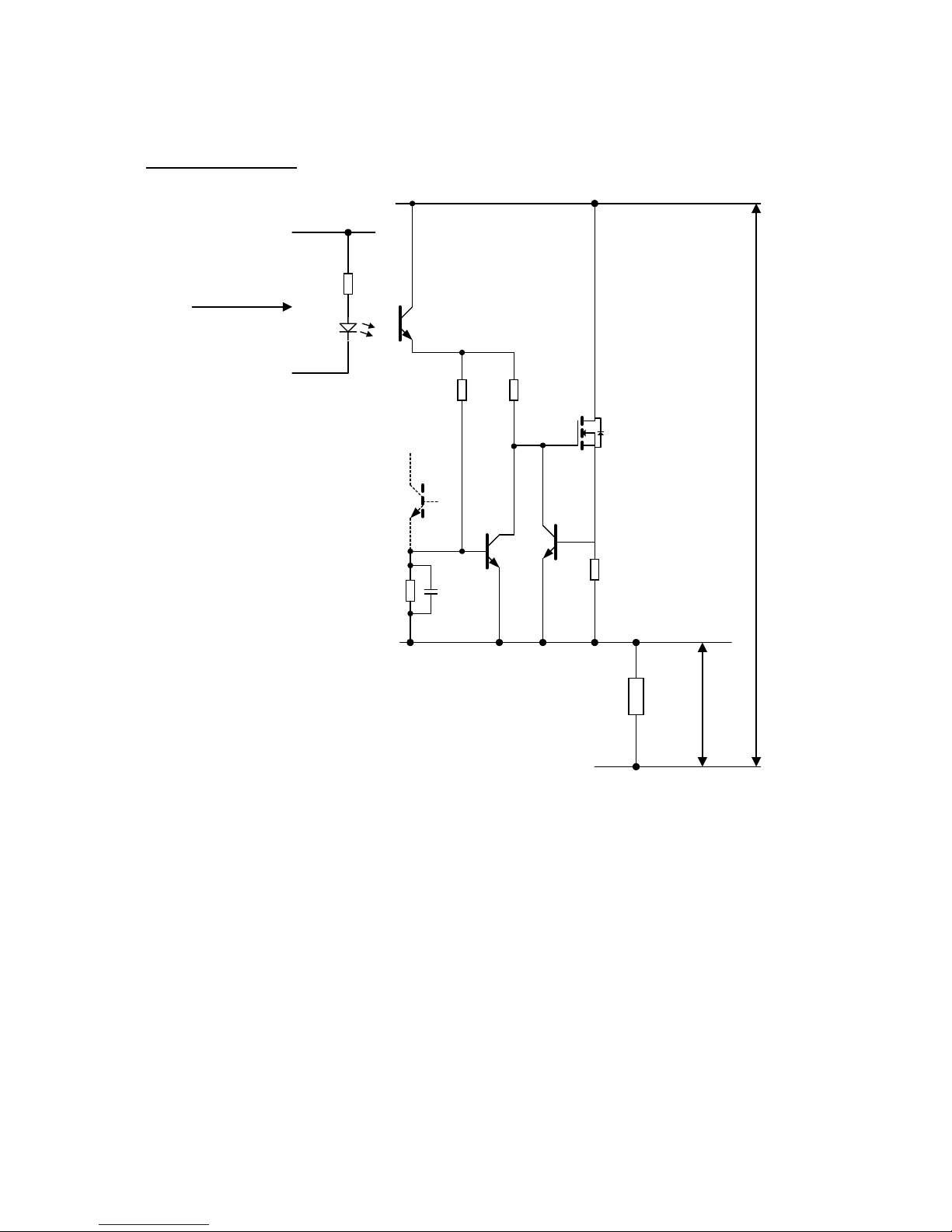
3.5 I/O Interface
3.5.1 Output Circuit
2k2
22k
Supply Voltage
22k
Q1
Q2
Q3
Q4
330R
+3.3V
From Logic
Device
OPTO1
1R8
Output
Voltage
R Load
10nF
Figure 4 Output Circuit
When the opto-is olator is turned on, Q1 will be turned on. The com bination of Q1 and Q2 limits the
current flow through Q1 to about 250mA. If too high a voltage is dropped across Q1 when the output is
on Q4 will turn on, switching off Q1. This limits the maximum dissipation of Q1 to about 1W. If the
output is turned on to a low impedance load the charging of the capacitor delays the turn on of Q4,
allowing for a short surge current to be provided.
The voltage across Q1 incr eases as the load current increases. At 100m A load the voltage drop is
about 2.5V giving a power dissipation of about 250mW per output. At 250mA it is about 3.5V giving a
power dissipation of 900mW. It should be noted that the maximum power dissipation allowed by the
PMC specification is 6W thus limiting the output load that can be used.
Q3 is not used in the output circuit, as it is part of the input c ircuit but is still present on the output
circuit due to commonality of build options.
Note that Figure 4 above shows the output load on the low-voltage side. As the output signals are
voltage-free, the output load may alternatively be connected on the high-voltage side.

PMCCTR32
8
Copyright 2001 BVM Ltd.
3.5.2 Input Circuit
150R
22k
Input Voltage
22k
Q1
Q2
Q3
Q4
1k5
+3.3V
To Logic
Device
OPTO1
10nF
1k
Figure 5 Input Circuit
As the input voltage increases, Q3 turns on which in causes the opto-isolator to be turned on. The
combination of Q3 and Q4 limits the current flow to about 4mA over the full input voltage range.
The input current ranges between 3.5mA f or 12V and 4.5mA for 48V. The power dissipation for an
input is thus 42mW to 220mW depending on the voltage.
Q1 and Q2 are not used in the input circuit, as they are part of the output circ uit but are s till pr esent on
the input circuit due to commonality of build options.
3.6 93CS56 EEPROM
The PMCCTR32 is fitted with a 93CS56 EEPROM which is supplied pre-pr ogrammed by BVM. The
contents of this EEPROM are read by the PCI9030 on coming out of r eset and are us ed to s et up the
control registers after reset, configuring the PCI interface configuration, PCI Device/Vendor ID's &
various other board specific parameters. See section "7.1 PCI Configuration Details ( on page 13) " and
"A.1 PCI9030 PCI Interface (on page 19)" for further details.
3.7 18V256 EEPROM
The PMCCTR32 is fitted with a 18V256 EEPROM, which is supplied pre-programmed by BVM. T he
contents of this EEPROM are read by the SpartanXL FPGA on power up and are used to initialise the
logic functions in the FPGA.

9
PMCCTR32
Copyright 2001 BVM Ltd.
4. Installation
1. PMC modules should only be installed when the host carrier board is in a powered-off c ondition to
avoid damage to the PMC module and host carrier board.
2. After removing any blanking panels on the host c arrier front panel, the PMC module should be
offered up to the host carrier site and the front panel carefully positioned through the host carrier
front panel opening, taking care not to damage the EMC gasket on the PMC module front panel.
3. The PMC module should be fixed to the host carr ier using f our M2.5 x 6m m pan-head s crews into
the four fixing holes provided (two on the front panel and two on the spacers).
4. There is no voltage keying on the PMCCTR32, it will work in both +3.3V and +5V host carriers.
5. The PMCCTR32 can be used with a BVM supplied connecting lead to standard 9-pin D-type
connectors, or a user supplied alternative.
6. The installation can be tested with the example software on the Windows
®
Driver Disc - see
section "7.5 Windows
®
Driver Disc (on page 17)".
5. Configuration
5.1 Link Settings
There are no user configurable links on the PMCCTR32 - each I/O c hannel is selected as an input or
an output at build-time.

PMCCTR32
10
Copyright 2001 BVM Ltd.
6. Connections
6.1 Front Panel Connector
The I/O signals are available through a 68-pin SCSI-III style connector fitted to the f ront of the board the pin-out is shown below. If a PMC I/O board is used the D-type connector pin-out equivalents are
also shown below - see section "6.3 PMC I/O Board (on page 11)" for further details.
Pin No. Signal D-type D-type Signal Pin No.
1 CTOUT0+ P1-1 P5-1 CTGTE0+ 35
2 CTOUT0- P1-6 P5-6 CTGTE0- 36
3 CTOUT1+ P1-2 P5-2 CTGTE1+ 37
4 CTOUT1- P1-7 P5-7 CTGTE1- 38
5 CTOUT2+ P1-3 P5-3 CTGTE2+ 39
6 CTOUT2- P1-8 P5-8 CTGTE2- 40
7 CTOUT3+ P1-4 P5-4 CTGTE3+ 41
8 CTOUT3- P1-9 P5-9 CTGTE3- 42
9 CTOUT4+ P2-1 P6-1 CTGTE4+ 43
10 CTOUT4- P2-6 P6-6 CTGTE4- 44
11 CTOUT5+ P2-2 P6-2 CTGTE5+ 45
12 CTOUT5- P2-7 P6-7 CTGTE5- 46
13 CTOUT6+ P2-3 P6-3 CTGTE6+ 47
14 CTOUT6- P2-8 P6-8 CTGTE6- 48
15 CTOUT7+ P2-4 P6-4 CTGTE7+ 49
16 CTOUT7- P2-9 P6-9 CTGTE7- 50
17 N/C N/C N/C N/C 51
18 N/C N/C N/C N/C 52
19 CTCLK0+ P3-1 P7-1 CTDIR0+ 53
20 CTCLK0- P3-6 P7-6 CTDIR0- 54
21 CTCLK1+ P3-2 P7-2 CTDIR1+ 55
22 CTCLK1- P3-7 P7-7 CTDIR1- 56
23 CTCLK2+ P3-3 P7-3 CTDIR2+ 57
24 CTCLK2- P3-8 P7-8 CTDIR2- 58
25 CTCLK3+ P3-4 P7-4 CTDIR3+ 59
26 CTCLK3- P3-9 P7-9 CTDIR3- 60
27 CTCLK4+ P4-1 P8-1 CTDIR4+ 61
28 CTCLK4- P4-6 P8-6 CTDIR4- 62
29 CTCLK5+ P4-2 P8-2 CTDIR5+ 63
30 CTCLK5- P4-7 P8-7 CTDIR5- 64
31 CTCLK6+ P4-3 P8-3 CTDIR6+ 65
32 CTCLK6- P4-8 P8-8 CTDIR6- 66
33 CTCLK7+ P4-4 P8-4 CTDIR7+ 67
34 CTCLK7- P4-9 P8-9 CTDIR7- 68
Note: CTOUT= Counter/Timer Output
CTCLK = Counter/Timer Clock
CTGTE = Counter/Timer Gate
CTDIR = Counter/Timer Direction

11
PMCCTR32
Copyright 2001 BVM Ltd.
6.2 Rear I/O Connector
The I/O signals are also connected to the P4 connec tor - the pin-out is shown below. This pin-out is
compatible with the BVM cIO200 used with cPC200 i.e. the same lead may be used with the front
panel or rear panel I/O. W ith the rear panel ther e are no com m on pins supplied from the PMCCT R32.
If the rear I/O is to be used it is important that a suitable common is provided.
Pin No. Signal Signal Pin No.
1 CTOUT0+ CTGTE0+ 2
3 CTOUT0- CTGTE0- 4
5 CTOUT1+ CTGTE1+ 6
7 CTOUT1- CTGTE1- 8
9 CTOUT2+ CTGTE2+ 10
11 CTOUT2- CTGTE2- 12
13 CTOUT3+ CTGTE3+ 14
15 CTOUT3- CTGTE3- 16
17 CTOUT4+ CTGTE4+ 18
19 CTOUT4- CTGTE4- 20
21 CTOUT5+ CTGTE5+ 22
23 CTOUT5- CTGTE5- 24
25 CTOUT6+ CTGTE6+ 26
27 CTOUT6- CTGTE6- 28
29 CTOUT7+ CTGTE7+ 30
31 CTOUT7- CTGTE7- 32
33 CTCLK0+ CTDIR0+ 34
35 CTCLK0- CTDIR0- 36
37 CTCLK1+ CTDIR1+ 38
39 CTCLK1- CTDIR1- 40
41 CTCLK2+ CTDIR2+ 42
43 CTCLK2- CTDIR2- 44
45 CTCLK3+ CTDIR3+ 46
47 CTCLK3- CTDIR3- 48
49 CTCLK4+ CTDIR4+ 50
51 CTCLK4- CTDIR4- 52
53 CTCLK5+ CTDIR5+ 54
55 CTCLK5- CTDIR5- 56
57 CTCLK6+ CTDIR6+ 58
59 CTCLK6- CTDIR6- 60
61 CTCLK7+ CTDIR7+ 62
63 CTCLK7- CTDIR7- 64
6.3 PMC I/O Board
If required, a SCSI-III style lead can be used to connect to the BVM 8 Port PMC I/O Board fr om either
the Front Panel Connector or the Rear I/O Connector providing 8 off 9 pin D-type connectors - see
section "1.3 PMC I/O Board Part Number s (on page 1)" - in which c ase the resulting 9 pin D-type pinouts are shown below in Figure 6.
1
2
3
4
5
6
7
8
9
CTXXX0
+
CTXXX1
+
CTXXX2
+
CTXXX3
+
N/C
CTXXX0
-
CTXXX1
-
CTXXX2
-
CTXXX3
-
XXX = OUT/
CLK/GTE/DIR
1
2
3
4
5
6
7
8
9
CTXXX4
+
CTXXX5
+
CTXXX6
+
CTXXX7
+
N/C
CTXXX4
-
CTXXX5
-
CTXXX6
-
CTXXX7
-
XXX = OUT/
CLK/GTE/DIR
Figure 6 Connector Pin-outs for 9-pin D-type

PMCCTR32
12
Copyright 2001 BVM Ltd.
6.4 PCI Connections
P1 and P2 provide the standard PCI signals on the PMC m odule, as def ined in the PMC spec ification
and reproduced for reference purposes below.
P1 32 Bit PCI P2 32 Bit PCI
Pin Signal
Name
Signal
Name
Pin Pin Signal
Name
Signal
Name
Pin
1 TCK -12V 2 1 +12V TRST# 2
3 Ground INTA# 4 3 TMS TDO 4
5 INTB# INTC# 6 5 TDI Ground 6
7 BUSMODE1# +5V 8 7 Ground PCI-RSVD* 8
9 INTD# PCI-RSVD* 10 9 PCI-RSVD* PCI-RSVD* 10
11 Ground PCI-RSVD* 12 11 BUSMODE2# +3.3V 12
13 CLK Ground 14 13 RST# BUSMODE3# 14
15 Ground GNT# 16 15 3.3V BUSMODE4# 16
17 REQ# +5V 18 17 PME# Ground 18
19 V (I/O) AD[31] 20 19 AD[30] AD[29] 20
21 AD[28] AD[27] 22 21 Ground AD[26] 22
23 AD[25] Ground 24 23 AD[24] +3.3V 24
25 Ground C/BE[3]# 26 25 IDSEL AD[23] 26
27 AD[22] AD[21] 28 27 +3.3V AD[20] 28
29 AD[19] +5V 30 29 AD[18] Ground 30
31 V (I/O) AD[17] 32 31 AD[16] C/BE[2]# 32
33 FRAME# Ground 34 33 Ground PMC-RSVD 34
35 Ground IRDY# 36 35 TRDY# +3.3V 36
37 DEVSEL# +5V 38 37 Ground STOP# 38
39 Ground LOCK# 40 39 PERR# Ground 40
41 SDONE# SBO# 42 41 +3.3V SERR# 42
43 PAR Ground 44 43 C/BE[1]# Ground 44
45 V (I/O) AD[15] 46 45 AD[14] AD[13] 46
47 AD[12] AD[11] 48 47 Ground AD[10] 48
49 AD[09] +5V 50 49 AD[08] +3.3V 50
51 Ground C/BE[0]# 52 51 AD[07] PMC-RSVD 52
53 AD[06] AD[05] 54 53 +3.3V PMC-RSVD 54
55 AD[04] Ground 56 55 PMC-RSVD Ground 56
57 V (I/O) AD[03] 58 57 PMC-RSVD PMC-RSVD 58
59 AD[02] AD[01] 60 59 Ground PMC-RSVD 60
61 AD[00] +5V 62 61 ACK64# +3.3V 62
63 Ground REQ64# 64 63 Ground PMC-RSVD 64

13
PMCCTR32
Copyright 2001 BVM Ltd.
7. Programming
7.1 PCI Configuration Details
A pre-programm ed EEPROM contains the BVM PCI Vendor ID, which is 15C0 (hexadecim al) and the
PCI Device ID, which is 02FF (hexadecim al) and the BVM PCI Subsystem Vendor ID, which is 15C0
(hexadecimal) and the PCI Subsystem Device ID, which is 020C (hexadecimal).
7.2 Address Map
The PMCCTR32 uses BAR2 for access to the user accessible registers which are m apped into PCI
memory space as shown below. BAR0 is used for access to the PCI9030 configuration r egister of f s ets
which are also mapped into PCI memory space. Details of PCI9030 conf iguration are not covered in
this User's Manual - see section "A.1 PCI9030 PCI Interface (on page 19)" for fur ther details. BAR1,
BAR3 and above are unused.
Address Description Access Size
000 Counter/Timer Output Register R 8
001 Counter/Timer Clock Register R 8
002 Counter/Timer Gate Register R 8
003 Counter/Timer Direction Register R 8
009 - 004 Reserved (reads 0) R
00A Counter/Timer Gate Override Register R/W 8
00B Counter/Timer Dir. Override Register R/W 8
00F - 00C Reserved (reads 0) R
010 Counter/Timer Status Register R/W 8
011 Counter/Timer Output Control Register R/W 8
012 Counter/Timer Interrupt Enable Register R/W 8
013 Counter/Timer Clock Source Register R/W 8
017 - 014 Reserved (reads 0) R
018 Direction Register R 8
019 Function Register R 8
01B - 01A Status & Control Register R/W 16
0FF - 01C Reserved (reads 0) R
100 Watchdog Trigger Register R/W 8
103 - 101 Unused (undefined)
104 Watchdog Timer Register R/W 8
107 - 105 Unused (undefined)
108 Watchdog Status Register R 8
1FF - 109 Unused (undefined)
201 - 200 Counter/Timer 0 Value Register R/W 16
203 - 202 Reserved (reads 0) R 16
205 - 204 Counter/Timer 1 Value Register R/W 16
207 - 206 Reserved (reads 0) R 16
209 - 208 Counter/Timer 2 Value Register R/W 16
20B - 20A Reserved (reads 0) R 16
20D - 20C Counter/Timer 3 Value Register R/W 16
20F - 20E Reserved (reads 0) R 16
211 - 210 Counter/Timer 4 Value Register R/W 16
213 - 212 Reserved (reads 0) R 16
215 - 214 Counter/Timer 5 Value Register R/W 16
217 - 216 Reserved (reads 0) R 16
219 - 218 Counter/Timer 6 Value Register R/W 16
21B - 21A Reserved (reads 0) R 16
21D - 21C Counter/Timer 7 Value Register R/W 16
21F - 21E Reserved (reads 0) R 16

PMCCTR32
14
Copyright 2001 BVM Ltd.
7.3 Register Descriptions
7.3.1 Counter/Timer Output Register
The 8-bit read only Counter/Timer Output Regis ter contains the levels of the Counter/T imer Output
pins on the logic device. W hen reading back the output signals, no ac count is tak en of values beyond
the I/O buffers. The Counter/Timer Output pins go active when the count crosses the 0000/FFFF
boundary - active LOW or HIGH is selected in the Counter/Timer Output Control Register - see
section "7.3.8 Counter/Timer Output Control Register (below)".
7.3.2 Counter/Timer Clock Register
The 8-bit read only Counter/Timer Clock Regist er contains the levels of the Counter /Timer Clock pins
on the logic device. W hen reading back the output signals, no ac count is tak en of values beyond the
I/O buffers. The Counter/Timer Clock pins are used to clock the Counter/Timer when the external
clock is selected in the Counter/Timer Clock Source Register - see section "7.3.10 Counter/Timer
Clock Source Register (on page 15)".
7.3.3 Counter/Timer Gate Register
The 8-bit read only Counter/Timer Gate Regis ter contains the levels of the Counter/Tim er Gate pins
on the logic device. W hen reading back the output signals, no ac count is tak en of values beyond the
I/O buffers. The Counter/Timer Gate pins are used to enable the count: HIGH to enable; LOW to
disable. If the Counter/Timer G ate pins are not connected they default to LOW (disabled) and m ay be
overridden - see section "7.3.5 Counter/Timer Gate Override Register (below)".
7.3.4 Counter/Timer Direction Register
The 8-bit read only Counter/Timer Direction Register contains the levels of the Counter/Timer
Direction pins on the logic device. When reading back the output signals, no account is taken of
values beyond the I/O buffers. The Counter/Timer Direction pins are used to control the count
direction: HIGH for UP; LOW for DOW N. If the Counter/Tim er Direction pins are not connected they
default to LOW (count down) and may be overridden - see section "7.3.6 Counter/Timer Direction
Override Register (below)".
7.3.5 Counter/Timer Gate Override Register
The 8-bit read/write Counter/Timer Gate Override Register where each bit corresponds to an individual
Counter/Timer (0 to 7). The bit is OR'ed with the corresponding gate input pin for the respective
Counter/Timer. If the gate input pin is left disconnected then it is a 0, therefore writing a 1 to the
corresponding bit in the Counter/Timer Gate Override Register will enable the Counter/Timer and
writing a 0 will disable the Counter/Timer.
7.3.6 Counter/Timer Direction Override Register
The 8-bit read/write Counter/Timer Direction Override Register where each bit corresponds to an
individual Counter/Timer (0 to 7). T he bit is OR'ed with the corresponding direction input pin for the
respective Counter/Tim er. If the dir ec tion input pin is lef t dis connec ted then it is a 0, ther ef ore writing a
1 to the corresponding bit in the Counter/Timer Gate Override Register will cause the Counter/Timer to
count UP and writing a 0 will cause the Counter/Timer to count DOWN.
7.3.7 Counter/Timer Status Register
The 8-bit read/write Counter/Timer Status Register where each bit corresponds to an individual
Counter/Timer (0 to 7). If the corresponding bit is set to 1 then the relevant Counter/Timer output is
active - writing a 1 to the corresponding bit clears this state and clears the interrupt.
7.3.8 Counter/Timer Output Control Register
The 8-bit write only Counter/Timer Output Control Register where each bit corresponds to an
individual Counter/Timer (0 to 7). If the corresponding bit is set to 1 then the relevant Counter/T imer
output is active HIGH otherwise the output is active LOW.
7.3.9 Counter/Timer Interrupt Enable Register
The 8-bit read/write Counter/Timer Interrupt Enable Register where each bit corresponds to an
individual Counter/Timer (0 to 7). If the corresponding bit is set to 1 then the relevant Counter/T imer
interrupt is enabled and an interrupt will be generated when the output is active. The interrupt may be
cleared by writing a 1 to the relevant bit in the Counter/Timer Interrupt Enable Register or by clearing
the output - see section"7.3.7 Counter/Timer Status Register (above)".

15
PMCCTR32
Copyright 2001 BVM Ltd.
7.3.10 Counter/Timer Clock Source Register
The 8-bit write only Counter/Timer Clock Source Register where each bit corres ponds to an individual
Counter/Timer (0 to 7). If the corresponding bit is set to 1 then the r elevant Counter/Tim er clock input
is driven from the internal clock otherwise the clock input is driven from the external clock - see
section "7.3.2 Counter/Timer Clock Register (on page 14)".
7.3.11 Direction Register
The 8-bit read only Direction Register where each of the leas t significant four bits correspond to a
group of 8 I/O bits. If the corres ponding bit is set to 1 the bit is an output otherwise it is an input.
Reserved bits (RSVD) read as zero.
7 6 5 4 3 2 1 0
RSVD RSVD RSVD RSVD 0 0 0 1
7.3.12 Function Register
The 8-bit read only Function Register contains the low byte of the PCI Subsystem Device ID - see
section "7.1 PCI Configuration Details (on page 13)". This can be us ed to determ ine the type of board
fitted from the PMCDIO and PMCCTR range.
7.3.13 Status & Control Register
The 16-bit read/write Status & Control Register is us ed to c ontrol a number of the module functions as
described below. Reserved bits (RSVD) read as zero and should be written as zero for future
compatibility.
7 6 5 4 3 2 1 0
WDGST IWDEN RSVD GOPEN WINEN RSVD RSVD RSVD
15 14 13 12 11 10 9 8
RSVD RSVD RSVD RSVD RSVD INCLK2 INCLK1 INCLK0
7.3.13.1 Watchdog Interrupt Enable (Bit 3: WINEN)
When set to 1 this bit enables the generation of a PCI Interrupt if an enabled internal watchdog times
out - see section "7.3.13.3 Internal Watchdog Enable (Bit 6: IWDEN) (below)". If c lear no PCI Inter rupt
will be generated.
7.3.13.2 Global Output Enable (Bit 4: GOPEN)
When set to 1 this bit enables all output signals. If clear all output signals ar e disabled. Input signals
are unaffected.
7.3.13.3 Internal Watchdog Enable (Bit 6: IWDEN)
When set to 1 the internal watchdog function is enabled and if the watchdog times-out then the
outputs will be disabled. If clear the state of the watchdog is ignored.
7.3.13.4 Watchdog Status (Bit 7: WDGST)
When set to 1 this bit indicates an enabled inter nal watchdog has timed-out - see section "7.3.13.3
Internal Watchdog Enable (Bit 6: IWDEN) (above)". Once set this bit cannot be cleared.

PMCCTR32
16
Copyright 2001 BVM Ltd.
7.3.13.5 Internal Counter/Timer Clock/De-bounce (Bit 10..8: INCLK2..0)
These bits set the clock frequency for the Counter/Timers when select ed as internally clocked - see
section "7.3.10 Counter/Timer Clock Source Register (on page 15)". These bits also set the debounce period as shown below when clocked internally or externally.
INCLK0-2 Clock Frequency De-bounce Period
0 260kHz
2µS
1 130kHz
4µS
2 65kHz
8µS
3 32kHz
15µS
4 16kHz
31µS
5 8kHz
61µS
6 4kHz
120µS
7 2kHz
250µS
7.3.14 Watchdog Trigger Register
The 8-bit read/write W atchdog Trigger Register mus t be written to with bit 0 set to 0 and 1 alternately
within ±25% of the watchdog refresh time when the watchdog function is enabled in the Status &
Control Register - see section "7.3.13 Status & Control Register (on page 15)".
7.3.15 Watchdog Timer Register
The 8-bit read/write Watchdog Tim er Register is used to set the refresh period. The watchdog tim er
runs from its own independent 32.768kHz oscillator and has a program mable refr esh period between
125ms and 2sec. On reset the watchdog is not running and has a refresh period of 125ms. The
watchdog timer is started by the first write to the watchdog trigger register. Bits 2 - 0 set the refresh
period, bits 7 - 3 are undefined on a read and should be written as zero for future compatibility.
Note that once the internal watchdog is running, this register is read only - writing to the regist er will
cause the watchdog to trigger.
Bits
2 - 0
Watchdog Refresh Period
0 125ms
1 250ms
2 500ms
3 1.0sec
4 2.0sec
5 2.0sec
6 2.0sec
7 2.0sec

17
PMCCTR32
Copyright 2001 BVM Ltd.
7.3.16 Watchdog Status Register
The 8-bit read only Watchdog Status Register is us ed to determine the st atus of the watchdog. When
bit 0 is read as 1 the watchdog function is enabled, when bit 1 is read as 1 the watchdog f unction has
been started, bits 7 - 2 are undefined when read.
Note that writing to this register whilst the internal watchdog is running will cause the watchdog to
trigger.
Bits
1 - 0
Watchdog Status
0 Not Started
1 Illegal State
2 Tripped
3 Running
7.4 Interrupts
PCI INTA# is generated when a Counter/Timer Output goes active after being enabled or a watchdog
time-out occurs af ter the watchdog is enabled. The interr upt will be removed when the Counter/T imer
Output is cleared and when the Counter/Timer interrupt is disabled - see section "7.3.9 Counter /Tim er
Interrupt Enable Register (on page 14)" and when the watchdog interrupt is disabled - see section
"7.3.13.1 Watchdog Interrupt Enable (Bit 3: WINEN) (on page 15)".
7.5 Windows® Driver Disc
BVM can supply a disc containing the driver files and example source code for W indows® 98, NT4.0
and 2000 along with BVM installation files. The BVM installation files will ens ure that the corr ect driver
configuration is selected upon installation.

PMCCTR32
18
Copyright 2001 BVM Ltd.
8. Specification
8.1 On-Board Functions
8.1.1 PCI9030 PCI Interface
PCI 2.2 compliant 32-bit, 33-MHz Bus Target Interface Device
PCI Target Read Ahead mode disabled
PCI Target Delayed Read mode disabled
PCI Target Delayed Write mode disabled
Programmable Interrupt Generator
Local Bus provides 32-bit non-multiplexed 16-bit peripheral access
Local Bus zero wait state
Programmable Local-to-PCI interrupt
8.1.2 SpartanXL FPGA
Counter/Timer Output Register
Counter/Timer Clock Register
Counter/Timer Gate Register
Counter/Timer Direction Register
Counter/Timer Status Register
Counter/Timer Output Control Register
Counter/Timer Interrupt Enable Register
Counter/Timer Clock Source Register
Direction Register
Function Register
Status & Control Register
Watchdog Trigger Register
Watchdog Timer Register
Watchdog Status Register
8 x Counter/Timer Value Registers
8.1.3 Local Clocks
32.768KHz timer clock
8.2 Board Configuration
EEPROM: PCI Configuration, FPGA Configuration
8.3 I/O Interface
32-bits of opto-isolated I/O
I/O direction fixed
Global output enable
2kV I/O to logic isolation
1kV I/O to I/O isolation
5mA input current limit
250mA output current limit
Short-circuit protection
8.4 Counter/Timer Functions
8 x 16-bit Counter/Timers
External or Internal Clock Input
Internal Clock Frequency Select
External Gate Input
External Direction Input
External Output on Count Rollover
Interrupt on Count Rollover

19
PMCCTR32
Copyright 2001 BVM Ltd.
8.5 PMC Interface
Bus Interface: PCI 2.2 compliant
Bus Width: 32-bit
Bus Speed: 33MHz
Data Transfer: PCI 2.2 Bus Target
Interrupts: PCI INT #A
Memory Address: BIOS assigned
8.6 Operating Environment
Dimensions: 74.0mm x 149.0mm (single PMC size)
Power: +3.3V 215mA typical
+5V 0mA, excluding external requirements
Environmental: 0 to 70 °C, 95%
humidity non-condensing (extended range to order)
Appendix A - Data Sheets & Manual References
A.1 PCI9030 PCI Interface
PLX PCI9030 PCI SMARTarget™ I/O Accelerator, Data Book Version 1.0 April 2000.
(http://www.plxtech.com)
A.2 Spartan-XL FPGA
Spartan and SpartanXL Families Field Programmable Gate Arrays DS060 (V1.5) March 2, 2000.
(http://www.xilinx.com)
A.3 Si4946EY Dual N-Channel MOSFET
Vishay Siliconix Si4946EY Dual N-Channel 60-V (D-S) 175°C MOSFET, Document Num ber : 70157 S57253—Rev. C, 24-Feb-98.
(http://www.vishay.com)
A.4 SST2222A NPN Transistor
Rohm UMT2222A / SST2222A / MMST2222A PN2222A NPN Medium Power Transistor (Switching),
Data Sheet.
(http://www.vishay.com)
A.5 K817P Four Channel Opto-isolator
Vishay Telefunken K817P/ K827PH/ K847PH Optocoupler with Phototransistor O utput, Data Sheet:
Rev. A2, 11–Jan–99.
(http://www.vishay.com)
A.6 PMC Specification
IEEE Draft Standard Physical and Environmental Layers for PCI Mezzanine Cards: PMC
P1386.1/Draft 2.3 9
th
October 2000.
(http://www.ieee.org)
 Loading...