

Page 1

Artisan Technology Group is your source for quality
new and certied-used/pre-owned equipment
• FAST SHIPPING AND
DELIVERY
• TENS OF THOUSANDS OF
IN-STOCK ITEMS
• EQUIPMENT DEMOS
• HUNDREDS OF
MANUFACTURERS
SUPPORTED
• LEASING/MONTHLY
RENTALS
• ITAR CERTIFIED
SECURE ASSET SOLUTIONS
SERVICE CENTER REPAIRS
Experienced engineers and technicians on staff
at our full-service, in-house repair center
Instra
Remotely inspect equipment before purchasing with
our interactive website at www.instraview.com
Contact us: (888) 88-SOURCE | [email protected] | www.artisantg.com
SM
REMOTE INSPECTION
View
WE BUY USED EQUIPMENT
Sell your excess, underutilized, and idle used equipment
We also offer credit for buy-backs and trade-ins
www.artisantg.com/WeBuyEquipment
LOOKING FOR MORE INFORMATION?
Visit us on the web at www.artisantg.com for more
information on price quotations, drivers, technical
specications, manuals, and documentation
Page 2

PRELIMINARY
ProDAQ 3150
High-Perfomance Motherboard
User Manual
Bustec Production Ltd.
World Aviation Park
Shannon, Co. Clare, Ireland
Tel. +353 61 707 100
Fax +353 61 707 106
www.bustec.ie
Publication No. 3150UM-01
Publication Date: Oct. 2000
Copyright, 2000, Bustec Production Ltd.
PROPRIETARY NOTICE
This document and the technical data herein disclosed, are proprietary to Bustec Production Ltd.,
and shall not, without express written permission of Bustec Production Ltd., be used, in whole or in
part to solicit quotations from a competitive source or used for manufacture by anyone other than
Bustec Production Ltd. The information herein has been developed at private expense, and may
only be used for operation and maintenance reference purposes or for purposes of engineering
evaluation and incorporation into technical specifications and other documents, which specify
procurement of products from Bustec Production Ltd. This is a preliminary document and can be
subject to change without further notification. Bustec Production Ltd. reserve the right to change
both the hardware and software prototypes described herein.
Artisan Technology Group - Quality Instrumentation ... Guaranteed | (888) 88-SOURCE | www.artisantg.com
Page 3

WARRANTY STATEMENT
Products sold by Bustec Production Ltd. are warranted to be free from defects in workmanship or
materials. Bustec Production Ltd. at its discretion will either repair or replace any hardware
products that prove to be defective during the warranty period. You are a valued customer. Our
mission is to make any necessary repairs in a reliable and timely manner.
Duration of Warranty
The warranty period for Bustec Production Ltd. hardware is one year. Software and firmware
products designed for use with this hardware are warranted not to fail to execute their
programming instructions due to defect in materials or workmanship for a period of ninety days
from the date of delivery to the initial end user.
Return of Product
Authorization is required from Bustec Production Ltd. before you send us your product for service
or calibration. Call Bustec Production Ltd support facility. If you are unsure where to call, contact
Bustec Production Ltd. at 353-61-707100. We can also be reached at www.bustec.ie.
Limitation of Warranty
Bustec Production Ltd. shall be released from all obligations under this warranty in the event
repairs or modifications are made by persons other than authorized Bustec Production Ltd. service
personnel or without the written consent of Bustec Production Ltd.
Bustec Production Ltd. expressly disclaims any liability to its customers, dealers and
representatives and to users of its product. Also to any other person or persons, for special or
consequential damages of any kind and from any cause whatsoever arising out of or in any way
connected with the manufacture, sale, handling, repair, maintenance, replacement or use of said
products.
Representations and warranties made by any person including dealers and representatives of
Bustec Production Ltd., which are inconsistent or in conflict with the terms of this warranty
(including but not limited to the limitations of the liability of Bustec Production Ltd. as set forth
above), shall not be binding upon Bustec Production Ltd. unless reduced to writing and approved
by an officer of Bustec Production Ltd.
Except as stated above, Bustec Production Ltd. makes no warranty, express or implied (either in
fact or by operation of law), statutory or otherwise; and except to the extent stated above. Bustec
Production Ltd. shall have no liability under any warranty, express or implied (either in fact or by
operation of law), statutory or otherwise.
Artisan Technology Group - Quality Instrumentation ... Guaranteed | (888) 88-SOURCE | www.artisantg.com
Page 4

Table of Contents
1 Introduction ............................................................................................................................................. 5
1.1 About the ProDAQ 3150 Motherboard .............................................................................................. 5
1.2 Unpacking and Inspection ................................................................................................................. 6
1.3 Reshipment Instructions .................................................................................................................... 7
2 Installation and Configuration ................................................................................................................ 8
2.1 Installing a ProDAQ Function Card ................................................................................................... 9
2.2 Removing a ProDAQ Function Card ............................................................................................... 11
2.3 Installing a ProDAQ Plug-in Module ................................................................................................ 11
2.3.1 Installing the ProDAQ Voltage Reference Plug-in Module ....................................................... 12
2.3.2 Installing the ProDAQ DSP Plug-in Module ............................................................................. 12
2.4 Configuring the ProDAQ 3150 Motherboard ................................................................................... 13
2.4.1 VXIbus Logical Address ........................................................................................................... 13
3 Theory of Operation .............................................................................................................................. 15
3.1 Overview .......................................................................................................................................... 16
3.2 VXIbus Interface .............................................................................................................................. 16
3.2.1 VXIbus Configuration Registers ................................................................................................ 16
3.2.2 Interrupter ................................................................................................................................. 16
3.3 Memory ............................................................................................................................................ 17
3.4 On-board processor ......................................................................................................................... 17
3.5 Communication/Arbitration Controller ............................................................................................... 17
3.6 The Trigger and Interrupt System ..................................................................................................... 18
4 Programming Information .................................................................................................................... 20
4.1 VXIbus Interface and Registers........................................................................................................ 20
4.1.1 VXIbus Configuration Registers ............................................................................................... 21
4.1.2 VXIbus Configuration Register Details ..................................................................................... 22
4.2 VXIbus Address Map ....................................................................................................................... 35
4.2.1 Function Card Access .............................................................................................................. 36
4.2.2 Internal Resource ..................................................................................................................... 37
5 The ProDAQ 3220 DSP Plug-in Module .............................................................................................. 39
5.1 Overview........................................................................................................................................... 39
5.2 Programming Information ................................................................................................................ 40
5.2.1 Address Map ............................................................................................................................ 40
5.2.1 Communication Registers ........................................................................................................ 41
5.3 iBus Cycles....................................................................................................................................... 49
5.4 VXI Local Bus Interface .................................................................................................................... 51
Artisan Technology Group - Quality Instrumentation ... Guaranteed | (888) 88-SOURCE | www.artisantg.com
Page 5

List of Figures
Figure 1 - Components of a ProDAQ Modular Data Aquisition System ............................................................ 6
Figure 2 - Removing the ProDAQ Module Cover ............................................................................................. 8
Figure 3 - The module assembly ................................................................................................................... 10
Figure 4 - Location of Plug-in Modules and Memory ..................................................................................... 11
Figure 5 - Logical Address Selection ............................................................................................................. 13
Figure 6 - Simplified Block Diagram ............................................................................................................... 15
Figure 7 - DSP Plug-in Module Block Diagram .............................................................................................. 39
Artisan Technology Group - Quality Instrumentation ... Guaranteed | (888) 88-SOURCE | www.artisantg.com
Page 6

ProDAQ 3150 User Manual 3150UM-01
Chapter 1
Introduction
This manual describes the ProDAQ 3150 Motherboard and explains how to install, configure and program
the ProDAQ 3150 Motherboard with any of the ProDAQ Plug-in Modules and ProDAQ Function Cards.
About the ProDAQ 3150 Motherboard
The ProDAQ 3150 Motherboard provides a VXI interface, a local processor, memory and common resources
like a voltage reference module (optional), trigger routing capability and additional power regulators for up to
eight ProDAQ function cards. The ProDAQ 3150 Motherboard together with the ProDAQ Function Cards can
be configured to provide any function or combination of functions required for a specific application.
The ProDAQ 3150 Motherboard is part of the ProDAQ Modular Data Acquisition System, which consists of
the following components:
A ProDAQ Motherboard that installs into a VXI slot in a VXIbus chassis. A ProDAQ Motherboard can
be populated with a ProDAQ 3250 DSP Plug-in Module (ProDAQ 3150 Motherboard only), a
ProDAQ 3201 Voltage Reference Plug-in Module (optional) and up to eight ProDAQ Function Cards.
The ProDAQ 3220 DSP Plug-in Module that installs into the DSP Plug-in slot on a ProDAQ
Motherboard (ProDAQ 3150 Motherboard only).
The ProDAQ 3201 Voltage Reference Plug-in Module that installs into the Voltage Reference Plug-in
slot on a ProDAQ Motherboard.
The ProDAQ Function Cards which install into ProDAQ Bus slots on a ProDAQ Motherboard.
The ProDAQ Signal Conditioning Unit can be used together with the ProDAQ Modular Data Acquisition
System to provide various signal conditioning functions and allows for easy connection to the existing
installation.
Bustec Production Ltd. Page 5
Artisan Technology Group - Quality Instrumentation ... Guaranteed | (888) 88-SOURCE | www.artisantg.com
Page 7
ProDAQ 3150 User Manual 3150UM-01
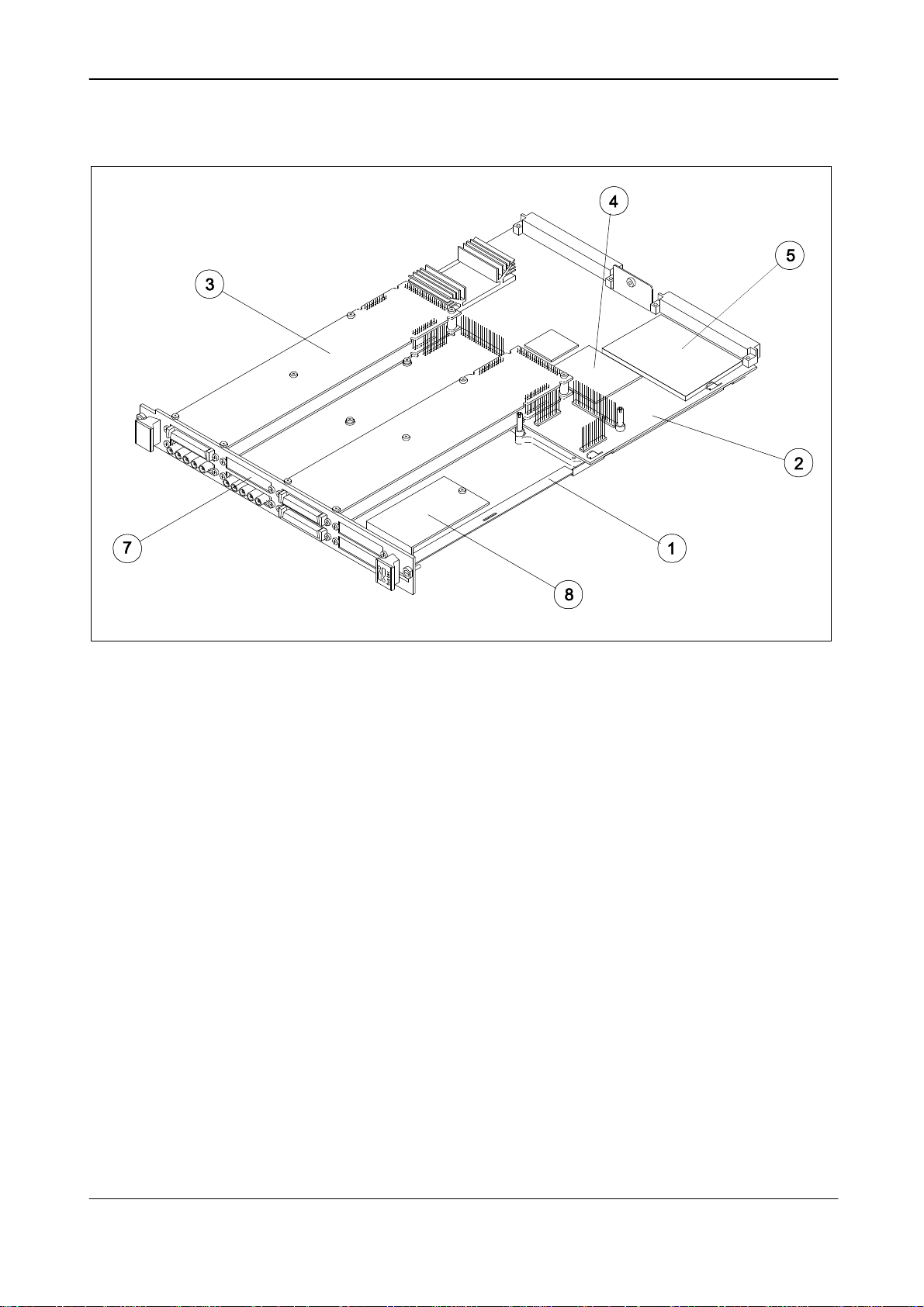
1 - Module Cover (Bottom) 2 - ProDAQ Motherboard 3 - ProDAQ Function Card
4 - ProDAQ Voltage Ref. Plug-in Module 5 - ProDAQ DSP Plug-in Module 6 - Memory Plug-in Module
7 - Single Filler Panel 8 - Double Filler Panel
Figure 1 - Components of a ProDAQ Modular Data Aquisition System
The ProDAQ 3150 Motherboard is shipped in a VXI module enclosure, ready to be installed in a VXIbus
chassis. The function cards can be factory-installed or field-installed later on. The front-panel is populated
with filler panels for each ProDAQ function card slot, which should be left in place unless a ProDAQ function
card is installed in the slot. The ProDAQ function card slots are arranged in four stacks of two function cards
each.
Unpacking and Inspection
Before unpacking the ProDAQ module, check the exterior of the shipping carton for any signs of damage. All
irregularities should be noted on the shipping bill.
The ProDAQ module is shipped in an antistatic package to prevent any damage from electrostatic discharge
(ESD). Proper ESD handling procedures must always be used when packing, unpacking or installing any
ProDAQ module, ProDAQ plug-in module or ProDAQ function card:
Ground yourself via a grounding strap or similar, e.g. by holding to a grounded object.
Page 6 Bustec Production Ltd.
Artisan Technology Group - Quality Instrumentation ... Guaranteed | (888) 88-SOURCE | www.artisantg.com
Page 8

ProDAQ 3150 User Manual 3150UM-01
Discharge the package by touching it to a grounded object, e.g. a metal part of your VXIbus chassis,
before removing the module from the package.
Remove the ProDAQ module from its carton, preserving the factory packaging as much as possible.
Inspect the ProDAQ module for any defect or damage. Immediately notify the carrier if any damage
is apparent.
Reshipment Instructions
Use the original packing material when returning a ProDAQ module to Bustec Production Ltd. or calibration
or servicing. The original shipping carton and the instrument's plastic foam will provide the necessary support
for safe reshipment.
If the original anti-static packing material is unavailable, wrap the ProDAQ module in anti-static plastic
sheeting and use plastic spray foam to surround and protect the instrument. Reship in either the original or a
new shipping carton.
Bustec Production Ltd. Page 7
Artisan Technology Group - Quality Instrumentation ... Guaranteed | (888) 88-SOURCE | www.artisantg.com
Page 9
ProDAQ 3150 User Manual 3150UM-01
Chapter 2
Installation and Configuration
To install a ProDAQ Plug-in Module or a ProDAQ Function Card as well as to configure the addressing mode
of the ProDAQ 3120 Motherboard, you need to remove the modules top cover.
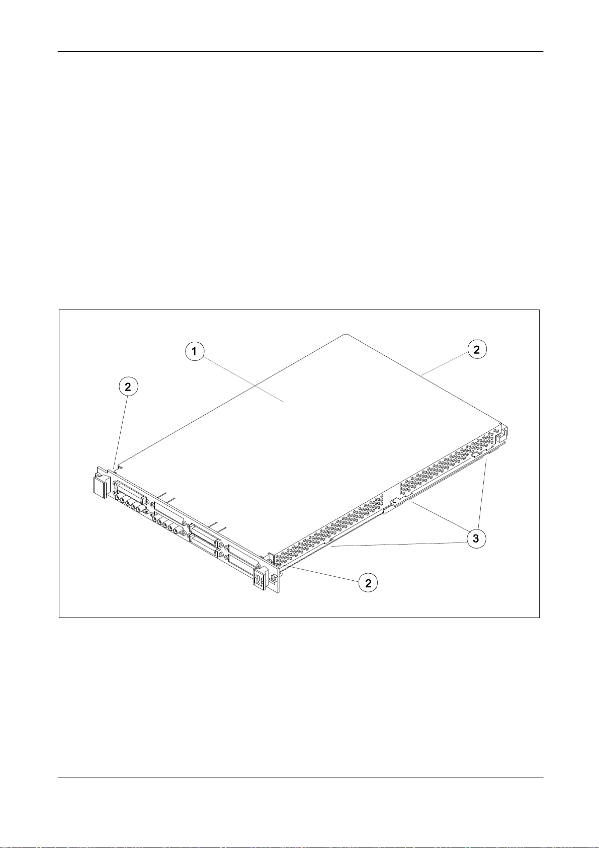
1 - Module Cover 2 - Cover Screws 3 - Cover Hooks
Figure 2 - Removing the ProDAQ Module Cover
To remove the top cover, remove the undercut flathead and two panhead screws that hold the cover in place
and remove the cover by sliding it out of its position towards the VXIbus connectors and up. Take special
care about the hooks holding it into place. Try not to lift the cover straight up. See figure 2 for the location of
the screws.
Page 8 Bustec Production Ltd.
Artisan Technology Group - Quality Instrumentation ... Guaranteed | (888) 88-SOURCE | www.artisantg.com
Page 10

ProDAQ 3150 User Manual 3150UM-01
To re-install the cover, slide it back into its position by placing the small hooks over their holes and moving
the cover down and forward. Secure the top cover using the three undercut flathead screws.
Installing a ProDAQ Function Card
The ProDAQ Function Cards are arranged inside the ProDAQ Module in four stacks of two cards each. The
function cards are mounted face down, e.g. the front-panel connectors as well as the motherboard
connectors are underneath the PCB.
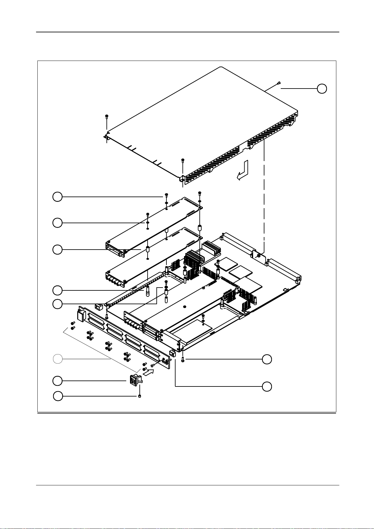
To install a ProDAQ Function Card in any of the possible positions, use the following procedure (See figure 3
for reference):
Remove the top cover of the module as described earlier in this chapter (Fig. 3, Pos. 1).
Remove all screws on the front-panel holding installed function cards or double filler panels in place
(Fig. 3, Pos. 2). Screws holding single filler panels don't need to be removed.
Remove the two panhead screws that mount the front panel to the modules bottom cover (Fig. 3,
Pos. 6).
Please take special care of the module handles and the rings (Fig. 3, Pos. 3 and 4), which are also
fixed by those screws. The mounting angle (Fig. 3, Pos. 5) stays fixed to the front panel.
Remove the front panel by moving it forward carefully so as to avoid bending the installed function
cards.
Choose the stack and position (lower or upper) where you want to mount the function card. If the
stack, in which the function card should be installed, is covered by a double filler panel, you have to
remove it before installing the function card.
Remove the three 2.5mm panhead screws and the crinkle washers from the stack's standoffs (Fig.
3, Pos. 9 and 10 for example).
If you want to install a function card in the upper position of a stack without having a function card in
the lower position, you need to mount both spacers (Fig. 3, Pos. 11) on each standoff. If the stack is
already populated with a function card in the lower position, mount only the bigger spacer (Fig. 3,
Pos. 8) onto each standoff.
Place a bayonet (supplied) on each standoff. Align the function card over these and slide carefully
down. The function card should be held parallel to the modules bottom cover all the time during its
way down.
Fix the function card by mounting the three 2.5mm panhead screws and the crinkle washers onto
each standoff. If you install a function card in the lower position of a stack, you need first to mount
both spacers (Fig. 3, Pos. 11) onto each standoff.
Re-mount the modules front-panel. If there is only one function card mounted in a stack, cover the
remaining opening in the front panel by a single filler panel.
Re-mount the modules top cover.
Bustec Production Ltd. Page 9
Artisan Technology Group - Quality Instrumentation ... Guaranteed | (888) 88-SOURCE | www.artisantg.com
Page 11
ProDAQ 3150 User Manual 3150UM-01
1
10
11
9
8
7
2
3
4
6
5
1 - 2.5mm Panhead Screws 2 - 2.5mm Panhead Screws 3 - Module Handle
4 - Ring 5 - Mounting Angle 6 - 2.5mm Panhead Screws
7 - Standoff 8 - Spacer 9 - Crinkle Washer
10 - 2.5mm Panhead Screw 11 - 2mm Spacer
Figure 3 - The module assembly
Page 10 Bustec Production Ltd.
Artisan Technology Group - Quality Instrumentation ... Guaranteed | (888) 88-SOURCE | www.artisantg.com
Page 12

ProDAQ 3150 User Manual 3150UM-01
Removing a ProDAQ Function Card
Removing a ProDAQ Function Card is exactly the the reverse operation then installing it. After removing the
top cover and the front panel as described previously, remove the three roundhead screws that fix the
function card(s) on the standoffs.
Take special care when removing the function card(s) not to bend the motherboard connectors.
After removing the function card(s), install the correct combination of spacers on the standoffs. If a stack is
populated with only one function card, each of the standoffs needs to be mounted with both spacers to cover
the distance between the cards as well as the PCB thickness of the missing card. If a stack is populated with
two function cards, only the bigger spacer must be mounted.
Fix any remaining function card again by mounting the three panhead screws on the standoffs, re-mount the
front panel and the modules cover.
Installing a ProDAQ Plug-in Module
The ProDAQ 3150 Motherboard Module allows the installation of a Voltage Reference Plug-in Module for
calibration purposes, a ProDAQ 3250 DSP Plug-in Module and memory modules.
Figure 4 - Location of Plug-in Modules and Memory
Bustec Production Ltd. Page 11
Artisan Technology Group - Quality Instrumentation ... Guaranteed | (888) 88-SOURCE | www.artisantg.com
Page 13

ProDAQ 3150 User Manual 3150UM-01
Installing the ProDAQ Voltage Reference Plug-in Module
To install the ProDAQ Voltage Reference Plug-in Module, the top cover of the module has to be removed as
described earlier in this chapter. Locate the position of the plug-in module slot (See Figure 4 for reference).
It features two connectors that need to be aligned and inserted into the motherboard sockets. The
VXIplug&play drivers supplied with the module will automatically detect and configure an installed Voltage
Reference Plug-in Module.
Installing the ProDAQ DSP Plug-in Module
To install the ProDAQ DSP Plug-in Module, the top top cover of the module has to be removed as described
earlier in this chapter. Locate the position of the plug-in module slot (See Figure 4 for reference).
Page 12 Bustec Production Ltd.
Artisan Technology Group - Quality Instrumentation ... Guaranteed | (888) 88-SOURCE | www.artisantg.com
Page 14
ProDAQ 3150 User Manual 3150UM-01
Configuring the ProDAQ 3150 Motherboard
The ProDAQ 3150 Motherboard is fully software configurable. No strap or switch settings are necessary
except for the VXI Logical Address setting as specified by the VXIbus standard.
VXIbus Logical Address
Each device in a VXIbus system is assigned a logical address, either statically by the user or dynamically by
the resource manager. This logical address, a number between 0 and 255, defines the base address of the
board's VXIbus configuration registers in A16 space. Logical address 0 is reserved for the resource
manager, and address 255 is used to tell the resource manager to configure the board's logical address
dynamically. In this case a free logical address is assigned to the board by the resource manager.
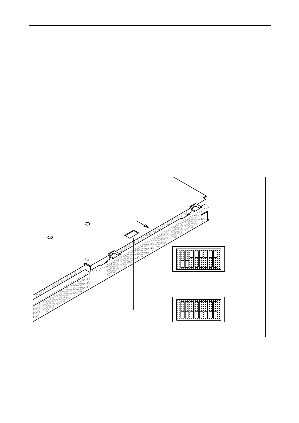
The logical address of the board can be set by changing the setting of the 8-bit DIP switch on the back of the
board (See Figure 5). The "Open" or "Off" position of a switch corresponds to a logic value of 1 and the
"Closed" or "On" position to a logic value of 0. Keep in mind that each board in the system must be assigned
its own unique logical address (if configured statically) when setting the switch.
OFF
8
1
ON
1
8
LA=3
OFF
ON
1 8
LA=255
OFF
Figure 5 - Logical Address Selection
Bustec Production Ltd. Page 13
Artisan Technology Group - Quality Instrumentation ... Guaranteed | (888) 88-SOURCE | www.artisantg.com
Page 15

ProDAQ 3150 User Manual 3150UM-01
Page 14 Bustec Production Ltd.
Artisan Technology Group - Quality Instrumentation ... Guaranteed | (888) 88-SOURCE | www.artisantg.com
Page 16
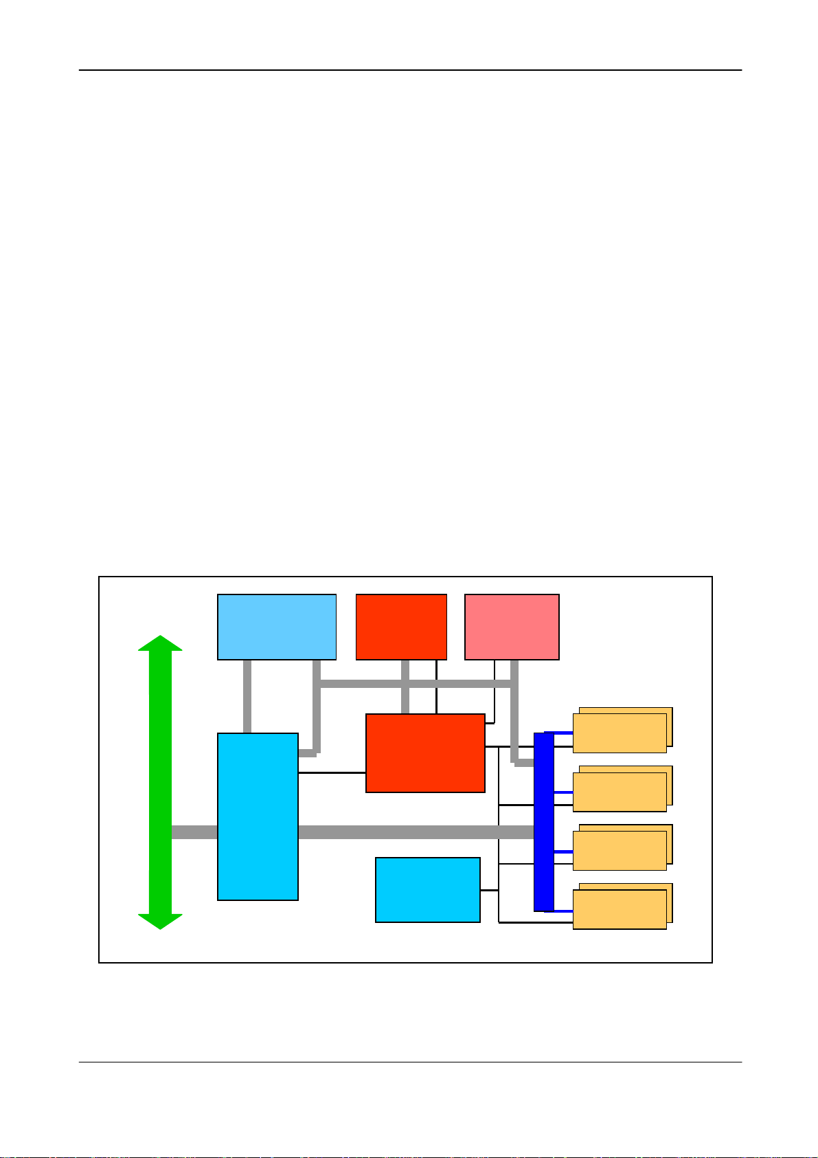
ProDAQ 3150 User Manual 3150UM-01
DSP
On-board
Communication
Voltage
V
Memory
VXIbus
Chapter 3
Theory of Operation
The ProDAQ 3150 High-Performance Motherboard is an enhanced version of the ProDAQ 3120 Standard
Motherboard. As the latter, it accepts up to eight ProDAQ function cards in a single slot, C-Size VXIbus
module, but provides in addition an enhanced VXIbus interface, an on-board processor and the option for a
DSP Plug-in module. It is function card compatible to the ProDAQ 3120 Standard Motherboard.
(2 Banks)
iBus
X
I
b
u
s
Interface
Processor
Signaling
Arbitration
Reference
(opt.)
(opt.)
FC 1/2
P
r
o
D
A
Q
B
u
s
FC 3/4
FC 5/6
FC 7/8
Bustec Production Ltd. Page 15
Figure 6 - Simplified Block Diagram
Artisan Technology Group - Quality Instrumentation ... Guaranteed | (888) 88-SOURCE | www.artisantg.com
Page 17

ProDAQ 3150 User Manual 3150UM-01
Overview
The ProDAQ 3150 Motherboard features a multi-bus architecture to optimize the data flow to/from the
ProDAQ function cards. The function cards are located on the ProDAQ bus in four stacks of two function
cards each. The ProDAQ bus can be accessed either by the VXIbus controller or from any master on the
iBus. The iBus interconnects the VXIbus controller, the memory, the on-board processor, the (optional) DSP
Plug-in Module, the internal communication registers and the ProDAQ Bus. It allows the on-board processor
and the DSP on the DSP Plug-in Module to access the function cards, the memory and the internal
communication registers.
VXIbus Interface
The VXIbus Interface Controller is responsible for handling of the VMEbus protocol, the VXIbus specific
signals, the VXI configuration registers and the access from the VXIbus to the board and it’s resources.
These resources are: the function cards, the trigger subsystem and the optional voltage reference, the
memory, the communication registers, the on-board processor and the optional DSP plug-in module.
As the ProDAQ 3120 Motherboard, the ProDAQ 3150 Motherboard allows the direct access of the function
card address space through the VXIbus interface by mapping it into the board's VXIbus address space.to
enable high data throughput, single word and block transfer access is provided. In addition a mask register,
located in the VXI configuration register set, can define a set of function cards involved in a multicast write,
or a read from multiple function cards. Broadcast write operations are also supported, to initiate a common
function in all function cards.
The ProDAQ 3150 Motherboard can be accessed from the VXIbus via byte, word, double word (32 bit) and
quad word (64 bit) access in the A32 address space. It occupies either 64 MBytes in the VXIbus A32
address space if used with 16/32MByte memory, ot 256 MByte if used with 64/128 MByte memory. In
addition to single word (either 8,16,32 bit) accesses VMEbus block transfer read and write is supported as
16 or 32 bit VME BLT transfers and 64bit MBLT transfer mode.
VXIbus Configuration registers
The VXIbus Configuration registers are located it the board's VXIbus A16 address space. The base address
fis dependent on the logical address of the motherboard, which can be selected by a the logical address
configuration switch, or if the logical address is set by this switch to 255 by software. The motherbard uses
the extended register device model, as defined by the VXI-2 Standard.
Interrupter
The VXIbus Interface Controller can generate a VXIbus interrupt on request of the on-board processor or the
processor on the optional DSP plug-in module via the internal communication registers. If a function card
want to request an interrupt, the appropriate function card trigger output line has to be routed to the interrupt
request input line of the VXIbus interface controller via the trigger switch matrix.
Page 16 Bustec Production Ltd.
Artisan Technology Group - Quality Instrumentation ... Guaranteed | (888) 88-SOURCE | www.artisantg.com
Page 18

ProDAQ 3150 User Manual 3150UM-01
Memory
The memory subsystem is organized in a dual bank fashion to allow maximum throughput to the VXIbus
system. either bank can be accessed simultaneously by both the VXIbus controller and a master on the iBus.
Which bank is accessible can be selected, so that a double-buffering scheme can be implemented to
maximize the data throughput.
On-board processor
The on-board processor controls the ProDAQ 3150 motherboard. It is responsible for initializing the
motherboard and function cards after power-up and reset, handles the communication with a host and
provides fast data-movement capabilities. It is located on the iBus and is equipt with local SRAM and FLASH
memory.
Communication/Arbitration Controller
The communication/arbitration controller provides mailbox registers for the communication between the
different masters on the motherboard and implements a resource sharing protocol. Each of the masters on
the motherboard (A VXIbus master via the VXIbus interface, the on-board processor and the optional DSP)
has two mailbox registers to communicate with the two other masters. Writing to such a mailbox register may
cause an interrupt to the corresponding master.
Arbitration is provided for access to the shared resources on the the motherboard. Shared resources are:
• the function card stacks A, B, C and D
• the trigger switch matrix interface
• the voltage reference interface
The on-board processor is by default owner of all shared resources. Other masters will have to request a
resource from the on-board processor.
Bustec Production Ltd. Page 17
Artisan Technology Group - Quality Instrumentation ... Guaranteed | (888) 88-SOURCE | www.artisantg.com
Page 19

ProDAQ 3150 User Manual 3150UM-01
The Trigger and Interrupt System
The trigger and interrupt system on the ProDAQ 3150 Motherboard is build using a programmable trigger
switch matrix. The switch matrix allows to connect all trigger sources and sinks available:
Function Card Trigger Outputs
Each function card features one trigger output line, allowing the function card to send a
trigger to the switch matrix.
Function Card Trigger Inputs
Each function card features one trigger input line, which can be used to send trigger or clock
signals to the function card.
VXIbus TTL/ECL Trigger Lines
The VXIbus TTL/ECL trigger lines can be used to send or receive trigger signals from other
VXIbus devices or the controller.
VXIbus Interface
The VXIbus interface features one trigger input line, which can be used to generate an
VXIbus interrupt.
The clock signals for the function cards are also routed via the switch matrix to allow them to be shut off in
case no function card is fitted to a slot.
The switch matrix can be programmed to connect two or more of those sinks and sources together, so
that for example
• a function card output trigger line can be routed to a VXIbus trigger line
• a VXIbus trigger line can be routed to a function card trigger input line
• a function card trigger output line can be routed to a function card trigger input line
• a function card trigger output line can be routed to the VXIbus interface to generate an
interrupt.
Page 18 Bustec Production Ltd.
Artisan Technology Group - Quality Instrumentation ... Guaranteed | (888) 88-SOURCE | www.artisantg.com
Page 20
ProDAQ 3150 User Manual 3150UM-01
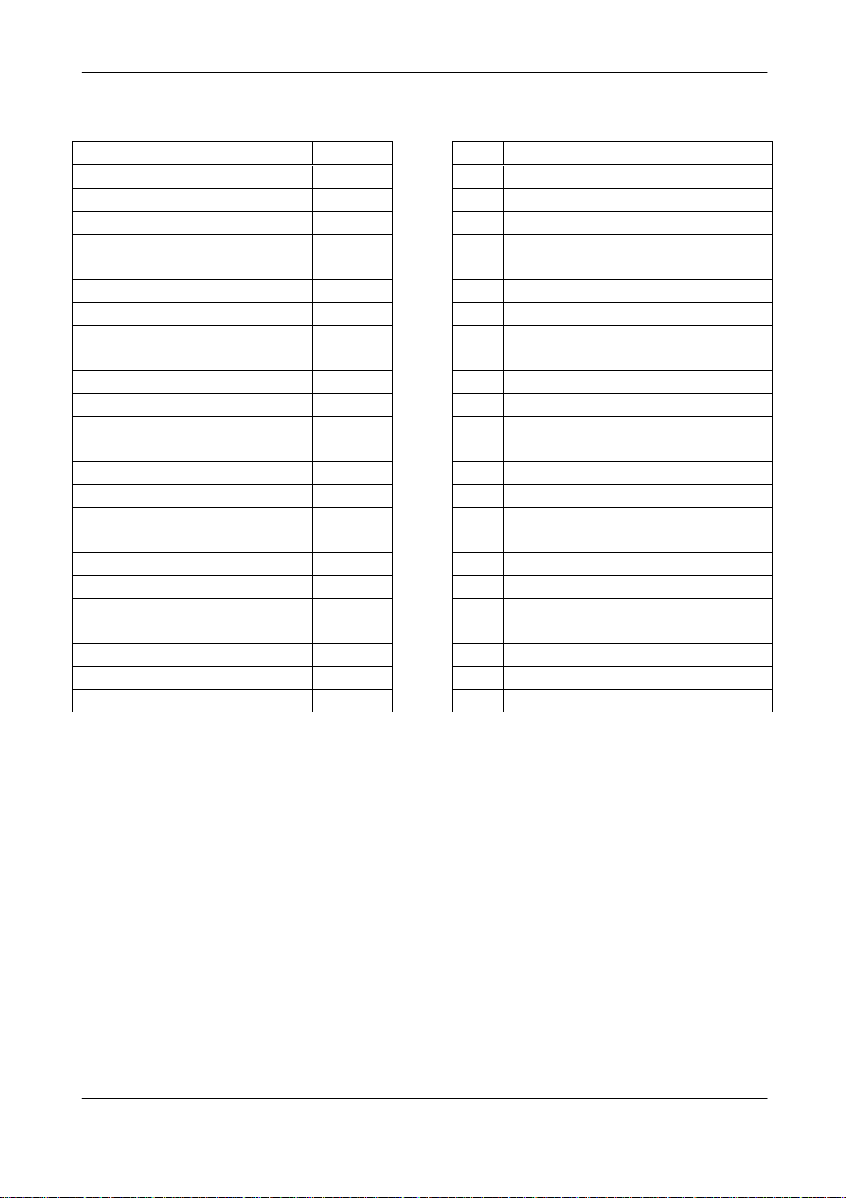
Port Function Direction Port Function Direction
0 FC 1 Trigger Input Out 24 VXIbus TTL Trigger Line 2 Out
1 FC 2 Trigger Input Out 25 FC 4 Clock Out
2 FC 3 Trigger Input Out 26 FC 3 Clock Out
3 FC 4 Trigger Input Out 27 VXIbus TTL Trigger Line 3 Out
4 FC 5 Trigger Input Out 28 VXIbus TTL Trigger Line 4 Out
5 FC 6 Trigger Input Out 29 FC 2 Clock Out
6 FC 7 Trigger Input Out 30 FC 1 Clock Out
7 FC 8 Trigger Input Out 31 VXIbus TTL Trigger Line 5 Out
8 FC 1 Trigger Output In 32 VXIbus TTL Trigger Line 6 Out
9 FC 2 Trigger Output In 33 VXIbus TTL Trigger Line 7 Out
10 FC 3 Trigger Output n 34 VXIbus TTL Trigger Line 0 In
11 FC 4 Trigger Output In 35 VXIbus TTL Trigger Line 1 In
12 FC 5 Trigger Output In 36 VXIbus TTL Trigger Line 2 In
13 FC 6 Trigger Output In 37 VXIbus TTL Trigger Line 3 In
14 FC 7 Trigger Output In 38 VXIbus TTL Trigger Line 4 In
15 FC 8 Trigger Output In 39 VXIbus TTL Trigger Line 5 In
16 MB Base Clock (40 MHz) In 40 VXIbus TTL Trigger Line 6 In
17 FC 8 Clock Out 41 VXIbus TTL Trigger Line 7 In
18 FC 7 Clock Out 42 SYSCLK (16 MHz) In
19 MB Base Clock 2 In 43 VXIbus ECL Trigger Line 0 In
20 VXIbus TTL Trigger Line 0 Out 44 CLK10 (10 MHz) In
21 FC 6 Clock Out 45 VXIbus ECL Trigger Line 1 In
22 FC 5 Clock Out 46 CLK/2 (20 MHz) In
23 VXIbus TTL Trigger Line 1 Out 47 VXIbus Interface LLIRQ* Out
Table 1 - The In/Output Ports of the Switch Matrix
In general 1:m as well as n:1 connections are possible, with some limitations on the type of lines involved in
the connection and the number of lines connected. Table 1 shows a complete list of signals connected to the
switch matrix. Because of the drivers involved to drive the trigger signals on the VXIbus, the VXIbus trigger
lines appear each as two signals, one input and one output, in the list.
The trigger and interrupt system is programmed via five registers, two in the VXIbus configuration register set
(IRQH and JTAG) and three registers located in the boards A24/A32 space.
Bustec Production Ltd. Page 19
Artisan Technology Group - Quality Instrumentation ... Guaranteed | (888) 88-SOURCE | www.artisantg.com
Page 21

ProDAQ 3150 User Manual 3150UM-01
Page 20 Bustec Production Ltd.
Artisan Technology Group - Quality Instrumentation ... Guaranteed | (888) 88-SOURCE | www.artisantg.com
Page 22

ProDAQ 3150 User Manual 3150UM-01
Chapter 4
Programming Information
VXIbus Interface and Registers
The VXIbus Interface conforms to the VXIbus specification issue 1.4. In addition to a static VXI device
configuration, it supports dynamic configuration. It is a register-based device, which supports A16/A32
addressing, and requires 16 Mbytes from the A32 address space.
To access the function cards it is necessary to set the modules A32 base address in the offset register.
The module responds to the following AM codes:
AM = 0x29 or 0x2d short IO (A16) for VXIconfig.
AM = 0x0e or 0x0d or 0x0a or 0x09 normal A32 access
AM = 0x0b or 0x0f for A32 block transfers
AM = 0x08 or 0x0c for A32/D64 MBLT transfers
Access to the module is with byte, word, double word and quad word transfers. Unaligned data transfer, i.e.
access to byte 1,2 or 1,2,3 or 0,1,2 is not supported. The module will respond with a bus error to such a
transfer request.
A data transfer to a valid local address is timed out after 25.6 µsec with a BERR signal if the FBus does not
respond. This feature is programmable (direct BERR or wait until internal timeout). In cases where the
internal resources are explicitly locked a BERR is generated immediately.
Bustec Production Ltd. Page 21
Artisan Technology Group - Quality Instrumentation ... Guaranteed | (888) 88-SOURCE | www.artisantg.com
Page 23

ProDAQ 3150 User Manual 3150UM-01
VXIbus Configuration Registers
All addresses are shown as an offset to the base of the motherboards logical address space.
Address Mnemonic OP
0x00 Config RO VXI device type and manufacturer ID = 5E70
0x00 LogAdr WO VXI device logical address
0x02 DevID RO device ID and addr. space requirement = 5C4E (32MB) or 3C4E (128MB)
0x04 Status ROC general and device specific status information
0x04 Control WOC general and specific control
0x06 Offset RW A32 address space offset
0x08 Attribute RO Attribute Register = 0002
0x0A SerNumHigh RWO Fetched from EEPROM by software
0x0C SerNumLow RWO Fetched from EEPROM by software
0x0E Version RO Firmware/Hardware version
0x10 RO reserved
0x12 RO reserved
0x14 RO reserved
0x16 RO reserved
0x18 RO reserved
0x1A InterStatus RO Interrupt Status
0x1C InterControl RW Interrupt Control
0x1E SubClass RO Extended Subtype= FFFE
0x20 FC_AVAIL_RESET RW reset-control of function cards and status of AVAIL bits
0x22 MB_LIST RW Mailbox: VXItoLIST and LISTtoVXI (16 bit)
0x24 MB_DSP RW Mailbox: VXItoDSP and DSPtoVXI (16 bit)
0x26 MB_STATUS R Mailbox STATUS register
0x28 JTAG RW JTAG interface for switch matrix loading
0x2a FCMOD RW FC-CLK disable
0x2c FCMASK RW pattern mask for selecting concurrent write
0x2e VXI_TRIG_OUT RW VXI Trigger SET and status register (TM2..0, FC_TRIG_IN0..7)
0x30 EEPROM_CTRL RW Read/Write control of three serial EEPROMS (mother board, LIST, DSP)
0x32 LIST_DSP_CTRL RW reset and boot control of LIST-processor and DSP
0x34 FCADR RO last address send to the function cards
0x36 UTIL RW serial EEPROM select bits and SYSFAIL Test bit
0x38 FC_STACK_LOCK_SET RW Software FC-Card Stack arbitration register (Set Request)
0x3A FC_STACK_LOCK_CLR W Software FC-Card Stack arbitration register (Release)
0x3C SOURCE_ARB_SET RW Software board register arbitration register
0x3E SOURCE_ARB_CLR W Software board register arbitration register
Page 22 Bustec Production Ltd.
Artisan Technology Group - Quality Instrumentation ... Guaranteed | (888) 88-SOURCE | www.artisantg.com
Page 24
ProDAQ 3150 User Manual 3150UM-01
VXIbus Configuration Register Details
The following describes the device specific configuration register bits in detail.
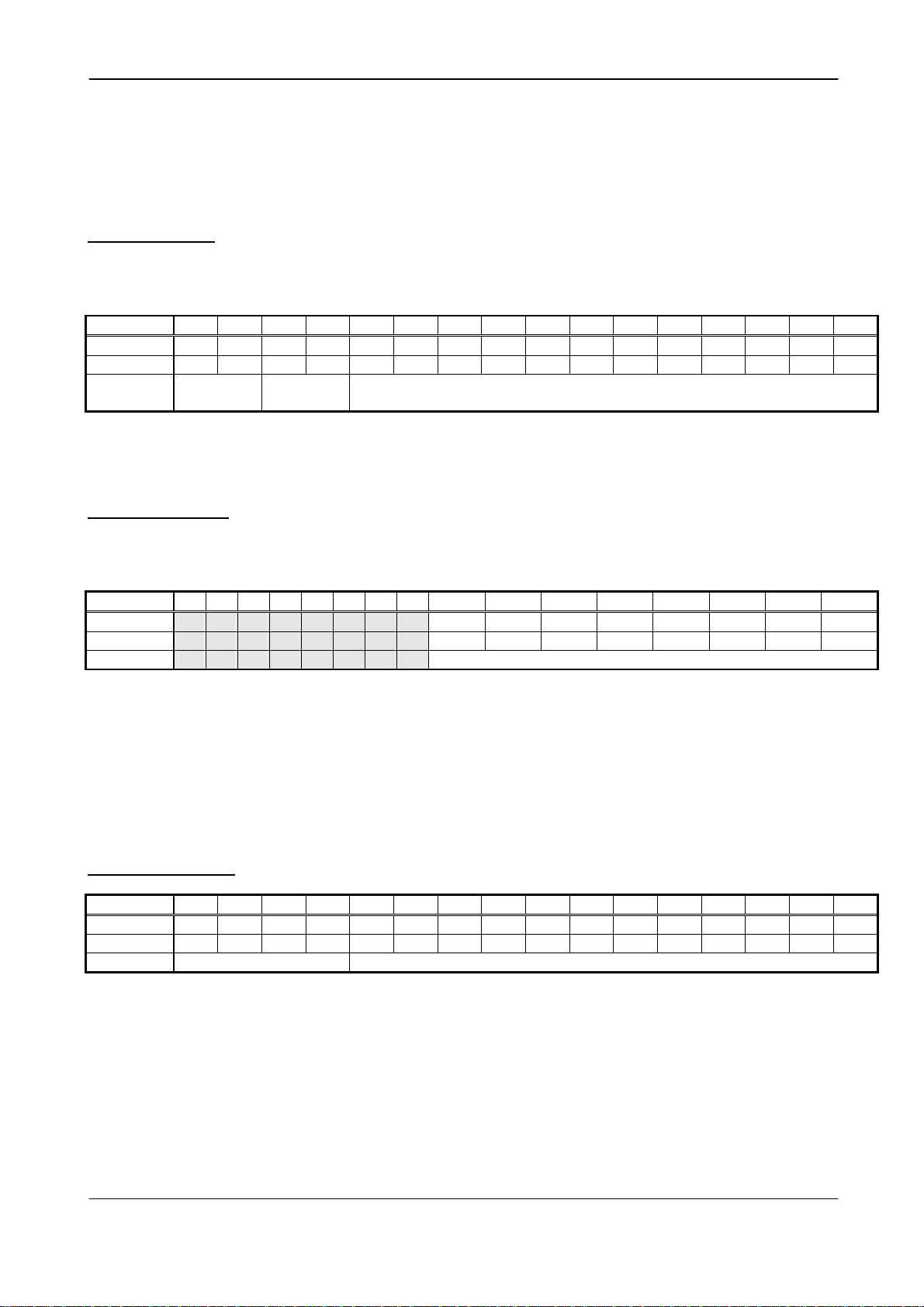
Config (0x0 read)
This register provides information about the device class, the address space and the manufacturer ID of
the module.
Bit 15 14 13 12 11 10 9 8 7 6 5 4 3 2 1 0
Operation RO RO RO RO RO RO RO RO RO RO RO RO RO RO RO RO
Initial 0 1 0 1 1 1 1 1 1 1 1 1 1 0 1 1
Name
LogAdr (0x0, write)
If the module is configured for dynamical logical address assignment, this register can be used to set
its logical address.
Bit 15 14 13 12 11 10 9 8 7 6 5 4 3 2 1 0
Operation WO WO WO WO WO WO WO WO
Initial LA-8 LA-7 LA-6 LA-5 LA-4 LA-3 LA-2 LA-1
Name LogAdr
Device
Class
Device Class: 01 - Extended
Address Space: 01 - A16 / A32
Manufacturer ID: 0xE70 - Bustec Production Ltd.
Address
Space
Manufacturer ID
If all switches of the logical address switch are off (correspond to static address 255), the
device acts as a dynamically configurable VXIbus device, and a write to this register
changes the logical address. If any other address then 255 is choosen by setting the logical
address switch, the device acts as a static configured VXIbus device and a write to this
register has no effect.
After a write operation, the new logical address becomes available when the access cycle
has finished (approx. 150ns after end of the selection).
DeviceID (0x2, read)
Bit 15 14 13 12 11 10 9 8 7 6 5 4 3 2 1 0
Operation RO RO RO RO RO RO RO RO RO RO RO RO RO RO RO RO
Initial x x x x 1 1 0 0 0 1 0 0 1 1 1 0
Name Required Memory Model ID
Required Memory: 0101 - 64MB (If 16MB DRAM Modules are used)
0011 - 256MB (If 64MB DRAM Modules are used)
Model ID: 0xC4E - ProDAQ 3150
The memory size will be automatically detected by the hardware during initialization. If one of
the memory banks is equipped with a 64MB module, the memory size will be automatically
256MB.
Bustec Production Ltd. Page 23
Artisan Technology Group - Quality Instrumentation ... Guaranteed | (888) 88-SOURCE | www.artisantg.com
Page 25
ProDAQ 3150 User Manual 3150UM-01
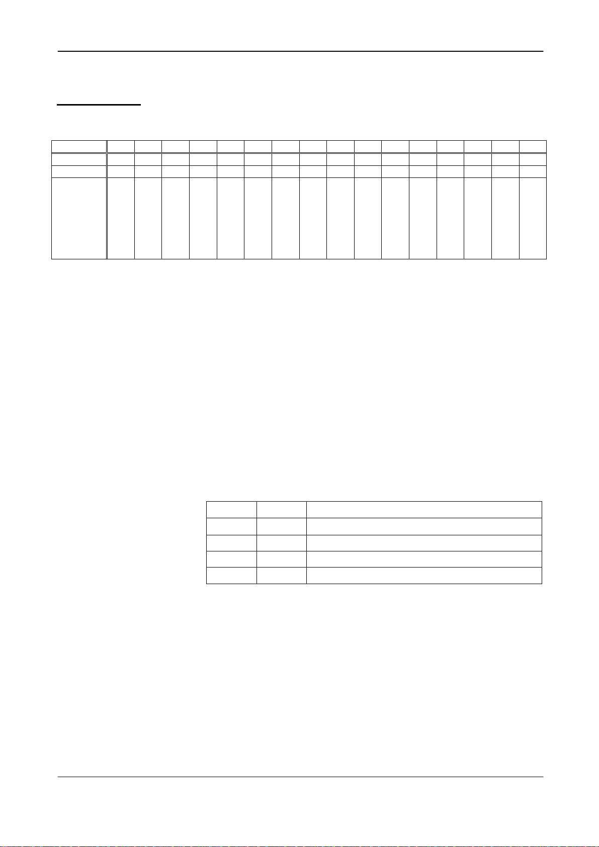
Status (0x4, read)
Indicates the module status:
Bit 15 14 13 12 11 10 9 8 7 6 5 4 3 2 1 0
Operation
Initial 0 0 0 0 0 0 0 0 0 0 0 0 1 1 0 0
Name
RW RO RO RO RO RO RO RO RO RO RO RO RO RO RW RW
PDB7
PDB6
PDB7
reserved
A32 enable
VXI Modid_L
reserved
reserved
InterPend
DRAM Bank 2
DRAM Bank 2
PDB6
DRAM Bank 1
VOFF_SET
DRAM Bank 1
Ready
RLOG_SET
SysFail
Passed
Reset
Reset indicates the reset state of the module
Sysfail indicates the status of the VXIbus SysFail line
Passed Internal Selftest has passed (FPGAs are ready)
Ready after the state machines are initialized
RLOG_SET read as 1 if the logical address is set
VOFF_SET read as 1 if the A32 offset address is set
PDB6 DRAM Bank 1 memory ID bit 6 Bank1 (upper 72-pin SO-DIMM)
PDB7 DRAM Bank 1 memory ID bit 7 Bank1 (upper 72-pin SO-DIMM)
PDB6 DRAM Bank 2 memory ID bit 6 Bank2 (lower 72-pin SO-DIMM)
PDB7 DRAM Bank 2 memory ID bit 7 Bank2 (lower 72-pin SO-DIMM)
PDB7 PDB6 assign
0 0 reserved
0 1 16 MByte SO-Dimm
1 0 64 MByte SO-Dimm
1 1 not inserted
InterPend VXI Interrupt Pending
MODID_L 0 indicates the modules is selected with the MODID line active
A32 Enable read as 1 if access via the A32 address space is allowed
Page 24 Bustec Production Ltd.
Artisan Technology Group - Quality Instrumentation ... Guaranteed | (888) 88-SOURCE | www.artisantg.com
Page 26
ProDAQ 3150 User Manual 3150UM-01
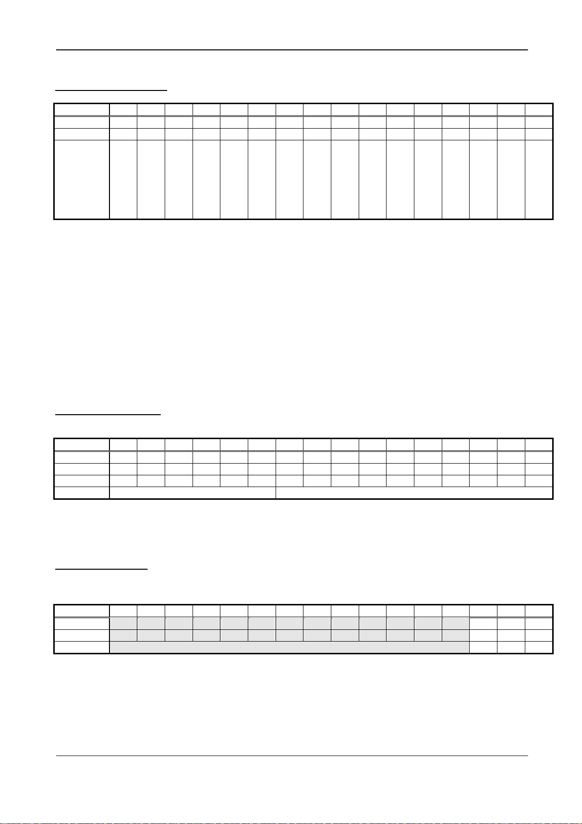
Control (0x4, read/write)
Bit 15 14 13 12 11 10 9 8 7 6 5 4 3 2 1 0
Operation RW RO RO RO RO RO RO RO RO RO RO RO RO RO RW RW
Initial 0 0 0 0 0 0 0 0 0 0 0 0 0 0 0 0
Name
reserved
reserved
reserved
reserved
reserved
reserved
reserved
reserved
reserved
reserved
reserved
reserved
A32 Enable
RESET writing a 1 resets the device (clears configuration registers, aborts all
operations)
SYSFAIL Inhibit disables the device from driving the SYSFAIL_L line. By default Resource
Managers set this bit to 0.
reserved
Inhibit
VXI SYSFAIL
A32 Enable write of 1 will enable the A32 addressing mode, a 0 will disable the A32
addressing.
Note: The offset register has to be set up before A32 access is enabled.
Any attempt to enable the A32 addressing mode without prior offset
register configuration will fail.
Offset (0x6, read/write)
Bit 15 14 13 12 11 10 9 8 7 6 5 4 3 2 1 0
Operation RW RW RW RW RW RW RO RO RO RO RO RO RO RO RO RO
Initial 0 0 0 0 0 0 0 0 0 0 0 0 0 0 0 0
Compare A31 A30 A29 A28 A27 A26
Name Offset 0
Defines the offset of the boards address space in the VXIbus address space. Depending on
the configuration the board uses 64 or 256 MByte in the VXIbus A32 address space.
Attribute (0x8, read)
Defines the capability of the module to send and to receive Interrupts.
Bit 15 14 13 12 11 10 9 8 7 6 5 4 3 2 1 0
Operation RO RO RO
Initial 0 1 0
Name Not implemented IR* IH* IS*
IS Interrupt Status Register (is implemented)
IH Interrupt Handler Controller Capability (not implemented)
IR Interrupt Controller (is implemented), allows the module to send VXIbus interrupts.
RESET
Bustec Production Ltd. Page 25
Artisan Technology Group - Quality Instrumentation ... Guaranteed | (888) 88-SOURCE | www.artisantg.com
Page 27

ProDAQ 3150 User Manual 3150UM-01
SerialLow (0xB, read/write) and SerialHigh (0xA, read/write)
Holds the Serial Number of the module. The contents is copied by software from the serial EEPROM into the
registers.
Bit 15 14 13 12 11 10 9 8 7 6 5 4 3 2 1 0
Operation RWO RWO RWO RWO RWO RWO RWO RWO RWO RWO RWO RWO RWO RWO RWO RWO
Initial 0 0 0 0 0 0 0 0 0 0 0 0 0 0 0 0
Name
Version (0xE, read only)
This defines the hardware and firmware revision of the module
Bit 15 14 13 12 11 10 9 8 7 6 5 4 3 2 1 0
Operation RO RO RO RO RO RO RO RO RO RO RO RO RO RO RO RO
Initial 0 0 0 1 0 0 0 1 0 0 0 1 0 0 0 1
Name Firmware Main Version
InterStatus (0x1A, read)
Bit 15 14 13 12 11 10 9 8 7 6 5 4 3 2 1 0
Operation RO RO RO RO RO RO RO RO RO RO RO RO RO RO RO RO
Initial 0 0 0 0 0 0 0 0 0 0 0 0 0 0 0 0
Name
SW
Cause/ Status
Firmware Revision Hardware Main Version Hardware Revision
MBX
DSP
Serial Number
MBX
LP
TM
LogAddress
TM Interrupt is caused by a request from the trigger switch matrix.
MBX LP Interupt Request from the LP -> VXI mailbox register.
MBX DSP Interrupt Request from the DSP -> VXI mailbox register.
SW Interrupt caused by SW (for testing only)
To figure out which is the real cause of the interrupt, the software has to read the
TriggerStatusR register if the FC bit is set, or the mailbox registers if any of the other bits are
set.
Page 26 Bustec Production Ltd.
Artisan Technology Group - Quality Instrumentation ... Guaranteed | (888) 88-SOURCE | www.artisantg.com
Page 28
ProDAQ 3150 User Manual 3150UM-01
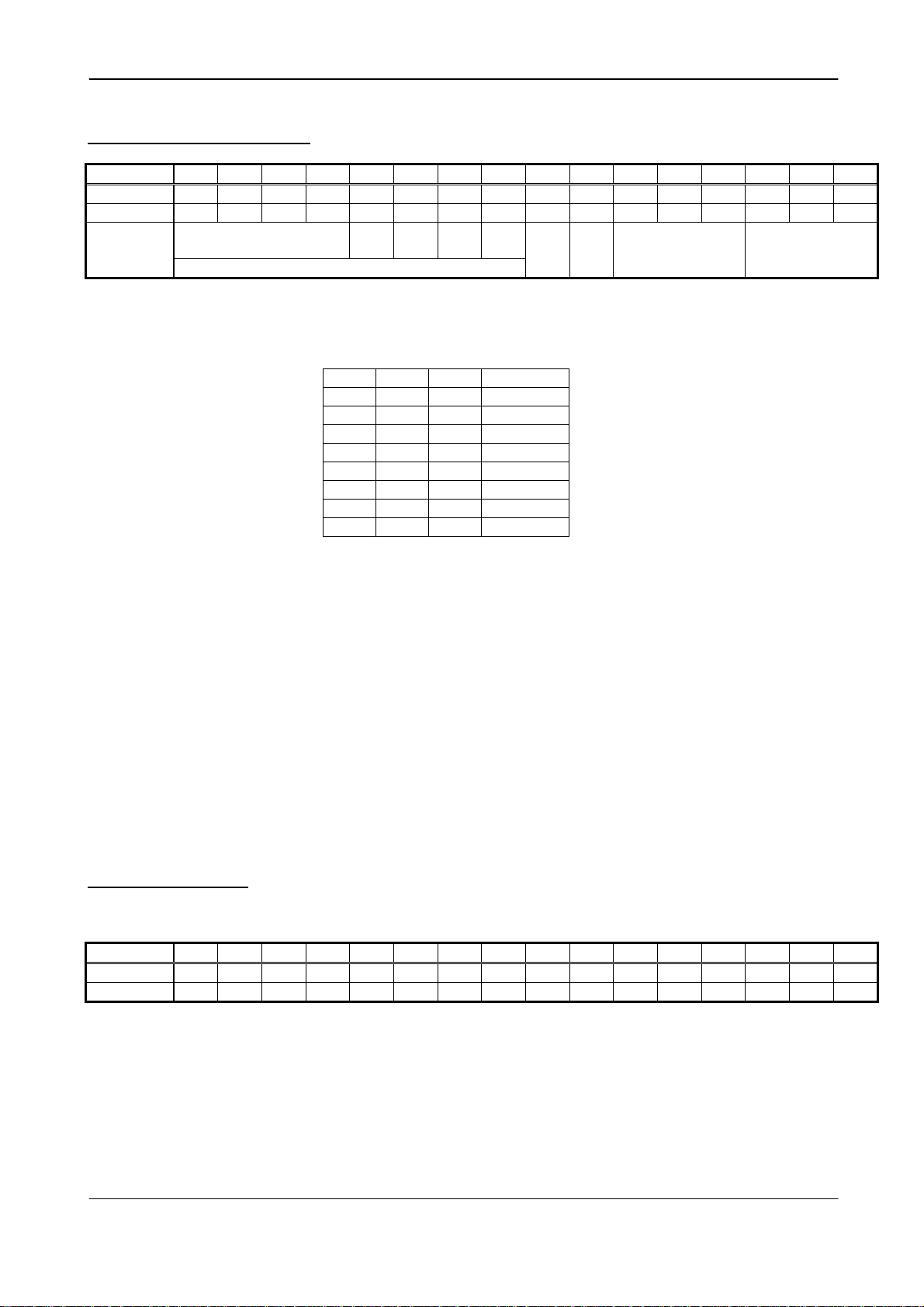
InterControl (0x1C, read/write)
Bit 15 14 13 12 11 10 9 8 7 6 5 4 3 2 1 0
Operation RO RO RO RO RO RW RW RW RW RO RW RW RW RO RO RO
Initial 1 1 1 1 1 1 1 1 1 1 1 1 1 1 1 1
MBX
Name
Not used SW
Interrupt Mask
DSP
MBX
LP
TM
IR
ena*
IH
ena*
Interrupt IRQ
Line*
Handler IRQ
Line*
Handler IRQ Line not used, permanently 7
Interrupt IRQ Line* selects a interrupt line on the VXI/VMEbus
Bit 5 Bit 4 Bit 3 IRQ Line
0 0 0 IRQ7
0 0 1 IRQ6
0 1 0 IRQ5
0 1 1 IRQ4
1 0 0 IRQ3
1 0 1 IRQ2
1 1 0 IRQ1
1 1 1 disabled
IH ena* Interrupt Handler enable, permanently 1 (disable)
IR ena* Interrupter enable, 1-disables, 0 enabled.
Interrupt Mask enable mask, enabled if bit is set to 0
TM enables interrupt requests from the trigger switch matrix.
MBX LP enables interrupt requests from the LP -> VXI mailbox register.
MBX DSP enables interrupt requests from the DSP -> VXI mailbox register.
SW causes an interrupt by writing a 0 (for testing only).
Note: a Hard reset (power up, SYSRESET) and a soft reset (reset via the control register)
resets the content of the programmable bits into the initial state.
Subclass (0x1E, read)
Defines the VXIbus definition of the sub classes. This module is extended register.
Bit 15 14 13 12 11 10 9 8 7 6 5 4 3 2 1 0
Operation RO RO RO RO RO RO RO RO RO RO RO RO RO RO RO RO
Initial 1 1 1 1 1 1 1 1 1 1 1 1 1 1 1 0
Bustec Production Ltd. Page 27
Artisan Technology Group - Quality Instrumentation ... Guaranteed | (888) 88-SOURCE | www.artisantg.com
Page 29

ProDAQ 3150 User Manual 3150UM-01
FC_AVAIL_RESET (0x20, read/write)
Reset function cards, the List Processor, the memories and the optional DSP
Bit 15 14 13 12 11 10 9 8 7 6 5 4 3 2 1 0
Initial 0 0 0 0 0 0 0 0
read
function
FC8 AVAIL
FC7 AVAIL
FC6 AVAIL
FC5 AVAIL
FC4 AVAIL
FC3 AVAIL
FC2 AVAIL
FC1 AVAIL
FC 8
FC 7
FC 6
FC 5
FC 4
FC 3
FC 2
ENABLE/RESET
ENABLE/RESET
ENABLE/RESET
ENABLE/RESET
ENABLE/RESET
ENABLE/RESET
ENABLE/RESET
write
res
res
res
res
res
res
res
function
res
FC 8
FC 7
FC 6
FC 5
FC 4
FC 3
FC 2
ENABLE/RESET
ENABLE/RESET
ENABLE/RESET
ENABLE/RESET
ENABLE/RESET
ENABLE/RESET
ENABLE/RESET
FC1 ... FC8 AVAIL signals availability of the corresponding front end card
read:
ENABLE FC1 ... FC8 reflects the ENABLE/RESET status of the corresponding front end card
write:
ENABLE FC1 ... FC8 drive directly the reset lines to the function card located at the specific
position. To enable the function cards a 1 has to be written.
MB_LP (0x22, read/write)
The MAIILBOX register set (MB_LP) consists of two 16-bit registers:
MB_LP_TO_VXI (read) and
MB_VXI_TO_LP (write)
A write to this mailbox register sets a bit in the MB_STATUS register and causes (if enabled) an interrupt to
the destination, which is cleared after the destination processor has read the message register.
FC 1
ENABLE/RESET
FC 1
ENABLE/RESET
MB_DSP (0x24, read/write)
A write to this mailbox register sets a bit in the MB_STATUS register and causes (if enabled) an interrupt to
the destination, which is cleared after the destination processor has read the message register.
The MAIILBOX register set (MB_LIST) consists of two 16-bit registers:
MB_DSP_TO_VXI (read) and
MB_VXI_TO_DSP (write)
Page 28 Bustec Production Ltd.
Artisan Technology Group - Quality Instrumentation ... Guaranteed | (888) 88-SOURCE | www.artisantg.com
Page 30
ProDAQ 3150 User Manual 3150UM-01
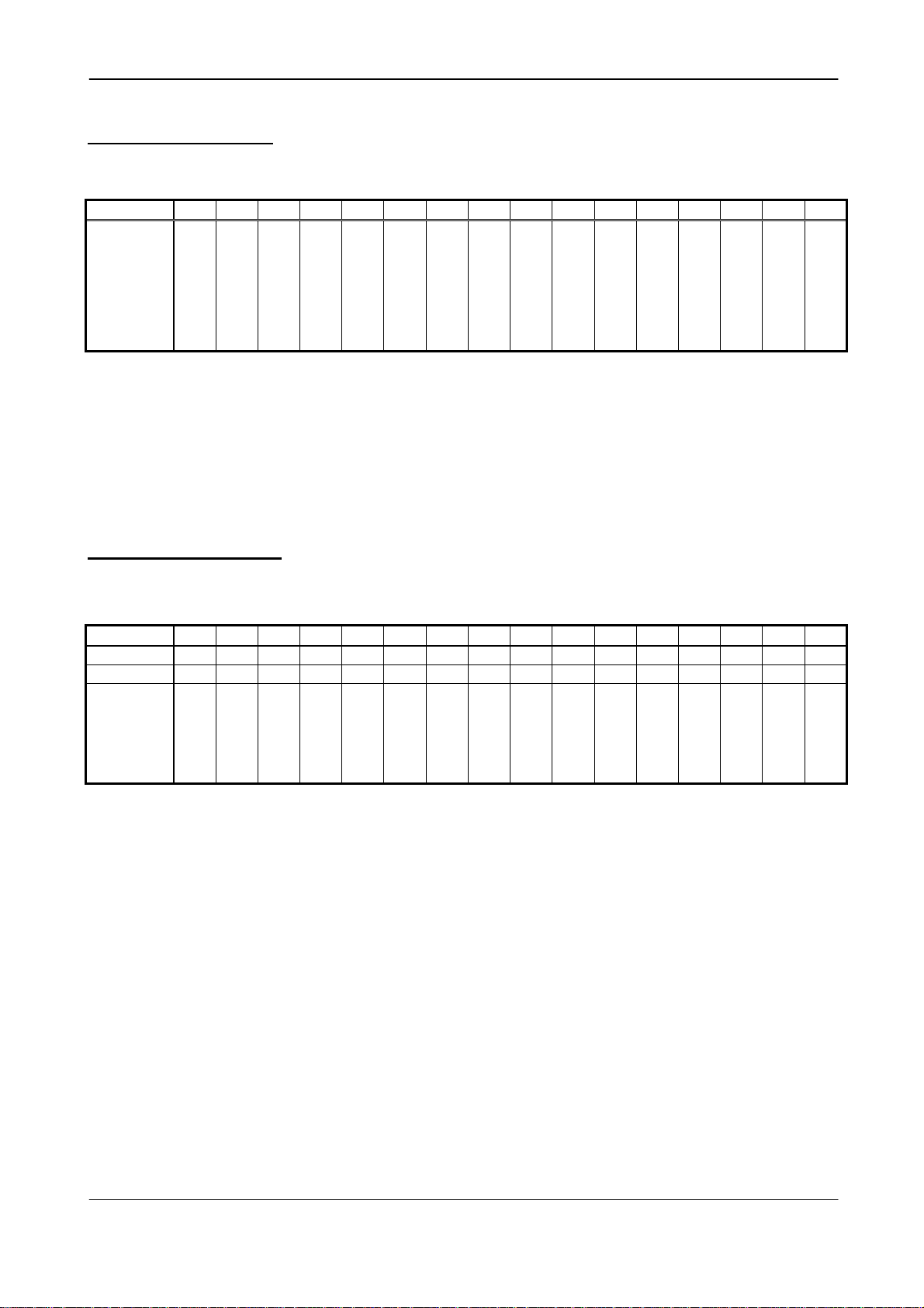
MB_STATUS (0x26, read)
(bit assignments like list processor register MB_STATUS)
Bit 15 14 13 12 11 10 9 8 7 6 5 4 3 2 1 0
Function 0 0 0 0 0 0
0 0
0 0
sLPtoDSP
sVXItoDSP
sLPtoVXI signals message in LP to VXI mailbox register
sDSPtoVXI signals message in DSP to VXI mailbox register
sVXItoLP signals message in VXI to LP mailbox register
sDSPtoLP signals message in DSP to VXI mailbox register
sVXItoDSP signals message in VXI to DSP mailbox register
sLPtoDSP signals message in LP to DSP mailbox register
sVXItoLP
sDSPtoLP
sDSPtoVXI
IQ-JTAG (0x28, read/write)
A simple JTAG interface is used to load and modify the switch matrix.
Bit 15 14 13 12 11 10 9 8 7 6 5 4 3 2 1 0
Operation RW RW RW RW RW RW RW RW RW RW RW RW RW RW RW RW
Initial 0 0 0 0 0 0 0 0 0 0 0 0 0 0 0 0
Name
SW1
RCena
TSMena
VXITOena
SW0
JTLOC
TDI
TDO
TMS*
TCLK
sLPtoVXI
TRST*
TRST* reset of the Trigger Switch Matrix JTAG interface. For a proper reset write a 1
and after >100µs a 0 into that register bit.
TCLK JTAG clock, Note: a clock pulse is generated automatically (75 ns) if a 1 is
written into that register
TMS to change the state machine (output is inverted)
TDI (inverted data input for JTAG device)
TDO (data output)
JTLOC enable JTAG interface
SW0 - used by SW
SW1 - used by SW
VXITOena - Enable Trigger output to VXI bus. A one has to be written in to enable the
output.
TSMena - Enables the output from the Trigger Switch Matrix. A one has to be written in
to enable the output. Signal gets inverted to provide the right polarity. At
startup the output is disabled.
RCena - Rapid Connect enable (low active). A one has to be written in to enable the
output.
Bustec Production Ltd. Page 29
Artisan Technology Group - Quality Instrumentation ... Guaranteed | (888) 88-SOURCE | www.artisantg.com
Page 31
ProDAQ 3150 User Manual 3150UM-01
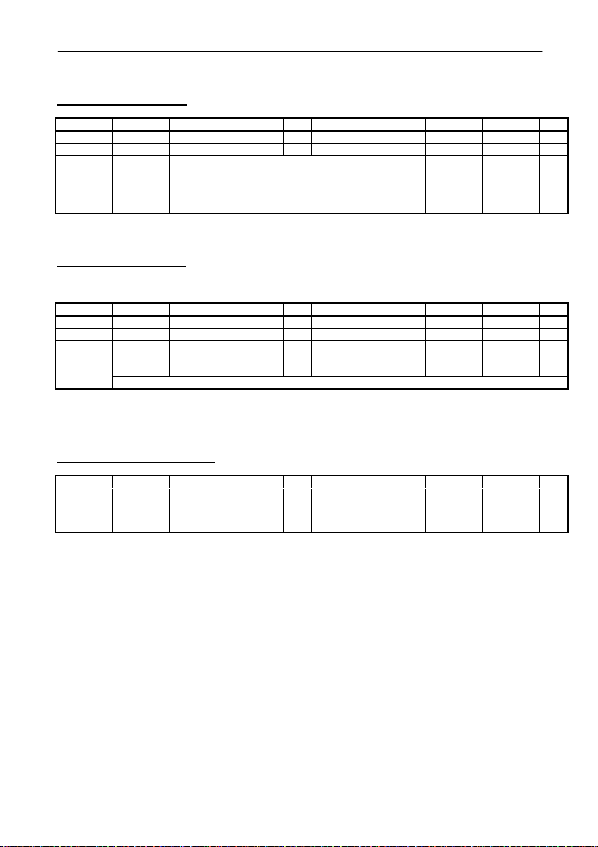
FCMODE (0x2A, read/write)
Bit 15 14 13 12 11 10 9 8 7 6 5 4 3 2 1 0
Operation RO RO RO RO RO RO RO RO RW RW RW RW RW RW RW RW
Initial 0 0 0 0 0 0 0 0 0 0 0 0 0 0 0 0
Name
Disable
Disable
Disable
Disable
Disable
Disable
FC8_CLK
FC7_CLK
FC6_CLK
FC5_CLK
FC4_CLK
FC3_CLK
Disable
FC2_CLK
FC_CLK disable disables the FC-card clock
FCMASK (0x2C, read/write)
Used for broadcast write operations and concurrent Read/write operations.
Bit 15 14 13 12 11 10 9 8 7 6 5 4 3 2 1 0
Operation RW RW RW RW RW RW RW RW RW RW RW RW RW RW RW RW
Initial 0 0 0 0 0 0 0 0 0 0 0 0 0 0 0 0
Disable
FC1_CLK
Name
FC 8
FC 7
FC 6
FC 5
FC 4
FC 3
FC 2
FC 1
FC 8
FC 7
FC 6
FC 5
FC 4
FC 3
FC 2
Read mask Write mask
Bit 15 8 used to indicate selected channels for read,
Bit 7 0 selected channels for write operation
VXI_TRIG_OUT (0x2E, read/write)
Bit 15 14 13 12 11 10 9 8 7 6 5 4 3 2 1 0
Operation R R R R R RW RW RW RW RW RW RW RW RW RW RW
Initial 0 0 0 0 0 0 0 0 0 0 0 0 0 0 0 0
Name
Read: FCTI 0 … 7 Status of the Function card trigger input
(actual level; “0” : active; “1” : not active)
TMO 0 … 2 Status of the trigger line from the communication registers to the trigger
matrix
(actual level; “0” : active; “1” : not active)
Write: FCTI 0 … 7 “1” : set the Function card trigger input (set to low)
“0”: clear the Function card trigger input (tristate)
TMO 2 TMO 1 TMO 0 FCTI 7 FCTI 6 FCTI 5 FCTI 4 FCTI 3 FCTI 2 FCTI 1 FCTI
FC 1
0
TMO 0 … 2 “1” : set the trigger line from the VXI communication register to the trigger
matrix (set to low)
“0” : clear the trigger line from the VXI communication register to the trigger
matrix (tristate)
Page 30 Bustec Production Ltd.
Artisan Technology Group - Quality Instrumentation ... Guaranteed | (888) 88-SOURCE | www.artisantg.com
Page 32
ProDAQ 3150 User Manual 3150UM-01
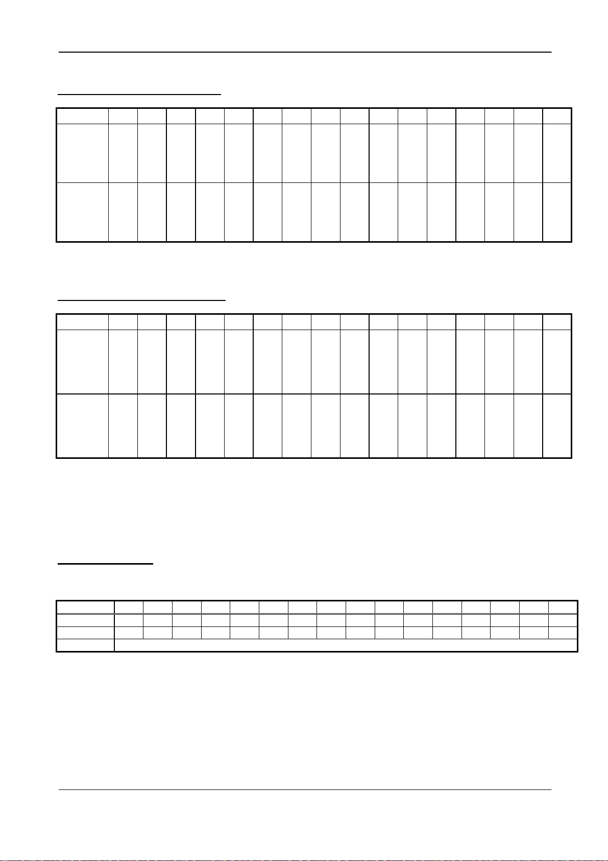
EEPROM_CTRL (0x30, read/write)
Bit 15 14 13 12 11 10 9 8 7 6 5 4 3 2 1 0
Write
res
res
res
res
Function
Read
Function
cmd
cmd
cmd
READ
WRITE
RESET
0
0
0
0
BUSY
Present
res
wdata 7
wdata 6
wdata 5
wdata 4
wdata 3
wdata 2
res
res
rdata 7
rdata 6
rdata 5
rdata 4
rdata 3
rdata 2
LIST_DSP_CTRL (0x32, read/write)
Bit 15 14 13 12 11 10 9 8 7 6 5 4 3 2 1 0
Write
M1
Function
Read
Function
res
res
res
res
res
DSP
RESET
DSP Boot
(2)
0
0
0
DSP
AVAIL
DSP
SW701_2
RESET
DSP Boot
M0
res
res
res
res
res
LIST
DSP Boot
0
0
M1
M0
DSP Boot
0
LIST
AVAIL
SW701_1
RESET
(1)
LIST
RESET
wdata 1
wdata 0
rdata 1
rdata 0
M1
M0
LIST Boot
LIST Boot
M1
M0
LIST Boot
LIST Boot
(1)
With switch SW701_1 open (high) RESET condition after power up, with switch closed RUN condition after
power up
(2)
With switch SW701_2 open (high) RESET condition after power up, with switch closed RUN condition after
power up
FCADR (0x34, read)
Production use only.
Bit 15 14 13 12 11 10 9 8 7 6 5 4 3 2 1 0
Operation RO RO RO RO RO RO RO RO RO RO RO RO RO RO RO RO
Initial 0 0 0 0 0 0 0 0 0 0 0 0 0 0 0 0
Name FCADR[15:0]
Bustec Production Ltd. Page 31
Artisan Technology Group - Quality Instrumentation ... Guaranteed | (888) 88-SOURCE | www.artisantg.com
Page 33
ProDAQ 3150 User Manual 3150UM-01
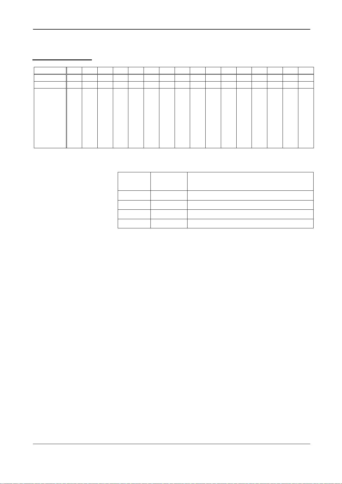
Util (0x36, read/write)
Bit 15 14 13 12 11 10 9 8 7 6 5 4 3 2 1 0
Operation RO RO RO RO RO RO RO RO RO RO RO RO RW RW RW RW
Initial 0 0 0 0 0 0 0 0 0 0 0 0 0 0 0 0
Name
EEPRM SELn Selects which EEPROM is accessible via the EEPRM_CTRL register.
res
res
res
res
res
res
res
res
res
res
res
VME_OREDER
VME_BLOCK_PIPE
(Test)
SYSFAIL OUT
EEPRM SEL1
EEPRM
SEL1
EEPRM
SEL1
access to/from
0 0 Motherboard EEPROM
EEPRM SEL0
0 1 Motherboard EEPROM
1 0 LIST EEPROM
1 1 DSP EEPROM
SYSFAIL OUT Test flag to generate a VME SYSFAIL signal (if enabled)
VME_ORDER controls the 16-bit word order during a D32/BLT32 access to or from the FC-
card.
if 0 : the lower 16-bit will be transfered first (like the old LMB)
example:
write with D32 = 0x11112222 to one FC-card
first 16-bit word to the FC-card : 0x2222
second 16-bit word to the FC-card : 0x1111
if 1 : the upper 16-bit will be transfered first (like VME order)
example:
write with D32 = 0x11112222 to one FC-card
first 16-bit word to the FC-card : 0x1111
second 16-bit word to the FC-card : 0x2222
VME_BLOCK_PIPE set DRAM read access in pipeline mode during VME
blocktransfer
Page 32 Bustec Production Ltd.
Artisan Technology Group - Quality Instrumentation ... Guaranteed | (888) 88-SOURCE | www.artisantg.com
Page 34
function
write
“1”
Bit 15 14 13 12 11 10 9 8 7 6 5 4 3 2 1 0
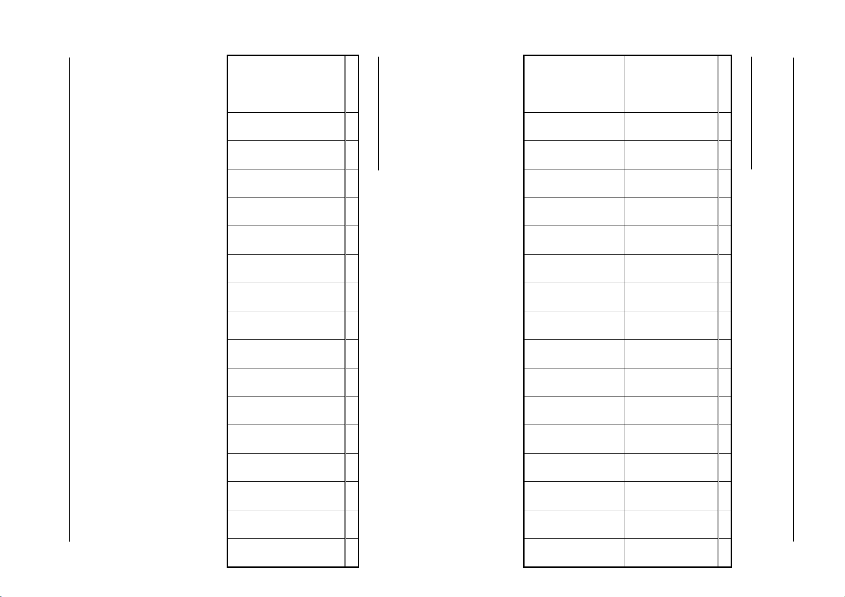
FC_STACK_LOCK_CLR (0x3A, write)
function
write
“1”
function
read
Bit 15 14 13 12 11 10 9 8 7 6 5 4 3 2 1 0
Bustec Production Ltd. Page 33
FC_STACK_LOCK_SET (0x38, read/write)
ProDAQ 3150 User Manual 3150UM-01
res
res
res
res
res
res
res
res
res
res
res
res
VXI FC_D Stack
clear MASTER bit
VXI FC_C Stack
clear MASTER bit
VXI FC_B Stack
clear MASTER bit
VXI FC_A Stack
clear MASTER bit
Power up or VXI reset condition: 0x0000
Stack FC_D: FC 8 and FC 7
Stack FC_C: FC 6 and FC 5
Stack FC_B: FC 4 and FC 3
Stack FC_A: FC 2 and FC 1
res
res
res
res
res
res
res
res
res
res
res
res
VXI FC_D Stack
REQUEST bit
VXI FC_C Stack
REQUEST bit
VXI FC_B Stack
REQUEST bit
VXI FC_A Stack
REQUEST bit
0
0
0
0
DSP FC_D Stack
MASTER bit
DSP FC_C Stack
MATER bit
DSP FC_B Stack
MASTER bit
DSP FC_A Stack
MASTER bit
LIST FC_D Stack
MASTER bit
LIST FC_C Stack
MASTER bit
LIST FC_B Stack
MASTER bit
LIST FC_A Stack
MASTER bit
VXI FC_D Stack
MASTER bit
VXI FC_C Stack
MASTRER bit
VXI FC_B Stack
MASTER bit
VXI FC_A Stack
MASTER bit
Artisan Technology Group - Quality Instrumentation ... Guaranteed | (888) 88-SOURCE | www.artisantg.com
Page 35
function
write
Bit 15 14 13 12 11 10 9 8 7 6 5 4 3 2 1 0
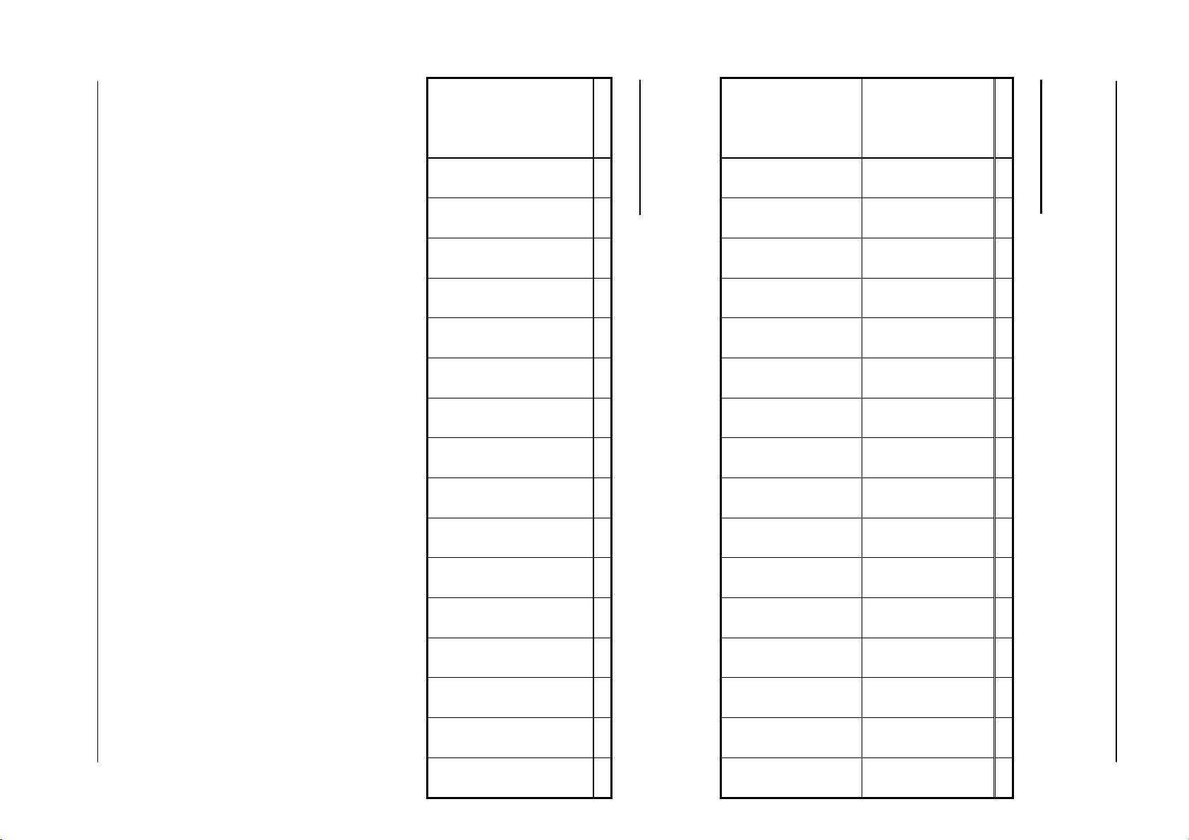
SOURCE_ARB_CLR (0x3E, write)
Power up or VXI reset condition: 0x0000
function
write
function
read
Bit 15 14 13 12 11 10 9 8 7 6 5 4 3 2 1 0
Page 34 Bustec Production Ltd.
SOURCE_ARB_SET (0x3C, read/write)
ProDAQ 3150 User Manual 3150UM-01
res
res
res
res
res
res
res
res
res
res
res
res
VXI JTAG clear
MASTER bit
VXI RAPID clear
MASTER bit
VXI FC_RESET clear
MATER bit
VXI VREF clear
MASTER bit
res
res
res
res
res
res
res
res
res
res
res
res
VXI JTAG
REQUEST bit
VXI RAPID
REQUEST bit
VXI FC_RESET
REQUEST bit
VXI VREF
REQUEST bit
0
0
0
VREF AAVAIL
DSP JTAG
MASTER bit
DSP RAPID
MATER bit
DSP FC_RESET
MASTER bit
DSP VREF
MASTER bit
LIST JTAG
MASTER bit
LIST RAPID
MASTER bit
LIST FC_RESET
MASTER bit
LIST VREF
MASTER bit
VXI JTAG
MASTER bit
VXI RAPID
MASTRER bit
VXI FC_RESET
MASTER bit
VXI VREF
MASTER bit
Artisan Technology Group - Quality Instrumentation ... Guaranteed | (888) 88-SOURCE | www.artisantg.com
Page 36
ProDAQ 3150 User Manual 3150UM-01
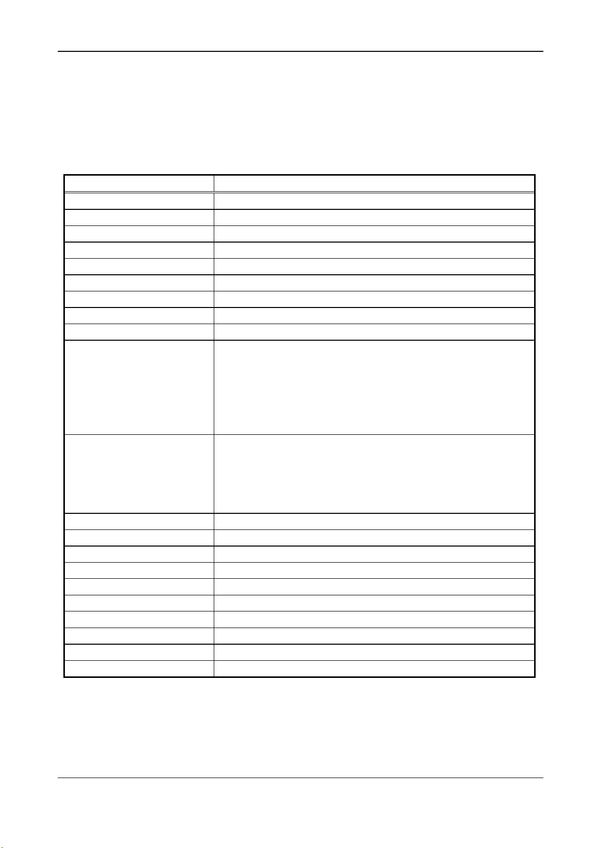
VXIbus Address Map
The following map describes the address space of the ProDAQ 3150 High-Performance Motherboard as
seen from the VXIbus. All addresses are shown relativ to the boards base address in the VXIbus A32
address space. The base address is set via the offset register in the VXIbus Configuration Registers.
A32 Offset Description
0x00000000 - 0x0003FFFF
0x00040000 - 0x0007FFFF
0x00080000 - 0x000BFFFF
0x000C0000 - 0x000FFFFF
0x00100000 - 0x0013FFFF
0x00140000 - 0x0017FFFF
0x00180000 - 0x001BFFFF
0x001C0000 - 0x001FFFFF
0x00200000 - 0x002FFFFF
0x00300000 - 0x0031FFFF
0x00320000 - 0x0032FFFF
0x00330000 - 0x003BFFFF
0x003C0000 - 0x003FFFFF
0x00400000 - 0x007FFFFF
0x00800000 - 0x00FFFFFF
0x02000000 - 0x02FFFFFF
0x03000000 - 0x03FFFFFF
0x08000000 - 0x0BFFFFFF
0x0C000000 - 0x0CFFFFFF
All addresses not explicitly specified are reserved for future use.
Function Card 1
Function Card 2
Function Card 3
Function Card 4
Function Card 5
Function Card 6
Function Card 7
Function Card 8
<not used>
Trigger Interface
0x00300000 - Trigger status register (32 bit word) with update
0x00300004 - Trigger rapid connect interface (32 bit word)
0x00300008 - Trigger status register without update
(e.g. IRQ response)
Voltage Reference Interface
0x00320000 - Voltage Reference (R/W MB buffer)
0x00320004 - Voltage Reference ID (read only)
0x00320008 - Voltage Reference Module Access
<not used>
broadcast to all FCs
List Processor Memory (SRAM, Flash) restricted access (4MB)
Optional DSP Memory (SRAM, Flash) restricted access (8MB)
Memory Bank 1 (16MB version)
Memory Bank 2 (16MB version)
Memory Bank 1 (64MB version)
Memory Bank 2 (64MB version)
Bustec Production Ltd. Page 35
Artisan Technology Group - Quality Instrumentation ... Guaranteed | (888) 88-SOURCE | www.artisantg.com
Page 37

ProDAQ 3150 User Manual 3150UM-01
Function Card Access
The function cards fitted into the ProDAQ 3150 High-Performance Motherboard can be accessed through
their address spaces in the boards address space. The function card address space (registers, memory,
etc.) is organized in 16-bit words. Using different mapping for the VXIbus access types, the function cards
can be accessed seperately, combined or all at once.
Single Function Card Access
When accessing a single function card, the VXIbus data cycles are mapped as:
D16 Single read FC Single Word Transfer Read
D16 Single write FC Single Word Transfer Write
D16 BLT read FC Block Transfer Read
D16 BLT write FC Block Transfer Write
D32 Single read FC Block Transfer Read (two 16-bit words)
D32 Single write FC Block Transfer Write (two 16-bit words)
D32 BLT read FC Block Transfer Read (n x two 16-bit words)
D32 BLT write FC Block Transfer Write (n x two 16-bit words)
Note: The 32-bit to two 16-bit word transfer order depends on the VME_ORDER bit in the Util register.
Multiple Function Card Access
By selecting functions cards in the FCMASK register, multiple function cards can be accessed
simultaneously. In this mode, VXIbus D32 data cycles are mapped as
D32 Single read 2 FC Single Word Transfer Read
D32 BLT read 2 FC Block Transfer Read
D32 Single write 2 FC Single Word Transfer Write
D32 BLT write 2 FC Block Transfer Write
In this mode, the lower 16-bit part of a D32 cycle will access one function card on stack A or C (function
cards 1, 2, 5, 6) while the upper 16-bit part will access one function card on stack B or D (function cards 3, 4,
7, 8). Write cycles may access all combination of cards simultaneously, while read cycles may only access
exactly two function cards (FC1 or FC2 or FC5 or FC6 AND FC3 or FC4 or FC7 or FC8).
Page 36 Bustec Production Ltd.
Artisan Technology Group - Quality Instrumentation ... Guaranteed | (888) 88-SOURCE | www.artisantg.com
Page 38
ProDAQ 3150 User Manual 3150UM-01
Broadcast Write access
A broadcast write will transfer the same data to all function cards simultaneously. This can be used for
example to start/stop all function cards at the same time. A broadcast write can be done by writing to the
defined address range in the motherboard address space (see VXIbus Address Map). VXIbus cylces are
mapped as:
D16 Single write FC-card Single Word Transfer Write
D16 BLT write FC-card Block Transfer Write
D32 Single write FC-card Block Transfer Write (two 16-bit words) *
D32 BLT write FC-card Block Transfer Write (n x two 16-bit words) *
Function cards accessed can be selected using the FCMASK register (bit 7 to bit 0). The 32-bit to two 16-bit
word transfer order depends on the VME_ORDER bit (Util register).
Internal Resources
Trigger status register with update (32 bit word)
Holds the actual level of the Trigger lines.
Trigger status register without update (32 bit word read only)
An interrupt request from the trigger matrix updates the register to allow the application program to
determine the interrupting source.
The register has the following bit assignment:
Bit 31 30 29 28 27 26 25 24
Name “1” “1” TMO 2 TMO 1 TMO 0 “1” ECLtrig 1 ECLtrig 0
Bit 23 22 21 20 19 18 17 16
Name TTLtrig 7 TTLtrig 6 TTLtrig 5 TTLtrig 4 TTLtrig 3 TTLtrig 2 TTLtrig 1 TTLtrig 0
Bit 15 14 13 12 11 10 9 8
Name FCtrgOut 7 FCtrgOut 6 FCtrgOut 5 FCtrgOut 4 FCtrgOut 3 FCtrgOut 2 FCtrgOut 1 FCtrgOut 0
Bit
Name FCtrgIn 7 FCtrgIn 6 FCtrgIn 5 FCtrgIn 4 FCtrgIn 3 FCtrgIn 2 FCtrgIn 1 FCtrgIn 0
7 6 5 4 3 2 1 0
TMO 0 … 2 Status of the trigger line from the communication registers to the trigger matrix
(actual level; “0” : active; “1” : not active)
ECLtrig 0 ...1 Status of the VXIbus ECL trigger lines
Bustec Production Ltd. Page 37
Artisan Technology Group - Quality Instrumentation ... Guaranteed | (888) 88-SOURCE | www.artisantg.com
Page 39

ProDAQ 3150 User Manual 3150UM-01
TTLtrig 0...7 Status of the VXIbus TTL trigger lines
FCtrgOut 0...7 Status of the function card output trigger lines
FCtrgIn 0...7 Status of the function card input trigger lines
Page 38 Bustec Production Ltd.
Artisan Technology Group - Quality Instrumentation ... Guaranteed | (888) 88-SOURCE | www.artisantg.com
Page 40
ProDAQ 3150 User Manual 3150UM-01
IBus Interface
FLASH
SRAM
Local
Chapter 6
The ProDAQ 3220 DSP Plug-in Module
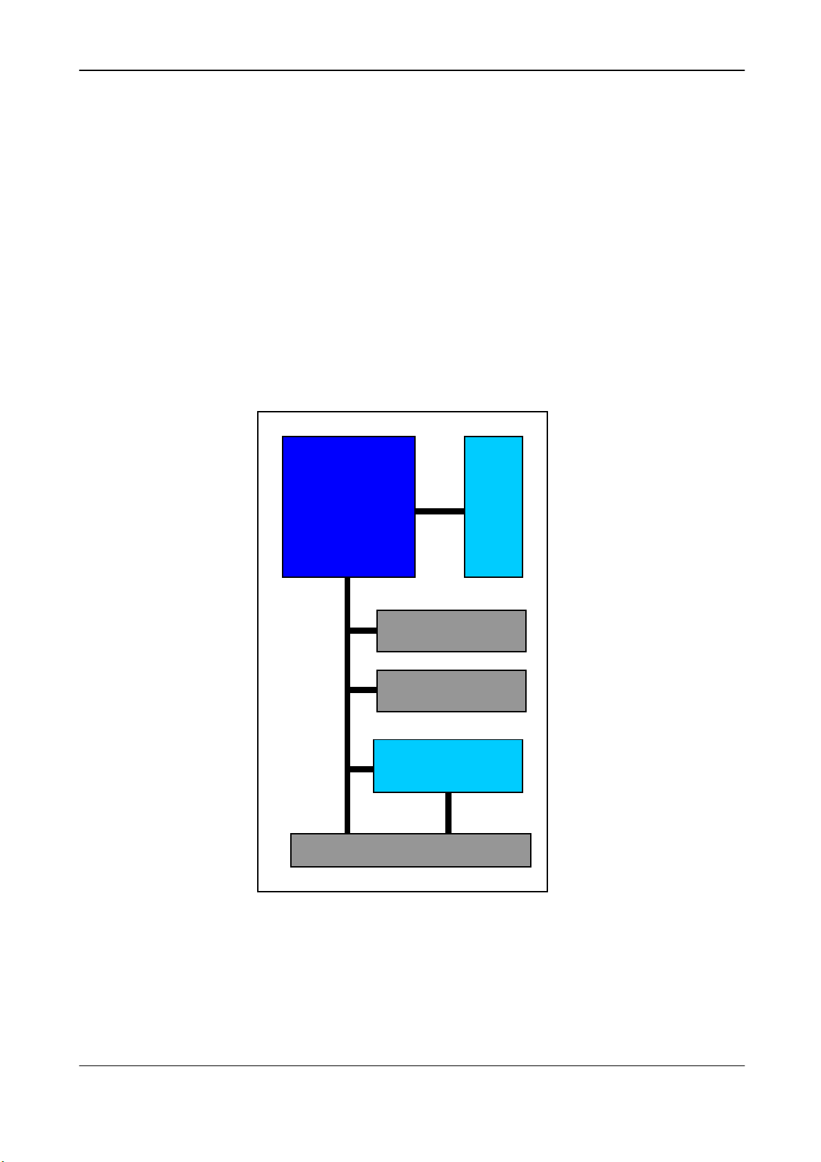
The ProDAQ DSP Plug-in Module adds a fully user-programmable DSP to the ProDAQ 3150 motherboard.
Overview
The ProDAQ 3220 DSP Plug-in module consists of a SHARC 21060 DSP with 512 KWord local SRAM and 4
MB local FLASH. It has two interfaces, one for the internal bus on the motherboard (iBus) amd one for the
VXIbus local bus. The interface for the iBus also implements a set of communication registers.
SHARC
Communication
Bus
Inter-
face
Register
The communication registers provide mailbox registers for the communication with the on-board processor or
a host and also registers for motherboard status and motherboard resources.
Bustec Production Ltd. Page 39
Figure 7 - DSP Plug-in Module Block Diagram
Artisan Technology Group - Quality Instrumentation ... Guaranteed | (888) 88-SOURCE | www.artisantg.com
Page 41

ProDAQ 3150 User Manual 3150UM-01
Programming Information
Address Map
Internal
Address Start
0x0040 0000 0x0043 FFFF 48 bit SRAM (256K x 48)
Internal
Address End
Data
Width
Description
0x0080 0000 0x0087 FFFF 8 bit
0x00C0 0000 0x00FF FFFF 16 bit
0x0100 0000 0x013F FFFF 16 bit
0x0140 0000 0xFFFF FFFF 32 bit
All addresses not explicitly specified are reserved for future use.
512K x 8 Flash Memory
(SHARC: Data [23:16])
Communication registers
(SHARC: Data[31:16] are used)
Local interface space
(SHARC: Data[31:16] are used)
Internal Bus
(SHARC: Data[47:16])
Page 40 Bustec Production Ltd.
Artisan Technology Group - Quality Instrumentation ... Guaranteed | (888) 88-SOURCE | www.artisantg.com
Page 42

ProDAQ 3150 User Manual 3150UM-01
Communication Registers (base address: 0x00C0 0000)
Address Mnemonic DSP
RW
0x00C0 0000 MB_Status R mailbox status register
0x00C0 0002 MB_VXI RW mailbox to and from VXI
0x00C0 0004 MB_DSP / MB_LIST RW mailbox to and from DSP / to and from LIST
0x00C0 0006 FC_AVAIL_RESET RW* reset control of FC-cards and status of FC_AVAIL bits
0x00C0 0008 SOURCE_ARB_SET RW software board arbitration register
0x00C0 000A SOURCE_ARB_CLR W software board arbitration register
0x00C0 000C IQ-JTAG RW* JTAG interface for switch matrix loading
0x00C0 000E TRG_RAPID W trigger rapid write interface
0x00C0 000F reserved reserved
0x00C0 0010 VREF_BUF RW* VREF buffer
0x00C0 0012 VREF_IDENT R VREF identifier
0x00C0 0014 VREF_ACCESS RW* VREF access
0x00C0 0016 reserved reserved
0x00C0 0018 TRIG_IN_EN_IRQ Trigger (LIST/DSP) IRQ2 Enable register
0x00C0 001A TRIG_OUT Trigger SET and status register
0x00C0 001B reserved reserved
0x00C0 001C reserved reserved
0x00C0 001D reserved reserved
0x00C0 001E reserved reserved
0x00C0 001F reserved reserved
0x00C0 0020 MODE R MODE register : DSP reset/run
0x00C0 0021 FC_MASK_BROAD R FC_MASK_BROAD register broadcast (Mode 7)
0x00C0 0022 FC_STACK_LOCK_
SET
0x00C0 0023 FC_STACK_LOCK_
CLR
0x00C0 0024 FC_DMA R FC_DMA register
0x00C0 0025 FC_STATUS R FC_STATUS register
RW Software FC-Card Stack arbitration register (Set Request)
W Software FC-Card Stack arbitration register (Release)
Function
(TM2..0,FC_TRIG_IN0..7)
RW* : write only possible if SHARC is MASTER of destination (defined in SOURCE_ARB_SET)
Bustec Production Ltd. Page 41
Artisan Technology Group - Quality Instrumentation ... Guaranteed | (888) 88-SOURCE | www.artisantg.com
Page 43

ProDAQ 3150 User Manual 3150UM-01
MB_STATUS (0x00C0 0000, read)
Bit 15 14 13 12 11 10 9 8 7 6 5 4 3 2 1 0
Function 0 0 0 0 0 0
0 0
0 0
sLPtoDSP
sVXItoDSP
sLPtoVXI signals message in LP to VXI mailbox register
sDSPtoVXI signals message in DSP to VXI mailbox register
sVXItoLP signals message in VXI to LP mailbox register
sDSPtoLP signals message in DSP to VXI mailbox register
sVXItoDSP signals message in VXI to DSP mailbox register
sLPtoDSP signals message in LP to DSP mailbox register
MB_VXI (0x00C0 0002, read/write)
The MAIILBOX register consists of two 16-bit registers:
MB_VXI_TO_DSP (read) and
MB_DSP_TO_VXI (write)
A write to this mailbox register sets a bit in the MB_STATUS register and causes (if enabled) an interrupt to
the destination, which is cleared after the destination processor has read the message register.
sVXItoLP
sDSPtoLP
sDSPtoVXI
MB_DSP (0x00C0 0004, read/write)
The MAIILBOX register set consists of two 16-bit registers:
MB_LP_TO_DSP (read) and
MB_DSP_TO_LP (write)
A write to this mailbox register sets a bit in the MB_STATUS register and causes (if enabled) an interrupt to
the destination, which is cleared after the destination processor has read the message register.
sLPtoVXI
Page 42 Bustec Production Ltd.
Artisan Technology Group - Quality Instrumentation ... Guaranteed | (888) 88-SOURCE | www.artisantg.com
Page 44

ProDAQ 3150 User Manual 3150UM-01
FC_AVAIL_RESET (0x00C0 0006, read/write)
Bit 15 14 13 12 11 10 9 8 7 6 5 4 3 2 1 0
Initial 0 0 0 0 0 0 0 0
read
function
FC8 AVAIL
FC7 AVAIL
FC6 AVAIL
FC5 AVAIL
FC4 AVAIL
FC3 AVAIL
FC2 AVAIL
FC1 AVAIL
FC 8
FC 7
FC 6
FC 5
FC 4
FC 3
FC 2
ENABLE (NOT RESET)
ENABLE (NOT RESET)
ENABLE (NOT RESET)
ENABLE (NOT RESET)
ENABLE (NOT RESET)
ENABLE (NOT RESET)
ENABLE (NOT RESET)
FC 1
ENABLE (NOT RESET)
write
res
res
res
res
res
res
res
function
res
FC 8
FC 7
FC 6
FC 5
ENABLE (NOT RESET)
ENABLE (NOT RESET)
ENABLE (NOT RESET)
ENABLE (NOT RESET)
ENABLE (NOT RESET)
FC1 ... FC8 AVAIL signals availability of the corresponding front end card
read:
ENABLE FC1 ... FC8 reflects the ENABLE/RESET status of the corresponding front end card
write:
ENABLE FC1 ... FC8 drive directly the reset lines to the function card located at the specific
position. To enable the function cards a 1 has to be written.
FC 4
FC 3
FC 2
FC 1
ENABLE (NOT RESET)
ENABLE (NOT RESET)
ENABLE (NOT RESET)
Bustec Production Ltd. Page 43
Artisan Technology Group - Quality Instrumentation ... Guaranteed | (888) 88-SOURCE | www.artisantg.com
Page 45
function
write
Bit 15 14 13 12 11 10 9 8 7 6 5 4 3 2 1 0
SOURCE_ARB_CLR (0x00C0 000A, write)
Power up or VXI reset condition: 0x0000
function
write
function
read
Bit 15 14 13 12 11 10 9 8 7 6 5 4 3 2 1 0
Page 44 Bustec Production Ltd.
SOURCE_ARB_SET (0x00C0 0008, read/write)
ProDAQ 3150 User Manual 3150UM-01
res
res
res
res
res
res
res
res
LIST JTAG clear
MASTER bit
LIST RAPID clear
MASTER bit
LIST FC_RESET clear
MATER bit
LIST VREF clear
MASTER bit
res
res
res
res
res
res
res
res
res
res
res
res
LIST JTAG
REQUEST bit
LIST RAPID
REQUEST bit
LIST FC_RESET
REQUEST bit
LIST VREF
REQUEST bit
res
res
res
res
0
0
0
VREF AVAIL
DSP JTAG
MASTER bit
DSP RAPID
MASTER bit
DSP FC_RESET
MASTER bit
DSP VREF
MASTER bit
LIST JTAG
MASTER bit
LIST RAPID
MASTER bit
LIST FC_RESET
MASTER bit
LIST VREF
MASTER bit
VXI JTAG
MASTER bit
VXI RAPID
MASTRER bit
VXI FC_RESET
MASTER bit
VXI VREF
MASTER bit
Artisan Technology Group - Quality Instrumentation ... Guaranteed | (888) 88-SOURCE | www.artisantg.com
Page 46
ProDAQ 3150 User Manual 3150UM-01
TMO
TMO
TMO
TRIG_IN_EN_IRQ (0x00C0 0018, read/write)
Bit 15 14 13 12 11 10 9 8 7 6 5 4 3 2 1 0
Operation RW RW RW RW RW RW RW RW RW RW RW RW RW RW RW RW
Initial 0 0 0 0 0 0 0 0 0 0 0 0 0 0 0 0
Name
VXITI 7 VXITI 6 VXITI 5 VXITI 4 VXITI 3 VXITI 2 VXITI 1 VXITI 0 FCTO 7 FCTO 6 FCTO 5 FCTO 4 FCTO 3 FCTO 2 FCTO 1 FCTO
FCTO 0 .. 7 Selects the FC trigger signals, which will generate a trigger interrupt for the DSP
(IRQ2)
VXITI 0 .. 7 Selects VXI trigger Signals, which will generate a trigger interrupt for the DSP
(IRQ2)
A write operation with a one to the appropriated bit enables the trigger generation.
In case of a read the bits which have been enabled and have caused an interrupt are active.
0
The bits which have caused an interrupt have to be cleared by disabling the appropriated bit.
TRIG_OUT (0x00C0 001A, read/write)
Bit 15 14 13 12 11 10 9 8 7 6 5 4 3 2 1 0
Operation RW RW RW RW RW RW RW RW RW RW RW RW RW RW RW RW
Initial 0 0 0 0 0 0 0 0 0 0 0 0 0 0 0 0
Name
LIST_FLAG2
_IRQ2
FL2 FL1 FL0
2
1
FCTI 7 FCTI 6 FCTI 5 FCTI 4 FCTI 3 FCTI 2 FCTI 1 FCTI
0
Read:
FCTI 0 … 7 Status of the Function card trigger input (actual level; “0” : active; “1” : not active)
TMO 0 … 2 Status of the trigger line from the communication registers to the trigger matrix
(actual level; “0” : active; “1” : not active)
FL0 … FL2 “0”
0
LIST_FLAG2_IRQ2 Status of the DSP IRQ2 LIST_FLAG2 flag
Write:
FCTI 0 … 7 “1” : set the Function card trigger input (set to low)
“0”: clear the Function card trigger input (tristate)
Bustec Production Ltd. Page 45
Artisan Technology Group - Quality Instrumentation ... Guaranteed | (888) 88-SOURCE | www.artisantg.com
Page 47

ProDAQ 3150 User Manual 3150UM-01
TMO 0 … 2 “1” : set the trigger line from the LIST communication register to the trigger matrix
(set to low)
“0” : clear the trigger line from the LIST communication register to the trigger matrix
(tristate)
FL0 … FL2 “1” : enables to use the the LP flag 0..2 signal to and sets the TMO 0 … 2 signal
LIST_FLAG2_IRQ2 “1” enables the DSP IRQ2 if the LIST FLAG2 is set (edge sensitive)
“0” disables and clears the DSP IRQ2 LIST_FLAG2 flag
MODE (0x00C0 0020, read/write)
Bit 15 14 13 12 11 10 9 8 7 6 5 4 3 2 1 0
Operation RO RO RO RO RO RO RO RO RO RO RO RO RO RO RO RW
Initial 0 0 0 0 0 0 0 0 0 0 0 0 0 0 0 0
Name
reserved
reserved
reserved
reserved
reserved
reserved
reserved
reserved
reserved
reserved
reserved
reserved
reserved
reserved
reserved
DSP_RESET : ored with the VXI DSP Reset
FC_MASK_BROAD (0x00C0 0021, read/write)
Used for broadcast write operations in Mode 7 (only LIST).
Bit 15 14 13 12 11 10 9 8 7 6 5 4 3 2 1 0
Operation RO RO RO RO RO RO RO RO RW RW RW RW RW RW RW RW
Initial 0 0 0 0 0 0 0 0 0 0 0 0 0 0 0 0
Name
FC 8
FC 7
FC 6
FC 5
FC 4
FC 3
FC 2
Bit 7 0 selected channels for write operation in Mode 7
DSP_RESET
FC 1
Page 46 Bustec Production Ltd.
Artisan Technology Group - Quality Instrumentation ... Guaranteed | (888) 88-SOURCE | www.artisantg.com
Page 48
function
write
“1”
Bit 15 14 13 12 11 10 9 8 7 6 5 4 3 2 1 0
FC_STACK_LOCK_CLR (0x00C00023; write)
Stack FC_B: FC 4 and FC 3
Stack FC_A: FC 2 and FC 1
Stack FC_D: FC 8 and FC 7
Stack FC_C: FC 6 and FC 5
Power up or VXI reset condition: 0x0000
function
write
“1”
function
read
Bit 15 14 13 12 11 10 9 8 7 6 5 4 3 2 1 0
Bustec Production Ltd. Page 47
FC_STACK_LOCK_SET (0x00C00022; read/write)
ProDAQ 3150 User Manual 3150UM-01
res
res
res
res
DSP FC_D Stack
clear MASTER bit
DSP FC_C Stack
clear MASTER bit
DSP FC_B Stack
clear MASTER bit
DSP FC_A Stack
clear MASTER bit
res
res
res
res
res
res
res
res
res
res
res
res
DSP FC_D Stack
REQUEST bit
DSP FC_C Stack
REQUEST bit
DSP FC_B Stack
REQUEST bit
DSP FC_A Stack
REQUEST bit
res
res
res
res
res
res
res
res
0
0
0
0
DSP FC_D Stack
MASTER bit
DSP FC_C Stack
MATER bit
DSP FC_B Stack
MASTER bit
DSP FC_A Stack
MASTER bit
LIST FC_D Stack
MASTER bit
LIST FC_C Stack
MASTER bit
LIST FC_B Stack
MASTER bit
LIST FC_A Stack
MASTER bit
VXI FC_D Stack
MASTER bit
VXI FC_C Stack
MASTRER bit
VXI FC_B Stack
MASTER bit
VXI FC_A Stack
MASTER bit
Artisan Technology Group - Quality Instrumentation ... Guaranteed | (888) 88-SOURCE | www.artisantg.com
Page 49

ProDAQ 3150 User Manual 3150UM-01
FC_STATUS (0x00C00025; read)
Bit 15 14 13 12 11 10 9 8 7 6 5 4 3 2 1 0
Function
0 0 0 0 0 0
DSP
PDB7
PDB6
PDB7
PDB6
DRAM Bank 2
DRAM Bank 2
NOT_DEF_CMD
DRAM Bank 1
FC_D_ERR
DRAM Bank 1
DSP LP reads a “0”; DSP reads a “1”
NOT_DEF_CMD indicates a not valid access on internal bus; cleared after Power Up
or VXI Reset
PDB7 DRAM Bank 2 memory ID bit 7 Bank2 (lower 72-pin SO-DIMM)
PDB6 DRAM Bank 2 memory ID bit 6 Bank2 (lower 72-pin SO-DIMM)
PDB7 DRAM Bank 1 memory ID bit 7 Bank1 (lower 72-pin SO-DIMM)
PDB6 DRAM Bank 1 memory ID bit 6 Bank1 (lower 72-pin SO-DIMM)
FC_D_ERR reflects the hardware signal FC_ERR of STACK FCD (FC7,FC8)
FC_C_ERR reflects the hardware signal FC_ERR of STACK FCC (FC5,FC6)
FC_B_ERR reflects the hardware signal FC_ERR of STACK FCB (FC3,FC4)
FC_A_ERR reflects the hardware signal FC_ERR of STACK FCA (FC1,FC2)
FC_B_ERR
FC_C_ERR
FC_A_ERR
Page 48 Bustec Production Ltd.
Artisan Technology Group - Quality Instrumentation ... Guaranteed | (888) 88-SOURCE | www.artisantg.com
Page 50

ProDAQ 3150 User Manual 3150UM-01
IBUS cycles (FC-SHARC-DRAM)
Sharc External Address commands
A31 A30 A29 A28 A27 A26 A25 A24
MODE
Bit M2
M2 M1 M0 Selected Mode
0 0 0 reserved
0 0 1 MODE 1: SHARC single read or write Cycle from or to FC-card
0 1 0 reserved
0 1 1 MODE 3: SHARC single read or write Cycle from or to DRAM
1 0 0 reserved
1 0 1 reserved
1 1 0 reserved
1 1 1 reserved
MODE 1 (SHARC single read or write Cycle)
A31 A30 A29
MODE
Bit M1
MODE
Bit M0
A28 A27 A26 A25 A24
depends
on MODE
depends
on MODE
depends
on MODE
depends
on MODE
depends
on MODE
0 0 1
0 0 1
0 0 1
0 0 1
0 0 1
0 0 1
0 0 1
- A23-A16 used as FC-card select lines
- write cycle to all FC-cards possible
D[15:0] assign to FCa, FCc
D[31:16] assign to FCb, FCd
- read cycle only from one or two FC-cards
FCa, FCc assign to D[15:0] ; use only one of the 4 FC-cards (FC1,2,5,6)
FCb, FCd assign to D[31:16] ; use only one of the 4 FC-cards (FC3,4,7,8)
0 0 0 FC
RD
0 0 1 FC
RD
0 1 0 x x FC-card AS disconnect cycle (clr AS)
0 1 1 x x Reserve
1 0 0 x x FC-card „normal“ Read/Write DS cycle
1 0 1 x x FC-card „pipe“ Read DS cycle
1 1 0 x x FC-card Read Latch cycle
x FC-card AS cycle (only write)
x FC-card AS cycle and hold AS (only write)
(read FC-Latch and then start DS cycle)
(read FC-Latch)
Bustec Production Ltd. Page 49
Artisan Technology Group - Quality Instrumentation ... Guaranteed | (888) 88-SOURCE | www.artisantg.com
Page 51

ProDAQ 3150 User Manual 3150UM-01
selected FC-card use FC-card AS data
from
IBUS Data path
FC 1 (A16=1) [15:0] [15:0]
FC 2 (A17=1) [15:0] [15:0]
FC 3 (A18=1) [31:16] [31:16]
FC 4 (A19=1) [31:16] [31:16]
FC 5 (A20=1) [15:0] [15:0]
FC 6 (A21=1) [15:0] [15:0]
FC 7 (A22=1) [31:16] [31:16]
FC 8 (A23=1) [31:16] [31:16]
use FC DS data
from/to
IBUS Data path
MODE 3 (SHARC single read or write Cycle)
A31 A30 A29
A28 A27 A26 A25 A24
0 1 1
0 1 1
A PAGE-bit will be set during a DRAM read cycle if addr. Bit 25 is 1. If this bit is SET, then the DRAM bank
gets locked and access to the DRAM is faster and locked.
You can CLEAR this PAGE bit during a DRAM read cycle if addr Bit 26 is 1.
Example:
#define DRAM_ADDR00_ENPAGE 0x62000000
#define DRAM_ADDR00_DISPAGE 0x64000000
FC_MODE7_LOOP:
R2=DM (DRAM_ADDR00_ENPAGE);
DM (FC_AS_WRITE_HOLD,I1)=R1;
R2=DM (FC_DMA_MODE7,I5);
R2=DM (FC_DMA_MODE7+1,I5);
R2=DM (FC_DMA_MODE7+2,I5);
R2=DM (FC_DMA_MODE7+3,I5);
DM (FC_AS_CLEAR_HOLD,I1)=R1;
R2=DM (DRAM_ADDR00_DISPAGE);
JUMP (PC,Delay1)
x x CLR_
PAGE
x x CLR_
PAGE
SET_
PAGE
SET_
PAGE
0 DRAM Bank 1
1 DRAM Bank 2
Page 50 Bustec Production Ltd.
Artisan Technology Group - Quality Instrumentation ... Guaranteed | (888) 88-SOURCE | www.artisantg.com
Page 52
ProDAQ 3150 User Manual 3150UM-01
VXI Local Bus Interface
The VXI Local Bus interface of the DSP plug-in module can be used in two different ways, either by routing
the SHARC link interface lines to the VXI local bus lines or by addressing the lines of the VXI local bus
directly via a register.
DSP VXI Local Bus interface registers (base address: 0x0100 0000)
Address Mnemonic DSP
RW
0x0100 0000 LOC_CONTROL RW LOCAL Bus interface Control register
0x0100 0002 LOC_P2A_OUT RW Output register to set VXI Local bus P2A lines
0x0100 0003 LOC_P2C_OUT RW Output register to set VXI Local bus P2C lines
0x0100 0004 LOC_P2A_IN R Status of VXI Local bus P2A lines
0x0100 0005 LOC_P2C_IN R Status of VXI Local bus P2C lines
Note: For accessing these registers the SHARC WAIT register has to be set to 0x2004EAA5
Function
Bustec Production Ltd. Page 51
Artisan Technology Group - Quality Instrumentation ... Guaranteed | (888) 88-SOURCE | www.artisantg.com
Page 53

ProDAQ 3150 User Manual 3150UM-01
LOC_CONTROL (0x0100 0000, read/write)
Bit 15 14 13 12 11 10 9 8 7 6 5 4 3 2 1 0
Operation RW RW RW RW RW RW RW RW RW RW RW RW RW RW RW RW
Initial 0 0 0 0 0 0 0 0 0 0 0 0 0 0 0 0
Name
ENABLE_LOC_P2C
ENABLE_LOC_P2A
reserved
reserved
reserved
reserved
ENABLE_P2C_ OUT_REG
ENABLE_P2A_ OUT_REG
TRANSMIT_ LINK3
ENABLE _LINK3
TRANSMIT_ LINK2
ENABLE _LINK2
TRANSMIT_ LINK1
ENABLE _LINK1
TRANSMIT_ LINK0
ENABLE _LINK0
ENABLE_LOC_P2C enables FET-driver for VXI LBUSC0..11 lines on the HPM
ENABLE_LOC_P2A enables FET-driver for VXI LBUSA0..11 lines on the HPM
ENABLE_P2C_ OUT_REG enables LOC_P2C_OUT register outputs to lines VXI LBUSC0..11
ENABLE_P2A_ OUT_REG enables LOC_P2A_OUT register outputs to lines VXI LBUSA0..11
TRANSMIT_ LINK3 “1”: SHARC Link3 transmit data; “0”: SHARC Link3 receive data
ENABLE _LINK3 enables SHARC Link3 in/outputs to lines VXI LBUSC6..11
TRANSMIT_ LINK2 “1”: SHARC Link2 transmit data; “0”: SHARC Link2 receive data
ENABLE _LINK2 enables SHARC Link2 in/outputs to lines VXI LBUSC0..5
TRANSMIT_ LINK1 “1”: SHARC Link1 transmit data; “0”: SHARC Link1 receive data
ENABLE _LINK1 enables SHARC Link1 in/outputs to lines VXI LBUSA6..11
TRANSMIT_ LINK0 “1”: SHARC Link0 transmit data; “0”: SHARC Link0 receive data
ENABLE _LINK0 enables SHARC Link0 in/outputs to lines VXI LBUSA0..5
Attention: Do not enable ENABLE_P2C_ OUT_REG and ENABLE_LINK3/2 at the same time.
Do not enable ENABLE_P2A_ OUT_REG and ENABLE_LINK1/0 at the same time.
Page 52 Bustec Production Ltd.
Artisan Technology Group - Quality Instrumentation ... Guaranteed | (888) 88-SOURCE | www.artisantg.com
Page 54
ProDAQ 3150 User Manual 3150UM-01
Pin assignment
Sharc Link 0 VXI Local bus P2 connector
L0ACK VXI LBUSA0 5A
L0CLK VXI LBUSA1 6A
L0DATA0 VXI LBUSA2 8A
L0DATA1 VXI LBUSA3 9A
L0DATA2 VXI LBUSA4 11A
L0DATA3 VXI LBUSA5 12A
Sharc Link 1 VXI Local bus P2 connector
L1ACK VXI LBUSA6 14A
L1CLK VXI LBUSA7 15A
L1DATA0 VXI LBUSA8 17A
L1DATA1 VXI LBUSA9 18A
L1DATA2 VXI LBUSA10 20A
L1DATA3 VXI LBUSA11 21A
Sharc Link 2 VXI Local bus P2 connector
L2ACK VXI LBUSC0 5C
L2CLK VXI LBUSC1 6C
L2DATA0 VXI LBUSC2 8C
L2DATA1 VXI LBUSC3 9C
L2DATA2 VXI LBUSC4 11C
L2DATA3 VXI LBUSC5 12C
Sharc Link 3 VXI Local bus P2 connector
L3ACK VXI LBUSC6 14C
L3CLK VXI LBUSC7 15C
L3DATA0 VXI LBUSC8 17C
L3DATA1 VXI LBUSC9 18C
L3DATA2 VXI LBUSC10 20C
L3DATA3 VXI LBUSC11 21C
Bustec Production Ltd. Page 53
Artisan Technology Group - Quality Instrumentation ... Guaranteed | (888) 88-SOURCE | www.artisantg.com
Page 55
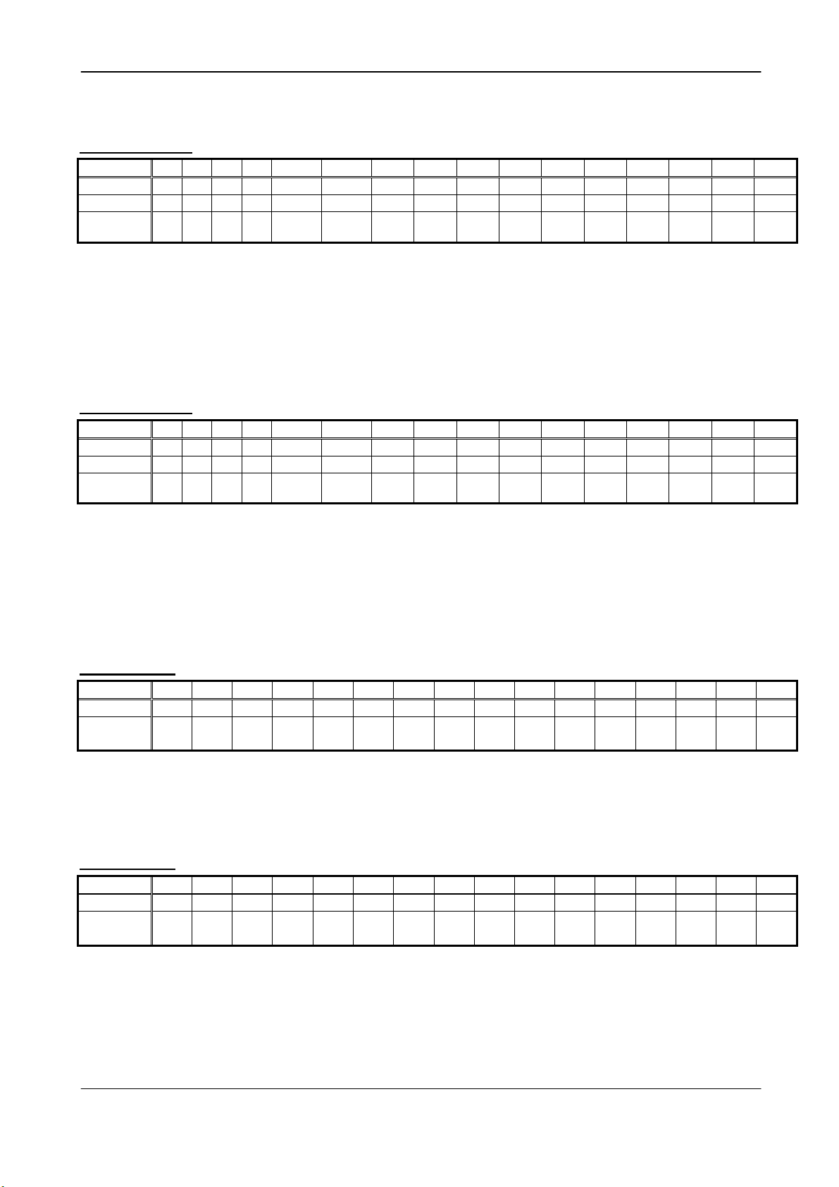
ProDAQ 3150 User Manual 3150UM-01
LOC_P2A_OUT (0x0100 0002, read/write)
Bit 15 14 13 12 11 10 9 8 7 6 5 4 3 2 1 0
Operation R R R R RW RW RW RW RW RW RW RW RW RW RW RW
Initial 0 0 0 0 0 0 0 0 0 0 0 0 0 0 0 0
Name “0” “0” “0” “0”
P2A_
OUT11
P2A_
OUT 10
P2A_
OUT 9
P2A_
OUT 8
P2A_
OUT 7
P2A_
OUT 6
P2A_
OUT 5
P2A_
OUT 4
P2A_
OUT 3
P2A_
OUT 2
P2A_
OUT 1
P2A_
OUT 0
P2A_OUT 0 … 11 “1” : sets the VXI Local bus signals LBUSA0..11
if P2A-FET driver is enabled and ENABLE_P2A_ OUT_REG is
enabled
(ENABLE_LOC_P2A = 1 and ENABLE_P2A_ OUT_REG = 1)
LOC_P2C_OUT (0x0100 0003, read/write)
Bit 15 14 13 12 11 10 9 8 7 6 5 4 3 2 1 0
Operation R R R R RW RW RW RW RW RW RW RW RW RW RW RW
Initial 0 0 0 0 0 0 0 0 0 0 0 0 0 0 0 0
Name “0” “0” “0” “0”
P2C_
OUT11
P2C_
OUT 10
P2C_
OUT 9
P2C_
OUT 8
P2C_
OUT 7
P2C_
OUT 6
P2C_
OUT 5
P2C_
OUT 4
P2C_
OUT 3
P2C_
OUT 2
P2C_
OUT 1
P2C_
OUT 0
P2C_OUT 0 … 11 “1” : sets the VXI Local bus signals LBUSC0..11
if P2C-FET driver is enabled and ENABLE_P2C_ OUT_REG is
enabled
(ENABLE_LOC_P2C = 1 and ENABLE_P2C_ OUT_REG = 1)
LOC_P2A_IN (0x0100 0004, read)
Bit 15 14 13 12 11 10 9 8 7 6 5 4 3 2 1 0
Operation R R R R R R R R R R R R R R R R
P2A_
P2A_
P2A_
P2A_
P2A_
P2A_
P2A_
P2A_
P2A_
P2A_
P2A_
Name “0” “0” “0” “0”
IN11
IN10
IN9
IN8
IN7
IN6
IN5
IN4
IN3
IN2
IN1
P2A_
IN0
P2A_IN 0 … 11 Status of the VXI Local bus signals LBUSA0..11 (if P2A-FET driver is
enabled)
LOC_P2C_IN (0x0100 0005, read)
Bit 15 14 13 12 11 10 9 8 7 6 5 4 3 2 1 0
Operation R R R R R R R R R R R R R R R R
P2C_
P2C_
P2C_
P2C_
P2C_
P2C_
P2C_
P2C_
P2C_
P2C_
P2C_
Name “0” “0” “0” “0”
IN11
IN10
IN9
IN8
IN7
IN6
IN5
IN4
IN3
IN2
IN1
P2C_
IN0
P2C_IN 0 … 11 Status of the VXI Local bus signals LBUSC0..11 (if P2C-FET driver is enabled)
Page 54 Bustec Production Ltd.
Artisan Technology Group - Quality Instrumentation ... Guaranteed | (888) 88-SOURCE | www.artisantg.com
Page 56

Artisan Technology Group is your source for quality
new and certied-used/pre-owned equipment
• FAST SHIPPING AND
DELIVERY
• TENS OF THOUSANDS OF
IN-STOCK ITEMS
• EQUIPMENT DEMOS
• HUNDREDS OF
MANUFACTURERS
SUPPORTED
• LEASING/MONTHLY
RENTALS
• ITAR CERTIFIED
SECURE ASSET SOLUTIONS
SERVICE CENTER REPAIRS
Experienced engineers and technicians on staff
at our full-service, in-house repair center
Instra
Remotely inspect equipment before purchasing with
our interactive website at www.instraview.com
Contact us: (888) 88-SOURCE | [email protected] | www.artisantg.com
SM
REMOTE INSPECTION
View
WE BUY USED EQUIPMENT
Sell your excess, underutilized, and idle used equipment
We also offer credit for buy-backs and trade-ins
www.artisantg.com/WeBuyEquipment
LOOKING FOR MORE INFORMATION?
Visit us on the web at www.artisantg.com for more
information on price quotations, drivers, technical
specications, manuals, and documentation
 Loading...