

Burr-Brown Corporation OPA277, OPA4277, OPA2277 User Manual

1
2
3
4
Offset Trim
−In
+In
V−
8
7
6
5
Offset Trim
Pin 1
Indicator
OPA277AIDRM
DFN-8 4mm x 4mm
(top view)
V+
Output
Thermal Pad
on Bottom
(Connect to V−)
NC
O
OPA277
O
P
A
2
7
7
O
P
P
A
A
2
2
7
2
O
7
7
OPA4277
P
A
4
2
7
7
7
OPA2277
O
P
A
2
2
7
7
SBOS079A – MARCH 1999 – REVISED APRIL 2005
High Precision
OPERATIONAL AMPLIFIERS
OPA277
OPA2277
OPA4277
FEATURES
● ULTRA LOW OFFSET VOLTAGE: 10µV
● ULTRA LOW DRIFT: ±0.1µV/°C
● HIGH OPEN-LOOP GAIN: 134dB
● HIGH COMMON-MODE REJECTION: 140dB
● HIGH POWER SUPPLY REJECTION: 130dB
● LOW BIAS CURRENT: 1nA max
● WIDE SUPPLY RANGE: ±2V to ±18V
● LOW QUIESCENT CURRENT: 800µA/amplifier
● SINGLE, DUAL, AND QUAD VERSIONS
● REPLACES OP-07, OP-77, OP-177
APPLICATIONS
● TRANSDUCER AMPLIFIER
● BRIDGE AMPLIFIER
● TEMPERATURE MEASUREMENTS
● STRAIN GAGE AMPLIFIER
● PRECISION INTEGRATOR
● BATTERY POWERED INSTRUMENTS
● TEST EQUIPMENT
OPA277
Offset Trim
Out A
–In A
+In A
V–
1
–In
2
+In
3
V–
4
1
2
3
4
8-Pin DIP, SO-8
8-Pin DIP, SO-8
OPA2277
A
B
Offset Trim
8
V+
7
Output
6
NC
5
Out A
1
–In A
2
+In A
3
V+
4
+In B
5
–In B
6
Out B
V+
8
Out B
7
–In B
6
+In B
5
7
OPA4277
AD
BC
14-Pin DIP, SO-14
NC = No connection.
DESCRIPTION
The OPA277 series precision op amps replace the industry
standard OP-177. They offer improved noise, wider output
voltage swing, and are twice as fast with half the quiescent
current. Features include ultra low offset voltage and drift, low
bias current, high common-mode rejection, and high power
supply rejection. Single, dual, and quad versions have identical
specifications for maximum design flexibility.
OPA277 series op amps operate from ±2V to ±18V supplies with
excellent performance. Unlike most op amps which are specified
at only one supply voltage, the OPA277 series is specified for
real-world applications; a single limit applies over the ±5V to
±15V supply range. High performance is maintained as the
amplifiers swing to their specified limits. Because the initial offset
voltage (±20µV max) is so low, user adjustment is usually not
required. However, the single version (OPA277) provides external trim pins for special applications.
OPA277 op amps are easy to use and free from phase inversion
and overload problems found in some other op amps. They are
stable in unity gain and provide excellent dynamic behavior over
a wide range of load conditions. Dual and quad versions feature
completely independent circuitry for lowest crosstalk and freedom from interaction, even when overdriven or overloaded.
Single (OPA277) and dual (OPA2277) versions are available
in DIP-8, SO-8, and DFN-8 (4mm x 4mm) packages. The quad
(OPA4277) comes in DIP-14 and SO-14 surface-mount packages. All are fully specified from –40°C to +85°C and operate
from –55°C to +125°C.
Out D
14
–In D
13
+In D
12
V–
11
Out A
+In C
10
–In C
9
8
Out C
−In A
+In A
V−
1
2
3
4
OPA2277AIDRM
Pin 1
Indicator
DFN-8 4mm x 4mm
(top view)
8
Out B
7
V+
6
−In B
5
+In B
Thermal Pad
on Bottom
(Connect to V−)
All trademarks are the property of their respective owners.
PRODUCTION DATA information is current as of publication date.
Products conform to specifications per the terms of Texas Instruments
standard warranty. Production processing does not necessarily include
testing of all parameters.
Please be aware that an important notice concerning availability, standard warranty, and use in critical applications of
Texas Instruments semiconductor products and disclaimers thereto appears at the end of this data sheet.
Copyright © 1999-2005, Texas Instruments Incorporated
www.ti.com

ABSOLUTE MAXIMUM RATINGS
Supply Voltage .................................................................................... 36V
Input Voltage ..................................................... (V–) –0.7V to (V+) +0.7V
Output Short-Circuit
Operating Temperature .................................................. –55°C to +125°C
Storage Temperature ..................................................... –55°C to +125°C
Junction Temperature ...................................................................... 150°C
Lead Temperature (soldering, 10s)................................................. 300°C
ESD Rating (Human Body Model) .................................................. 2000V
NOTE: (1) Stresses above these rating may cause permanent damage.
Exposure to absolute maximum conditions for extended periods may degrade
device reliability. (2) Short-circuit to ground, one amplifier per package.
(2)
.............................................................. Continuous
(Machine Model) ........................................................... 100V
(1)
ELECTROSTATIC
DISCHARGE SENSITIVITY
This integrated circuit can be damaged by ESD. Texas Instruments recommends that all integrated circuits be handled with
appropriate precautions. Failure to observe proper handling
and installation procedures can cause damage.
ESD damage can range from subtle performance degradation
to complete device failure. Precision integrated circuits may be
more susceptible to damage because very small parametric
changes could cause the device not to meet its published
specifications.
PACKAGE/ORDERING INFORMATION
PRODUCT max,
Single
OPA277PA ±50 ±1 DIP-8
OPA277P ±20 ±0.15 DIP-8
OPA277UA ±50 ±1 SO-8 Surface Mount
OPA277U ±20 ±0.15 SO-8 Surface Mount
OPA277AIDRM ±100 ±1 DFN-8 (4mm x 4mm)
Dual
OPA2277PA ±50 ±1 DIP-8
OPA2277P ±25 ±0.25 DIP-8
OPA2277UA ±50 ±1 SO-8 Surface Mount
OPA2277U ±25 ±0.25 SO-8 Surface Mount
OPA2277AIDRM ±100 ±1 DFN-8 (4mm x 4mm)
Quad
OPA4277PA ±50 ±1 DIP-14
OPA4277UA ±50 ±1 SO-14 Surface Mount
NOTE: (1) For the most current package and ordering information, see the Package Option Addendum located at the end of this data sheet or visit the TI web site
at www.ti.com.
(1)
OFFSET OFFSET
VOLTAGE VOLTAGE DRIFT
µV max, µV/°C PACKAGE-LEAD
PIN DESCRIPTIONS
OPA277
–In
+In
Out A
–In A
+In A
1
2
3
4
V–
8-Pin DIP, SO-8
OPA2277
1
A
2
3
V–
4
8-Pin DIP, SO-8
Offset Trim
OPA2277AIDRM
Offset Trim
8
V+
7
Output
6
(1)
NC
5
Out A
1
–In A
2
+In A
3
V+
4
+In B
5
–In B
6
Out B
7
V+
8
Out B
7
B
–In B
6
+In B
5
OPA4277
14
AD
BC
14-Pin DIP, SO-14
13
12
11
10
Out D
–In D
+In D
V–
+In C
–In C
9
Out C
8
Offset Trim
NOTE: (1) NC = No connection.
Out A
−In A
+In A
1
Pin 1
2
Indicator
3
4
V−
DFN-8 4mm x 4mm
(top view)
OPA277AIDRM
1
Pin 1
2
−In
+In
V−
3
4
DFN-8 4mm x 4mm
Indicator
(top view)
8
7
6
5
8
7
6
5
Out B
V+
−In B
+In B
Offset Trim
V+
Output
NC
Thermal Pad
on Bottom
(Connect to V−)
Thermal Pad
on Bottom
(Connect to V−)
2
www.ti.com
OPA277, OPA2277, OPA4277
SBOS079A

ELECTRICAL CHARACTERISTICS: VS = ±5V to VS = ±15V
At TA = +25°C, and RL = 2kΩ, unless otherwise noted.
Boldface limits apply over the specified temperature range, –40°C to +85°C.
OPA277P, U OPA2277PA, UA OPA277AIDRM,
OPA2277P, U OPA4277PA, UA OPA2277AIDRM
PARAMETER CONDITION MIN TYP
(1)
MAX MIN TYP
OFFSET VOLTAGE
Input Offset Voltage: V
OPA277P, U (high grade, single) ±10 ±20 µV
OS
OPA2277P, U (high grade, dual) ±10 ±25 µV
All PA, UA, Versions ±20 ±50 µV
AIDRM Versions ±35 ±100 µV
Input Offset Voltage Over Temperature
OPA277P, U (high grade, single) T
OPA2277P, U (high grade, dual) T
All PA, UA, Versions T
AIDRM Versions T
Input Offset Voltage Drift dV
OPA277P, U (high grade, single) T
/dT
OS
OPA2277P, U (high grade, dual) T
All PA, UA, AIDRM Versions T
= –40°C to +85°C
A
= –40°C to +85°C
A
= –40°C to +85°C
A
= –40°C to +85°C
A
= –40°C to +85°C
A
= –40°C to +85°C
A
= –40°C to +85°C
A
±
30 µV
±
50 µV
±
0.1
±
±
0.15 µV/°C
0.1
±
0.25 µV/°C
Input Offset Voltage: (all models)
vs Time 0.2 ✻✻µV/mo
vs Power Supply PSRR V
T
= –40°C to +85°C VS = ±2V to ±18V
A
Channel Separation (dual, quad) dc 0.1 ✻✻µV/V
= ±2V to ±18V ±0.3 ±0.5 ✻ ±1 ✻ ±1 µV/V
S
±
0.5
INPUT BIAS CURRENT
Input Bias Current I
T
= –40°C to +85°C
A
Input Offset Current I
T
= –40°C to +85°C
A
B
OS
±0.5 ±1 ✻ ±2.8 ±2.8 nA
±
2
±0.5 ±1 ✻ ±2.8 ±2.8 nA
±
2
NOISE
Input Voltage Noise, f = 0.1 to 10Hz 0.22 ✻✻µV
0.035 ✻✻µVrms
Input Voltage Noise Density, f = 10Hz e
f = 100Hz 8 ✻✻nV/√Hz
n
12 ✻✻nV/√Hz
f = 1kHz 8 ✻✻nV/√Hz
f = 10kHz 8 ✻✻nV/√Hz
Current Noise Density, f = 1kHz i
n
0.2 ✻✻pA/√Hz
INPUT VOLTAGE RANGE
Common-Mode Voltage Range V
Common-Mode Rejection CMRR V
T
= –40°C to +85°C VCM = (V–) +2V to (V+) –2V 128 115 115 dB
A
CM
= (V–) +2V to (V+) –2V 130 140 115 ✻ 115 ✻ dB
CM
(V–) +2 (V+) –2 ✻✻✻✻V
INPUT IMPEDANCE
Differential 100 || 3 ✻✻MΩ || pF
Common-Mode V
= (V–) +2V to (V+) –2V 250 || 3 ✻✻GΩ || pF
CM
OPEN-LOOP GAIN
Open-Loop Voltage Gain A
= –40°C to +85°CV
T
A
OL
VO = (V–)+0.5V to
(V+)–1.2V, R
V
(V+)–1.5V, R
(V+)–1.5V, R
= 10kΩ 140 ✻✻dB
L
= (V–)+1.5V to
O
= 2kΩ 126 134 ✻✻ ✻✻ dB
L
= (V–)+1.5V to
O
= 2kΩ 126 ✻✻dB
L
FREQUENCY RESPONSE
Gain-Bandwidth Product GBW 1 ✻✻MHz
Slew Rate SR 0.8 ✻✻V/µs
Settling Time, 0.1% V
0.01% V
Overload Recovery Time V
Total Harmonic Distortion + Noise THD+N 1kHz, G = 1, V
= ±15V, G = 1, 10V Step 14 ✻✻µs
S
= ±15V, G = 1, 10V Step 16 ✻✻µs
S
• G = V
IN
S
= 3.5Vrms 0.002 ✻✻%
O
3 ✻✻µs
✻ Specifications same as OPA277P, U.
NOTE: (1) V
= ±15V.
S
OPA277PA, UA
(1)
±
0.15
±
(1)
0.15
MAX UNITS
±
165 µV
±
1 µV/°C
±
1 µV/V
±
4nA
±
4nA
MAX MIN TYP
±
100 µV
±
1
±
1
±
4
±
4
PP
OPA277, OPA2277, OPA4277
SBOS079A
www.ti.com
3

ELECTRICAL CHARACTERISTICS: VS = ±5V to VS = ±15V (CONT)
At TA = +25°C, and RL = 2kΩ, unless otherwise noted.
Boldface limits apply over the specified temperature range, –40°C to +85°C.
OPA277P, U OPA2277PA, UA OPA277AIDRM,
OPA2277P, U OPA4277PA, UA OPA2277AIDRM
PARAMETER CONDITION MIN TYP
(1)
MAX MIN TYP
OUTPUT
Voltage Output V
T
= –40°C to +85°C RL = 10kΩ (V–) +0.5 (V+) –1.2 ✻✻✻✻V
A
T
= –40°C to +85°C RL = 2kΩ (V–) +1.5 (V+) –1.5 ✻✻✻✻V
A
Short-Circuit Current I
Capacitive Load Drive C
O
SC
LOAD
RL = 10kΩ (V–) +0.5 (V+) –1.2 ✻✻✻✻V
R
= 2kΩ (V–) +1.5 (V+) –1.5 ✻✻✻✻V
L
±35 ✻✻mA
See Typical Curve ✻✻
POWER SUPPLY
Specified Voltage Range V
Operating Voltage Range ±2 ±18 ✻✻✻✻V
Quiescent Current (per amplifier) I
T
= –40°C to +85°C IO = 0
A
S
Q
IO = 0 ±790 ±825 ✻✻ ✻✻µA
±5 ±15 ✻✻✻✻V
±
900 ✻✻µA
TEMPERATURE RANGE
Specified Range –40 +85 ✻✻✻✻°C
Operating Range –55 +125 ✻✻✻✻°C
Storage Range –55 +125 ✻✻✻✻°C
Thermal Resistance
SO-8 Surface-Mount 150 ✻ °C/W
θ
JA
DIP-8 100 ✻ °C/W
DIP-14 80 ✻ °C/W
SO-14 Surface-Mount 100 ✻ °C/W
(2)
DFN-8
✻ Specifications same as OPA277P, U.
NOTES: (1) V
= ±15V.
S
(2) Thermal pad soldered to printed circuit board (PCB).
OPA277PA, UA
(1)
MAX MIN TYP
(1)
MAX UNITS
45 °C/W
4
www.ti.com
OPA277, OPA2277, OPA4277
SBOS079A
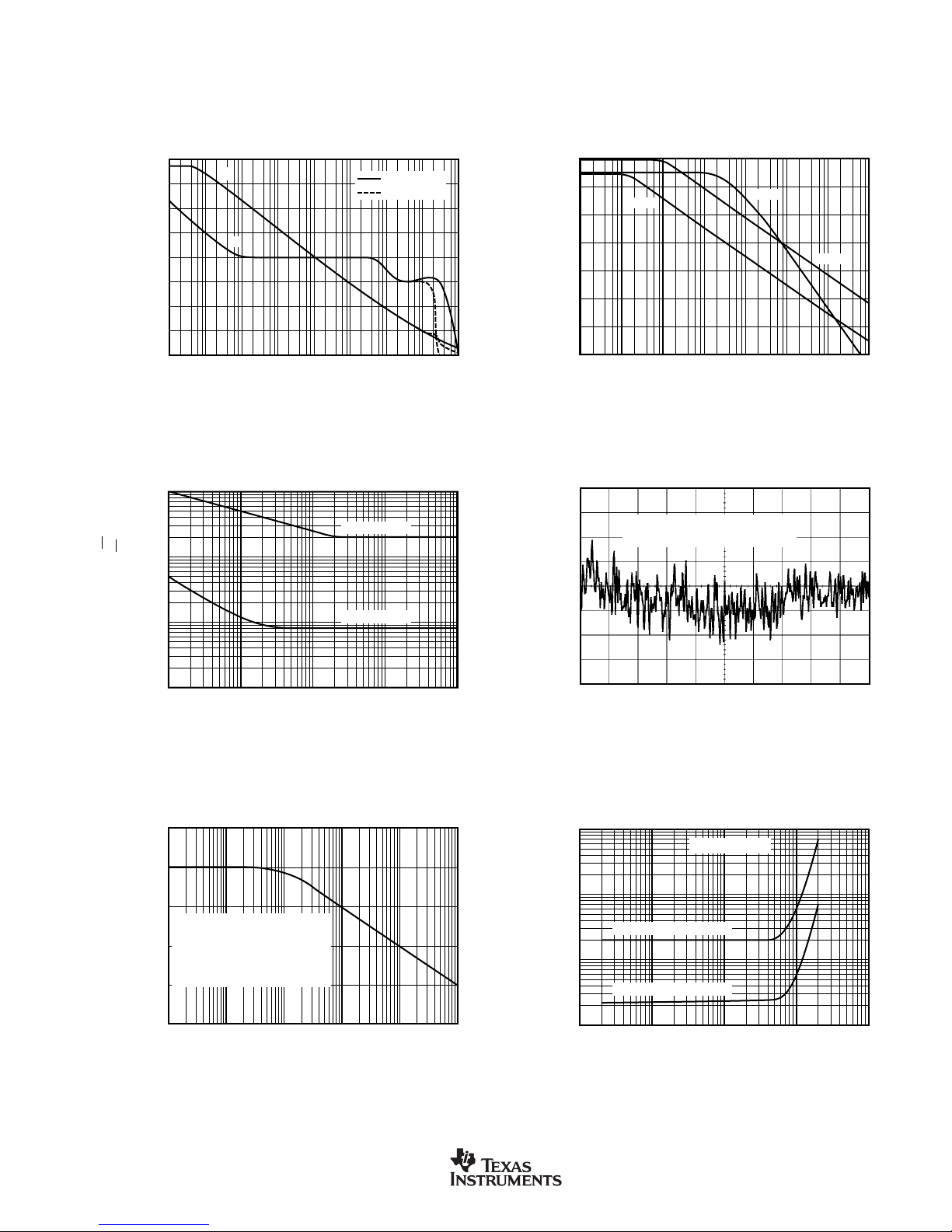
TYPICAL CHARACTERISTICS
10 100 1k 10k 100k
1
0.1
0.01
0.001
THD+Noise (%)
Frequency (Hz)
TOTAL HARMONIC DISTORTION + NOISE
vs FREQUENCY
V
OUT
= 3.5Vrms
G = 10, RL = 2kΩ, 10kΩ
G = 1, RL = 2kΩ, 10kΩ
0.1 1 10 100 1k 10k 100k 1M
140
120
100
80
60
40
20
0
PSR, CMR (dB)
Frequency (Hz)
POWER SUPPLY AND COMMON-MODE
REJECTION vs FREQUENCY
+PSR
CMR
–PSR
At TA = +25°C, VS = ±15V, and RL = 2kΩ, unless otherwise noted.
OPEN-LOOP GAIN/PHASE
140
120
100
80
(dB)
60
OL
A
40
20
0
–20
0.1 1 10 100 1k 10k 100k 1M 10M
G
vs FREQUENCY
CL = 0
CL = 1500pF
φ
Frequency (Hz)
0
–30
–60
–90
–120
–150
–180
Phase (°)
INPUT NOISE AND CURRENT NOISE
1000
100
10
Current Noise (fA/√Hz)
Voltage Noise (nV/√Hz)
1
1 10 100 1k 10k
140
120
100
80
Channel Separation (dB)
60
40
10 100 1k 10k 100k
OPA277, OPA2277, OPA4277
SBOS079A
SPECTRAL DENSITY vs FREQUENCY
Frequency (Hz)
CHANNEL SEPARATION vs FREQUENCY
Dual and quad devices. G = 1,
all channels. Quad measured
channel A to D or B to C—other
combinations yield similar or
improved rejection.
Frequency (Hz)
Current Noise
Voltage Noise
1M
www.ti.com
INPUT NOISE VOLTAGE vs TIME
Noise signal is bandwidth limited to
lie between 0.1Hz and 10Hz.
50nV/div
1s/div
5

TYPICAL CHARACTERISTICS (CONT)
At TA = +25°C, VS = ±15V, and RL = 2kΩ, unless otherwise noted.
OFFSET VOLTAGE PRODUCTION DISTRIBUTION
16
Typical distribution
14
of packaged units.
Single, dual, and
12
quad included.
10
8
6
4
Percent of Amplifiers (%)
2
0
–50–45–40–35–30–25–20–15–10 –5 0 5 101520253035404550
3
2
1
0
–1
Offset Voltage Change (µV)
–2
WARM-UP OFFSET VOLTAGE DRIFT
Offset Voltage (µV)
OFFSET VOLTAGE DRIFT
35
30
25
20
15
10
Percent of Amplifiers (%)
5
0
0 0.1 0.2 0.3 0.4 0.5 0.6 0.7 0.8 0.9 1.0
160
150
140
130
, CMR, PSR (dB)
120
OL
A
110
PRODUCTION DISTRIBUTION
Offset Voltage (µV/°C)
A
, CMR, PSR vs TEMPERATURE
OL
CMR
A
OL
PSR
Typical distribution
of packaged units.
Single, dual, and
quad included.
–3
0 30 60 90 120
15 45 75 105
Time from Power Supply Turn-On (s)
5
4
3
2
1
0
–1
–2
Input Bias Current (nA)
–3
–4
–5
–75 –50 –25 0 25 50 75 100
INPUT BIAS CURRENT vs TEMPERATURE
Curves represent typical
production units.
Temperature (°C)
125
100
–75 –50 –25 0 25 50 75 100 125
Temperature (°C)
1000
950
900
850
800
750
700
650
Quiescent Current (µA)
600
550
500
SHORT-CIRCUIT CURRENT vs TEMPERATURE
–75 –50 –25 0 25 50 75 100 125
QUIESCENT CURRENT AND
±I
Q
–I
SC
+I
SC
Temperature (°C)
100
90
80
70
60
50
40
30
20
Short-Circuit Current (mA)
10
0
6
www.ti.com
OPA277, OPA2277, OPA4277
SBOS079A

TYPICAL CHARACTERISTICS (CONT)
100
10
20
50
Settling Time (µs)
±1 ±10 ±100
Gain (V/V)
SETTLING TIME vs CLOSED-LOOP GAIN
0.01%
10V step
C
L
= 1500pF
0.1%
At TA = +25°C, VS = ±15V, and RL = 2kΩ, unless otherwise noted.
CHANGE IN INPUT BIAS CURRENT
2.0
1.5
1.0
0.5
0.0
(nA)
B
I
∆
–0.5
–1.0
–1.5
–2.0
0 5 10 15 20 25 30 35
1000
900
800
vs POWER SUPPLY VOLTAGE
Curve shows normalized change in
bias current with respect to V
(+20V). Typical I
–0.5nA to +0.5nA at V
VCM = 0V
Supply Voltage (V)
QUIESCENT CURRENT vs SUPPLY VOLTAGE
B
= ±10V
= ±10V.
S
S
per amplifier
may range from
CHANGE IN INPUT BIAS CURRENT
2.0
1.5
1.0
0.5
0.0
(nA)
B
I
∆
–0.5
–1.0
–1.5
40
–2.0
–15 –10 –50 510
vs COMMON-MODE VOLTAGE
Curve shows normalized change in bias current
with respect to V
from –05.nA to +0.5nA at V
VS = ±15V
= 0V. Typical IB may range
CM
Common-Mode Voltage (V)
CM
VS = ±5V
= 0V.
15
700
Quiescent Current (µA)
600
500
0 ±5 ±10 ±15 ±20
Supply Voltage (V)
MAXIMUM OUTPUT VOLTAGE
30
25
)
PP
20
15
10
Output Voltage (V
5
0
1k
vs FREQUENCY
VS = ±15V
10k 100k
Frequency (Hz)
VS = ±5V
1M
(V+)
(V+) – 1
(V+) – 2
(V+) – 3
(V+) – 4
(V+) – 5
(V–) + 5
(V–) + 4
(V–) + 3
Output Voltage Swing (V)
(V–) + 2
(V–) + 1
(V–)
OUTPUT VOLTAGE SWING vs OUTPUT CURRENT
–55°C
125°C
25°C
125°C
0 ±5 ±10 ±15 ±20 ±25 ±30
Output Current (mA)
25°C
–55°C
OPA277, OPA2277, OPA4277
SBOS079A
www.ti.com
7
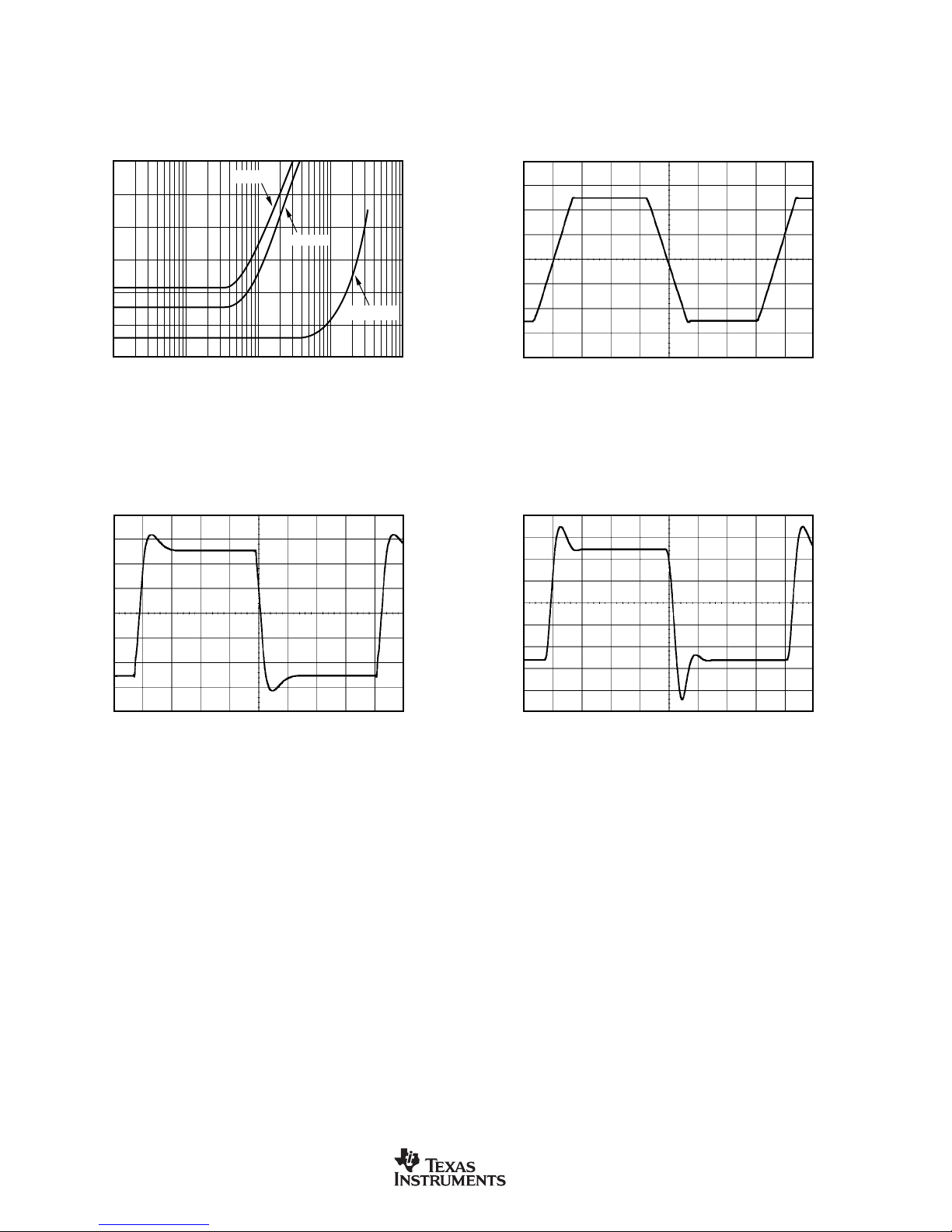
TYPICAL CHARACTERISTICS (CONT)
At TA = +25°C, VS = ±15V, and RL = 2kΩ, unless otherwise noted.
60
50
40
30
Overshoot (%)
20
10
0
SMALL-SIGNAL OVERSHOOT
vs LOAD CAPACITANCE
Gain = –1
Gain = +1
1k10010 10k 100k
Load Capacitance (pF)
SMALL-SIGNAL STEP RESPONSE
G = +1, C
= 0, VS = ±15V
L
Gain = ±10
2V/div
LARGE-SIGNAL STEP RESPONSE
G = +1, CL = 1500pF, V
10µs/div
SMALL-SIGNAL STEP RESPONSE
G = +1, C
= 1500pF, VS = ±15V
L
= +15V
S
20mV/div
1µs/div
20mV/div
1µs/div
8
www.ti.com
OPA277, OPA2277, OPA4277
SBOS079A
APPLICATIONS INFORMATION
The OPA277 series is unity-gain stable and free from unexpected output phase reversal, making it easy to use in a wide
range of applications. Applications with noisy or high impedance power supplies may require decoupling capacitors
close to the device pins. In most cases 0.1µF capacitors are
adequate.
The OPA277 series has very low offset voltage and drift. To
achieve highest performance, circuit layout and mechanical
conditions should be optimized. Offset voltage and drift can
be degraded by small thermoelectric potentials at the op amp
inputs. Connections of dissimilar metals will generate thermal
potential which can degrade the ultimate performance of the
OPA277 series. These thermal potentials can be made to
cancel by assuring that they are equal in both input terminals.
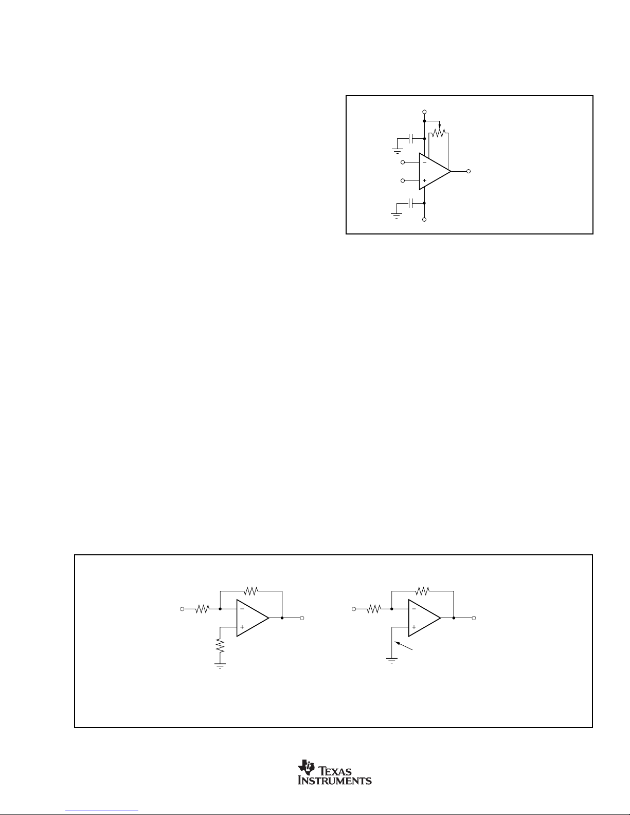
connecting a potentiometer as shown in Figure 1. This
adjustment should be used only to null the offset of the op
amp. This adjustment should not be used to compensate for
offsets created elsewhere in a system since this can introduce additional temperature drift.
V+
Trim Range: Exceeds
0.1µF
2
3
0.1µF
Offset Voltage Specification
20kΩ
7
1
8
OPA277
6
4
Use offset adjust pins only to null
offset voltage of op amp—see text.
OPA277 single op amp only.
• Keep thermal mass of the connections made to the two
input terminals similar.
• Locate heat sources as far as possible from the critical
input circuitry.
• Shield op amp and input circuitry from air currents such as
cooling fans.
OPERATING VOLTAGE
OPA277 series op amp operate from ±2V to ±18V supplies
with excellent performance. Unlike most op amps which are
specified at only one supply voltage, the OPA277 series is
specified for real-world applications; a single limit applies
over the ±5V to ±15V supply range. This allows a customer
operating at V
= ±10V to have the same assured perfor-
S
mance as a customer using ±15V supplies. In addition, key
parameters are assured over the specified temperature range,
–40°C to +85°C. Most behavior remains unchanged through
the full operating voltage range (±2V to ±18V). Parameters
which vary significantly with operating voltage or temperature
are shown in typical performance curves.
OFFSET VOLTAGE ADJUSTMENT
The OPA277 series is laser-trimmed for very low offset
voltage and drift so most circuits will not require external
adjustment. However, offset voltage trim connections are
provided on pins 1 and 8. Offset voltage can be adjusted by
V–
FIGURE 1. OPA277 Offset Voltage Trim Circuit.
INPUT PROTECTION
The inputs of the OPA277 series are protected with 1kΩ
series input resistors and diode clamps. The inputs can
withstand ±30V differential inputs without damage. The protection diodes will, of course, conduct current when the
inputs are over-driven. This may disturb the slewing behavior
of unity-gain follower applications, but will not damage the op
amp.
INPUT BIAS CURRENT CANCELLATION
The input stage base current of the OPA277 series is
internally compensated with an equal and opposite cancellation circuit. The resulting input bias current is the difference
between the input stage base current and the cancellation
current. This residual input bias current can be positive or
negative.
When the bias current is canceled in this manner, the input
bias current and input offset current are approximately the
same magnitude. As a result, it is not necessary to use a bias
current cancellation resistor as is often done with other op
amps (Figure 2). A resistor added to cancel input bias current
errors may actually increase offset voltage and noise.
R
1
Conventional op amp with external bias
current cancellation resistor.
FIGURE 2. Input Bias Current Cancellation.
OPA277, OPA2277, OPA4277
SBOS079A
R
Op Amp
RB = R2 || R
(a)
2
R
1
1
OPA277 with no external bias current
cancellation resistor.
www.ti.com
R
2
OPA277
No bias current
cancellation resistor
(see text)
(b)
9
 Loading...