

Burr Brown Corporation EG1117-2.85 Datasheet
REG1117
®
1
REG1117
REG1117A
800mA and 1A Low Dropout Positive Regulator
1.8V, 2.5V, 2.85V, 3.3V, 5V, and Adjustable
®
FEATURES
● FIXED AND ADJUSTABLE VERSIONS
● 2.85V MODEL FOR SCSI-2 ACTIVE
TERMINATION
● OUTPUT CURRENT:
REG1117: 800mA max
REG1117A: 1A max
● OUTPUT TOLERANCE: ±1% max
● DROPOUT VOLTAGE:
REG1117: 1.2V max at IO = 800mA
REG1117A: 1.3V max at IO = 1 A
● INTERNAL CURRENT LIMIT
● THERMAL OVERLOAD PROTECTION
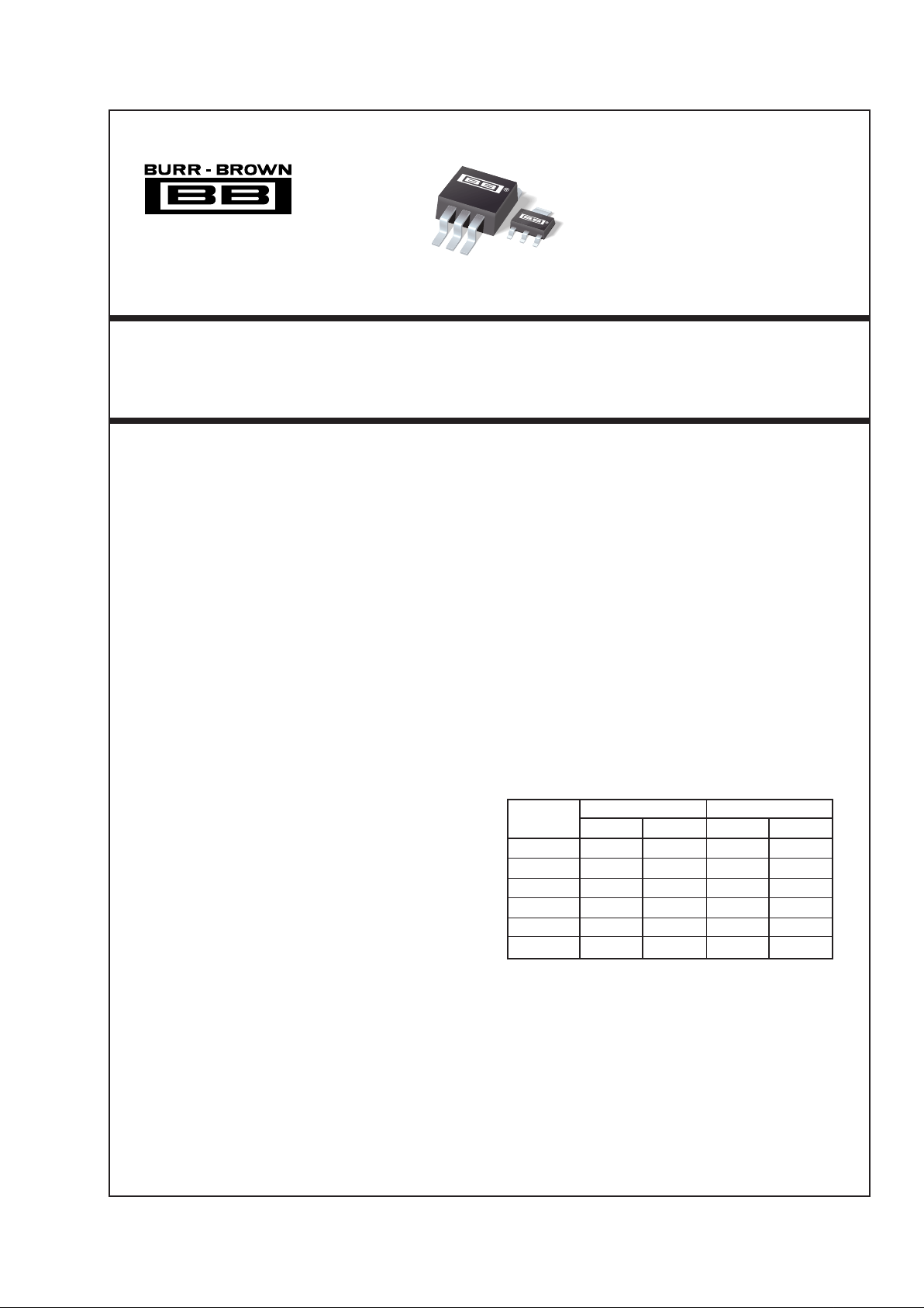
● SOT-223 AND DDPAK SURFACE
MOUNT PACKAGES
APPLICATIONS
● SCSI-2 ACTIVE TERMINATION
● HAND-HELD DATA COLLECTION DEVICES
● HIGH EFFICIENCY LINEAR REGULATORS
● BATTERY POWERED INSTRUMENTATION
● BATTERY MANAGEMENT CIRCUITS FOR
NOTEBOOK AND PALMTOP PCs
● CORE VOLTAGE SUPPLY:
FPGA, PLD, DSP, CPU
DESCRIPTION
The REG1117 is a family of easy-to-use three-terminal voltage regulators. The family includes a variety of
fixed- and adjustable-voltage versions, two currents
(800mA and 1A) and two package types (SOT-223
and DDPAK). See the chart below for available options.
Output voltage of the adjustable versions is set with
two external resistors. The REG1117’s low dropout
voltage allows its use with as little as 1V input-output
voltage differential.
Laser trimming assures excellent output voltage accuracy without adjustment. An NPN output stage allows
output stage drive to contribute to the load current for
maximum efficiency.
REG1117
©
1992 Burr-Brown Corporation PDS-1162J Printed in U.S.A. December, 1999
International Airport Industrial Park • Mailing Address: PO Box 11400, Tucson, AZ 85734 • Street Address: 6730 S. Tucson Blvd., Tucson, AZ 85706 • Tel: (520) 746-1111
Twx: 910-952-1111 • Internet: http://www.burr-brown.com/ • Cable: BBRCORP • Telex: 066-6491 • FAX: (520) 889-1510 • Immediate Product Info: (800) 548-6132
For most current data sheet and other product
information, visit www.burr-brown.com
800mA 1A
VOLTAGE SOT-223 DDPAK SOT-223 DDPAK
1.8V ✔✔
2.5V ✔✔
2.85V ✔
3.3V ✔✔
5V ✔✔
Adj. ✔✔✔
2
®
REG1117
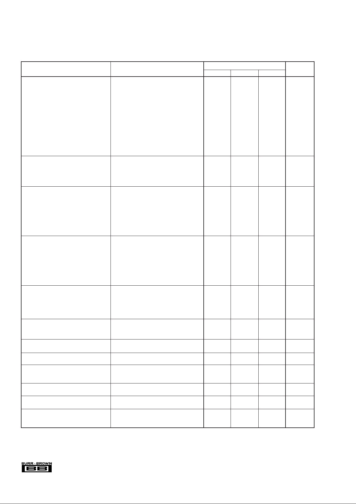
SPECIFICATIONS
At TJ = +25°C, unless otherwise noted.
REG1117, REG1117A
PARAMETER CONDITIONS MIN TYP MAX UNITS
OUTPUT VOLTAGE
REG1117-2.85 I
O
= 10mA, V
IN
= 4.85V 2.820 2.85 2.880 V
Note 1 I
O
= 0 to 800mA, V
IN
= 4.05 to 10V 2.790 2.85 2.910 V
REG1117-3.3 I
O
= 10mA, V
IN
= 5.3V 3.270 3.30 3.330 V
Note 1 I
O
= 0 to 800mA, V
IN
= 4.8 to 10V 3.240 3.30 3.360 V
REG1117-5 I
O
= 10mA, V
IN
= 7V 4.950 5.00 5.050 V
Note 1 I
O
= 0 to 800mA, V
IN
= 6.5 to 10V 4.900 5.00 5.100 V
REG1117A-1.8 I
O
= 10mA, V
IN
= 3.8V 1.782 1.8 1.818 V
Note 1 I
O
= 0 to 1A, V
IN
= 3.8V to 10V 1.764 1.8 1.836 V
REG1117A-2.5 I
O
= 10mA, V
IN
= 4.5V 2.475 2.5 2.525 V
Note 1 I
O
= 0 to 1A, V
IN
= 4.5V to 10V 2.450 2.5 2.550 V
REG1117A-5 I
O
= 10mA, V
IN
= 7V 4.950 5.0 5.050 V
Note 1 I
O
= 0 to 1A, V
IN
= 7V to 10V 4.900 5.0 5.100 V
REFERENCE VOLTAGE
REG1117 (Adjustable) I
O
= 10mA, V
IN
– VO = 2V 1.238 1.250 1.262 V
Note 1 I
O
= 10 to 800mA, V
IN
– VO = 1.4 to 10V 1.225 1.250 1.280 V
REG1117A (Adjustable) I
O
= 10mA, V
IN
– VO = 2V 1.238 1.250 1.262 V
Note 1 I
O
= 10mA to 1A, V
IN
– VO = 1.4 to 10V 1.225 1.250 1.280 V
LINE REGULATION
REG1117-2.85 Note 1 IO = 0, V
IN
= 4.25 to 10V 1 7 mV
REG1117-3.3 Note 1 I
O
= 0, V
IN
= 4.8 to 10V 2 7 mV
REG1117-5 Note 1 I
O
= 0, V
IN
= 6.5 to 15V 3 10 mV
REG1117 (Adjustable) Note 1 I
O
= 10mA, V
IN
– VO = 1.5 to 13.75V 0.1 0.4 %
REG1117A (Adjustable) Note 1 I
O
= 10mA, V
IN
– VO = 1.5 to 13.75V 0.1 0.4 %
REG1117A-1.8 Note 1 I
O
= 0, V
IN
= 3.8V to 10V 1 7 mV
REG1117A-2.5 Note 1 I
O
= 0, V
IN
= 4.5V to 10V 1 7 mV
REG1117A-5.0 Note 1 I
O
= 0, V
IN
= 7V to 15V 3 10 mV
LOAD REGULATION
REG1117-2.85 Note 1 IO = 0 to 800mA, V
IN
= 4.25V 2 10 mV
REG1117-3.3 Note 1 I
O
= 0 to 800mA, V
IN
= 4.8V 3 12 mV
REG1117-5 Note 1 I
O
= 0 to 800mA, V
IN
= 6.5V 3 15 mV
REG1117
(Adjustable) Note 1, 2 IO = 10 to 800mA, V
IN
– VO = 3V 0.1 0.4 %
REG1117A
(Adjustable) Note 1, 2 IO = 10mA to 1A, V
IN
– VO = 3V 0.1 0.4 %
REG1117A-1.8 I
O
= 0 to 1A, V
IN
= 3.8V 2 10 mV
REG1117A-2.5 I
O
= 0 to 1A, V
IN
= 4.5V 2 10 mV
REG1117A-5 I
O
= 0 to 1A, V
IN
= 7.0V 3 15 mV
DROPOUT VOLTAGE Note 3
All Models Note 1 IO = 100mA 1.00 1.10 V
Note 1 I
O
= 500mA 1.05 1.15 V
REG1117 Models Note 1 I
O
= 800mA 1.10 1.20 V
REG1117A I
O
= 1A 1.2 1.30 V
Note 1 I
O
= 1A 1.2 1.55 V
CURRENT LIMIT
REG1117 Models V
IN
– VO = 5V 800 950 1200 mA
REG1117A V
IN
– VO = 5V 1000 1250 1600 mA
MINIMUM LOAD CURRENT
Adjustable Models Note 1, 2 V
IN
– VO = 13.75V 1.7 5 mA
QUIESCENT CURRENT
Fixed-Voltage Models Note 1 V
IN
– VO = 5V 4 10 mA
Adjust Pin Current Note 1, 2 I
O
= 10mA, V
IN
– VO = 1.4 to 10V 50 120 µA
vs Load Current, REG1117 Note 1 I
O
= 10mA to 800mA, V
IN
– VO = 1.4 to 10V 0.5 5 µA
vs Load Current, REG1117A Note 1 I
O
= 10mA to 1A, V
IN
– VO = 1.4 to 10V 0.5 5 µA
THERMAL REGULATION
All Models Note 4 30ms Pulse 0.01 0.1 %/W
RIPPLE REJECTION
All Models f = 120Hz, V
IN
– V
OUT
= 3V+1VPP Ripple 62 dB
TEMPERATURE DRIFT
Fixed-Voltage Models T
J
= 0°C to +125°C 0.5 %
Adjustable Models T
J
= 0°C to +125°C2%
REG1117
®
3
LONG-TERM STABILITY
All Models T
A
= +125°C, 1000Hr 0.3 %
OUTPUT NOISE
r ms Noise, All Models f = 10Hz to 10kHz 0.003 %
THERMAL RESISTANCE
Operating Junction Temperature Range 0 +125 °C
Storage Range –65 +150 °C
Thermal Resistance,
θ
JC
(Junction-to-Case at Tab)
3-Lead SOT-223 Surface-Mount 15 °C/W
3-Lead DDPAK Surface-Mount f > 50Hz 2 °C/W
dc 3 °C/W
Thermal Resistance,
θ
JA
(Junction-to-Case at Tab)
3-Lead DDPAK Surface-Mount No Heat Sink 65 °C/W
The information provided herein is believed to be reliable; however, BURR-BROWN assumes no responsibility for inaccuracies or omissions. BURR-BROWN assumes
no responsibility for the use of this information, and all use of such information shall be entirely at the user's own risk. Prices and specifications are subject to change
without notice. No patent rights or licenses to any of the circuits described herein are implied or granted to any third party. BURR-BROWN does not authorize or warrant
any BURR-BROWN product for use in life support devices and/or systems.
NOTES: (1) Specification applies over the full operating Junction temperature range, 0°C to 125°C. (2) REG1117 and REG1117A adjustable versions require a
minimum load current for ±3% regulation. (3) Dropout voltage is the Input voltage minus output voltage that produces a 1% decrease in output voltage.
(4) Percentage change in unloaded output voltage before vs after a 30ms power pulse of I
O
= 800mA (REG1117 models), IO = 1A (REG1117A), VIN – VO = 1.4V
(Reading taken 10ms after pulse).
SPECIFICATIONS (cont.)
At TJ = +25°C, unless otherwise noted.
REG1117, REG1117A
PARAMETER CONDITIONS MIN TYP MAX UNITS
ABSOLUTE MAXIMUM RATINGS
(1)
Power Dissipation ........................................................... Internally Limited
Input Voltage........................................................................................ 15V
Operating Junction Temperature Range............................. 0°C to +125°C
Storage Temperature Range .......................................... –65°C to +150°C
Lead Temperature (soldering, 10s)
(2)
............................................ +300°C
NOTE: (1) Stresses above these ratings may cause permanent damage. (2) See
“Soldering Methods.”
ELECTROSTATIC
DISCHARGE SENSITIVITY
This integrated circuit can be damaged by ESD. Burr-Brown
recommends that all integrated circuits be handled with
appropriate precautions. Failure to observe proper handling
and installation procedures can cause damage.
ESD damage can range from subtle performance degradation to complete device failure. Precision integrated circuits
may be more susceptible to damage because very small
parametric changes could cause the device not to meet its
published specifications.
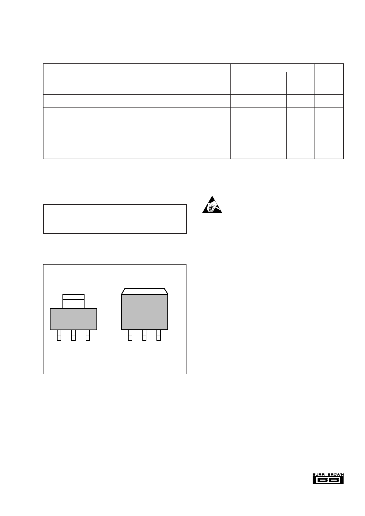
Plastic SOT-223
Plastic DDPAK
Tab is V
OUT
V
IN
V
OUT
Ground
(Adj.)
(1)
Tab is
V
OUT
V
IN
V
OUT
Ground
(Adj.)
(1)
NOTE: (1) Adjustable-Voltage Model.
CONNECTION DIAGRAM
Front View
 Loading...