

Burr Brown Corporation DSD1700E-2K, DSD1700E Datasheet
®
DSD1700
©
1999 Burr-Brown Corporation PDS-1555A Printed in U.S.A. December, 1999
Direct Stream Digital™ (DSD™)
TM
Audio
DIGITAL-TO-ANALOG CONVERTER
International Airport Industrial Park • Mailing Address: PO Box 11400, Tucson, AZ 85734 • Street Address: 6730 S. Tucson Blvd., Tucson, AZ 85706 • Tel: (520) 746-1111
Twx: 910-952-1111 • Internet: http://www.burr-brown.com/ • Cable: BBRCORP • Telex: 066-6491 • FAX: (520) 889-1510 • Immediate Product Info: (800) 548-6132
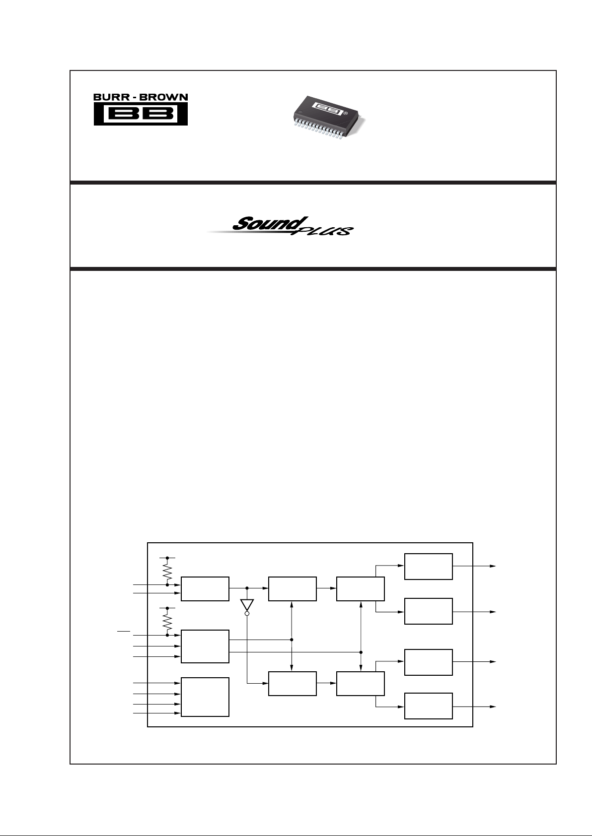
DESCRIPTION
The DSD1700 is a unique digital-to-analog converter
designed for DSD audio applications. The DSD1700
consists of a single-channel, 8-tap analog FIR filter
constructed using a double differential circuit architecture, ensuring excellent dynamic performance and
high power- supply noise rejection. The DSD1700
also includes the necessary logic required to interface
directly to a DSD decoder IC.
The overall features and performance of the DSD1700
make it an ideal choice for high-performance Super
Audio CD players and DSD studio applications.
FEATURES
● DIRECT TRANSFER OF DSD DATA
STREAM TO ANALOG OUTPUT SIGNAL
● DUAL DIFFERENTIAL ANALOG FIR FILTER
● DIRECT, CMOS LOGIC INTERFACE TO
DSDTM DECODER IC
Data Clock: 2.8224 MHz (64 • 44.1kHz)
System Clock: 11.2896 MHz (256 • 44.1kHz)
● EXCELLENT DYNAMIC PERFORMANCE
THD+N: 0.001% (typ)
Dynamic Range: 110dB (typ)
SNR: 110dB (typ)
Frequency Response (–3dB): 100kHz
● SINGLE +5V SUPPLY OPERATION
● SMALL 28-LEAD SSOP PACKAGE
APPLICATIONS
● SUPER AUDIO CD (SACD™) PLAYERS
● PROFESSIONAL DSD PROCESSORS
● PROFESSIONAL DSD CONSOLES
For most current data sheet and other product
information, visit www.burr-brown.com
DSD I/F
PHASE
DATA
RST
DCK
SCK
V
DD
DGND
V
CC
AGND
Duty
Generator
Duty
Generator
Shift Register
(HOT)
Analog FIR
(HOT/P)
Analog FIR
(HOT/N)
Analog FIR
(COLD/N)
Analog FIR
(COLD/P)
Shift Register
(COLD)
V
DD
Timing
Generator
Power
Supply
V
DD
I
OUT
HP
I
OUT
HN
I
OUT
CP
I
OUT
CN
DSD1700
All trademarks are property of their respective owners.
2
®
DSD1700
The information provided herein is believed to be reliable; however, BURR-BROWN assumes no responsibility for inaccuracies or omissions. BURR-BROWN
assumes no responsibility for the use of this information, and all use of such information shall be entirely at the user’s own risk. Prices and specifications are subject
to change without notice. No patent rights or licenses to any of the circuits described herein are implied or granted to any third party. BURR-BROWN does not
authorize or warrant any BURR-BROWN product for use in life support devices and/or systems.
SPECIFICATIONS
All specifications TA = +25°C, VDD = VCC = 5.0V, fS = 44.1kHz, data clock = 64fS, system clock = 256fS, unless otherwise specified. (Although the sampling frequency
of Direct Stream Digital is 2.8224MHz, for convenience, in this specification sheet, it is described that the sampling frequency (f
S
) is 44.1kHz and the 2.8224MHz
clock is 64f
S
).
DSD1700E
PARAMETER CONDITIONS MIN TYP MAX UNITS
INPUT CLOCK
Data Clock Frequency (DCK) 64f
S
2.8224 MHz
System Clock Frequency (SCK) 256f
S
11.2896 MHz
SCK AC REQUIREMENT
(1)
Input Clock Duty Cycle 50 %
DIGITAL INPUT
High Level Input Voltage V
IH
0.7V
DD
V
Low Level Input Voltage V
IL
0.3V
DD
V
High Level Input Current I
IH
±10 µA
Low Level Input Current I
IL
(2)
±10 µA
I
IL
(3)
–120 µA
ANALOG OUTPUT
(5)
Full-Scale Voltage 4.1V
CC
Vp-p
Gain Error ±4 ±10 % of FSR
Offset Error ±0.1 ±1 % of FSR
Output Impedance
(4)
2kΩ
DYNAMIC PERFORMANCE
(5)
THD+N, V
OUT
= 0dB with 30kHz GIC Filter 0.001 %
Dynamic Range with 30kHz GIC Filter 110 dB
Signal-to-Noise Ratio with 30kHz GIC Filter 110 dB
Frequency Response, –3dB 100 kHz
POWER SUPPLY REQUIREMENTS
Voltage Range V
CC
, V
DD
4.5 5 5.5 VDC
Supply Current I
CC+IDD
VCC = VDD = 5.0V 5.5 8.0 mA
Power Dissipation V
CC
= VDD = 5.0V 27.5 40 mW
TEMPERATURE RANGE
Operating –25 +85 °C
Storage –55 +125 °C
Thermal Resistance θ
JA
28-Pin SSOP 100 °C/W
NOTES: (1) See description of system clock in the Functional Description section of this data sheet. (2) Pins 26, 27, 28: DATA. DCK. SCK. (3) Pins 3, 4: RST, PHASE
(with internal pull-up). (4) Pins 13, 14, 15, 16: I
OUT
HN, I
OUT
CP, I
OUT
CN, I
OUT
HP. (5) Measure DSD signal modulated f
SIG
= 1kHz with 50% scaling factor through
standard differential to single-ended converter (see Figure 10) using Audio Precision System II in rms mode with 20kHz LPF and 400Hz HPF.
3
®
DSD1700
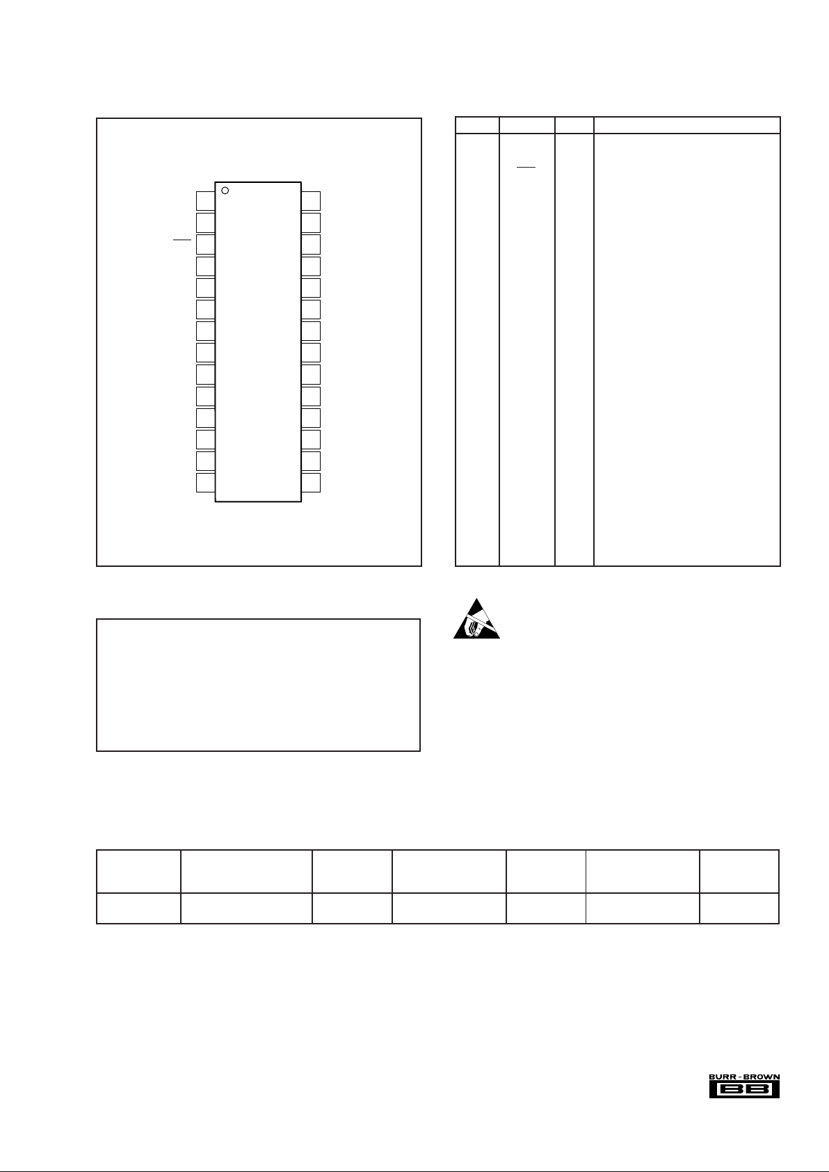
PIN CONFIGURATION
ELECTROSTATIC
DISCHARGE SENSITIVITY
This integrated circuit can be damaged by ESD. Burr-Brown
recommends that all integrated circuits be handled with
appropriate precautions. Failure to observe proper handling
and installation procedures can cause damage.
ESD damage can range from subtle performance degradation to complete device failure. Precision integrated circuits
may be more susceptible to damage because very small
parametric changes could cause the device not to meet its
published specifications.
Supply Voltage
(2)
.............................................................................. +6.5V
Supply Voltage Differences
(3)
........................................................... ±0.1V
Ground Voltage Differences
(4)
.......................................................... ±0.1V
Digital Input Voltage ................................................... –0.3V to V
DD
+0.3V
Input Current (any pins except supplies) ....................................... ±10mA
Operating Temperature .................................................... –25°C to +85°C
Storage Temperature .....................................................–55°C to +125°C
Junction Temperature .................................................................... +150°C
Lead Temperature (soldering, 5s) ................................................. +260°C
Package Temperature (IR reflow, peak, 10s) ............................... +235°C
NOTE: (1) Stresses above these ratings may cause permanent damage.
Exposure to absolute maximum conditions for extended periods may degrade
device reliability. (2) V
CC
, VDD. (3) Among VCC, VDD. (4) Among AGND, DGND.
ABSOLUTE MAXIMUM RATINGS
(1)
Top View SSOP
PACKAGE SPECIFIED
DRAWING TEMPERATURE PACKAGE ORDERING TRANSPORT
PRODUCT PACKAGE NUMBER RANGE MARKING NUMBER
(1)
MEDIA
DSD1700E 28-Lead SSOP 324 0°C to +70°C DSD1700E DSD1700E Rails
"""""DSD1700E/2K Tape and Reel
NOTE: (1) Models with a slash (/) are available only in Tape and Reel in the quantities indicated (e.g., /2K indicates 2000 devices per reel). Ordering 2000 pieces
of “DSD1700E/2K” will get a single 2000-piece Tape and Reel.
PACKAGE/ORDERING INFORMATION
DGND
V
DD
RST
PHASE
AGND
V
CC
AGND
V
CC
V
CC
AGND
V
CC
AGND
I
OUT
HN
I
OUT
CP
SCK
DCK
DATA
AGND
V
CC
AGND
V
CC
V
CC
AGND
V
CC
AGND
AGND
I
OUT
HP
I
OUT
CN
1
2
3
4
5
6
7
8
9
10
11
12
13
14
28
27
26
25
24
23
22
21
20
19
18
17
16
15
DSD1700
PIN NAME I/O DESCRIPTION
1 DGND — Digital Ground
2V
DD
— Digital Power Supply: +5V
3 RST IN Reset Control Input, Active LOW
(1)
4 PHASE IN Select data phase
(LOW = Normal; HIGH = Invert)
5 AGND — Analog Ground
6V
CC
— Analog Power Supply: +5V
7 AGND — Analog Ground
8V
CC
— Analog Power Supply: +5V
9V
CC
— Analog Power Supply: +5V
10 AGND — Analog Ground
11 V
CC
— Analog Power Supply: +5V
12 AGND — Analog Ground
13 I
OUT
HN OUT Analog Output from DAC (Hot Negative)
14 I
OUT
CP OUT Analog Output from DAC (Cold Positive)
15 I
OUT
CN OUT Analog Output from DAC (Cold Negative)
16 I
OUT
HP OUT Analog Output from DAC (Hot Positive)
17 AGND — Analog Ground
18 AGND — Analog Ground
19 V
CC
— Analog Power Supply: +5V
20 AGND — Analog Ground
21 V
CC
— Analog Power Supply: +5V
22 V
CC
— Analog Power Supply: +5V
23 AGND — Analog Ground
24 V
CC
— Analog Power Supply: +5V
25 AGND — Analog Ground
26 DATA IN Direct Stream Digital Data Input
27 DCK IN Data Clock Input
28 SCK IN System Clock Input
NOTE: (1) With internal pull-up resistor
PIN ASSIGNMENTS
 Loading...