

Burr Brown Corporation DRV102T, DRV102F-500, DRV102F Datasheet
®
For most current data sheet and other product
information, visit www.burr-brown.com
PWM SOLENOID/VALVE DRIVER
DRV102
D
RV102
DRV102
FEATURES
● HIGH OUTPUT DRIVE: 2.7A
● WIDE SUPPLY RANGE: +8V to +60V
● COMPLETE FUNCTION
PWM Output
Internal 24kHz Oscillator
Digital Control Input
Adjustable Delay and Duty Cycle
Over/Under Current Indicator
● FULLY PROTECTED
Thermal Shutdown with Indicator
Internal Current Limit
● POWER PACKAGES: 7-Lead TO-220 and
7-Lead Surface-Mount DDPAK
DESCRIPTION
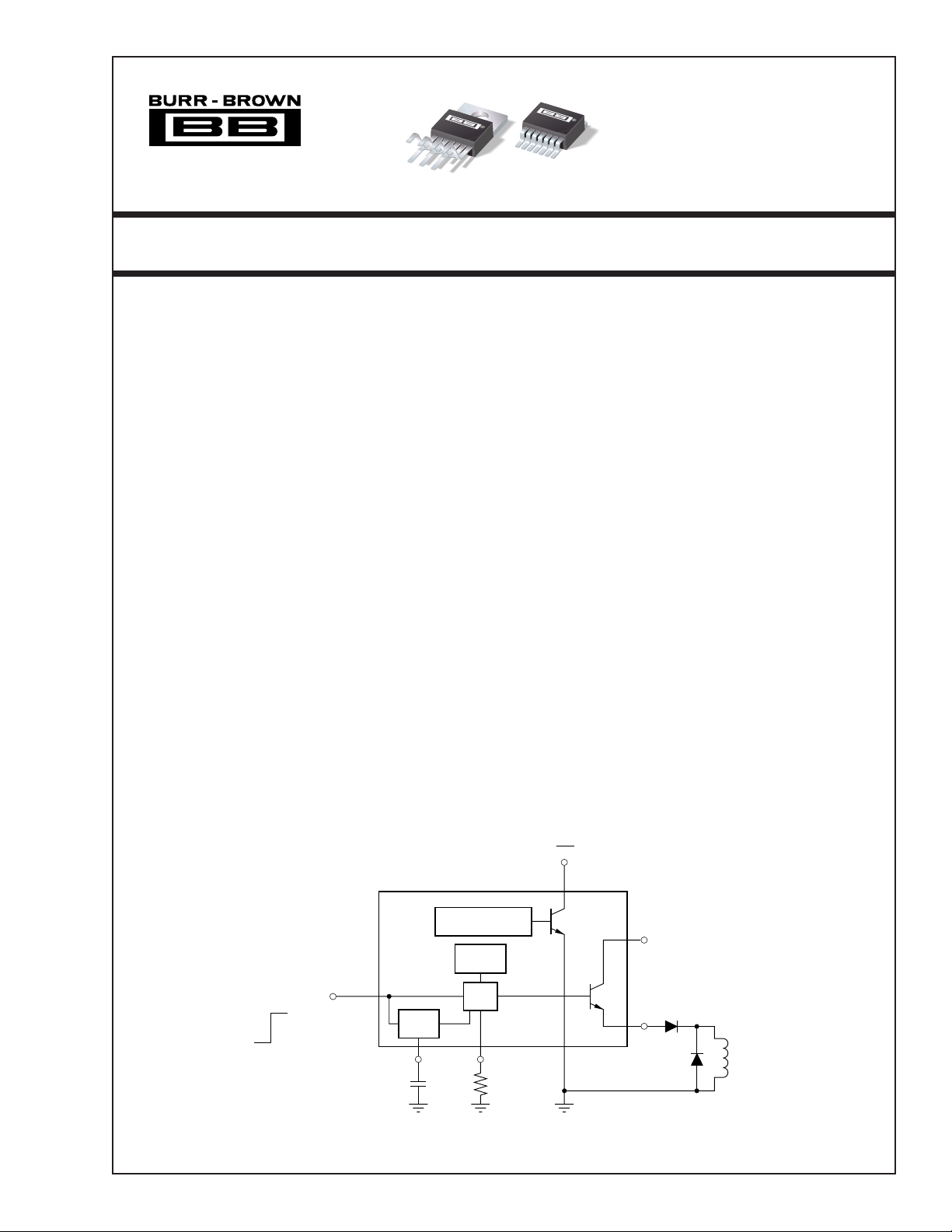
The DRV102 is a high-side power switch employing
a pulse-width modulated (PWM) output. Its rugged
design is optimized for driving electromechanical devices such as valves, solenoids, relays, actuators, and
positioners. The DRV102 is also ideal for driving
thermal devices such as heaters and lamps. PWM
operation conserves power and reduces heat rise in the
device, resulting in higher reliability. In addition, adjustable PWM allows fine control of the power delivered to the load. Time from dc output to PWM output
is externally adjustable.
APPLICATIONS
● ELECTROMECHANICAL DRIVER:
Solenoids Positioners
Actuators
Valves Clutches/Brakes
● SOLENOID OVERHEAT PROTECTORS
● FLUID AND GAS FLOW CONTROLLERS
● PART HANDLERS
● ELECTRICAL HEATERS/COOLERS
● MOTOR SPEED CONTROLLERS
● INDUSTRIAL CONTROL
● FACTORY AUTOMATION
● MEDICAL ANALYSIS
● PHOTOGRAPHIC PROCESSING
The DRV102 can be set to provide a strong initial
closure, automatically switching to a “soft” hold mode
for power savings. Duty cycle can be controlled by a
resistor, analog voltage, or digital-to-analog converter
for versatility. A flag output indicates thermal shutdown and over/under current limit. A wide supply
range allows use with a variety of actuators.
The DRV102 is available in 7-lead staggered TO-220
package and a 7-lead surface-mount DDPAK plastic
power package. It operates from –55°C to +125°C.
Flag
High Power Relays/Contactors
7
(1)
4
DRV102
5
V
6
Out
(Gnd electrically
connected to tab)
(+8V to +60V)
S
Load
Thermal Shutdown
Over/Under Current
24kHz
Oscillator
Input
1
On
(TTL-Compatible)
Off
International Airport Industrial Park • Mailing Address: PO Box 11400, Tucson, AZ 85734 • Street Address: 6730 S. Tucson Blvd., Tucson, AZ 85706 • Tel: (520) 746-1111
Twx: 910-952-1111 • Internet: http://www.burr-brown.com/ • Cable: BBRCORP • Telex: 066-6491 • FAX: (520) 889-1510 • Immediate Product Info: (800) 548-6132
©
1998 Burr-Brown Corporation PDS-1471B Printed in U.S.A. March, 1999
Delay
PWM
23
Delay
Adjust
Gnd
Duty Cycle
Adjust
SPECIFICATIONS
At TC = +25°C, VS = +24V, load = series diode MUR415 and 100Ω, and 4.99kΩ Flag pull-up to +5V, unless otherwise noted.
DRV102T, F
PARAMETER CONDITIONS MIN TYP MAX UNITS
OUTPUT
Output Saturation Voltage, Source I
Current Limit 2 2.7 3.4 A
Under-Scale Current 16 mA
Leakage Current Output Transistor Off, V
DIGITAL CONTROL INPUT
V
Low (output disabled) 0 +1.2 V
CTR
V
High (output enabled) +2.2 V
CTR
I
Low (output disabled) V
CTR
I
High (output enabled) V
CTR
(1)
Propagation Delay: On-to-Off 0.9 µs
Off-to-On 1.8 µs
DELAY TO PWM
Delay Equation
Delay Time C
Minimum Delay Time
(3)
(4)
(5)
DUTY CYCLE ADJUST
Duty Cycle Range 10 to 90 %
Duty Cycle Accuracy 49% Duty Cycle, R
vs Supply Voltage 49% Duty Cycle, VS = 8V to 60V ±1 ±5%
Nonlinearity
(6)
20% to 80% Duty Cycle ±2 % FSR
DYNAMIC RESPONSE
Output Voltage Rise Time V
Output Voltage Fall Time VO = 90% to 10% of V
Oscillator Frequency 19 24 29 kHz
FLAG
Normal Operation 20kΩ Pull-Up to +5V, I
(7)
Fault
Sink Current V
Under-Current Flag: Set 5.2 µs
Reset 11 µs
Over-Current Flag: Set 5.2 µs
Reset 11.5 µs
THERMAL SHUTDOWN
Junction Temperature
Shutdown +165 °C
Reset from Shutdown +150 °C
POWER SUPPLY
Specified Operating Voltage +24 V
Operating Voltage Range +8 +60 V
Quiescent Current I
TEMPERATURE RANGE
Specified Range –55 +125 °C
Storage Range –55 +125 °C
Thermal Resistance,
θ
JC
7-Lead DDPAK, 7-Lead TO-220 3 °C/W
Thermal Resistance,
θ
JA
7-Lead DDPAK, 7-Lead TO-220 No Heat Sink 65 °C/W
NOTES: (1) Logic high enables output (normal operation). (2) Negative conventional current flows out of the terminals. (3) Constant dc output to PWM (pulse-width
modulated) time. (4) Maximum delay is determined by an external capacitor. Pulling the Delay Adjust pin low corresponds to an infinite (continuous) delay.
(5) Connecting the Delay Adjust pin to +5V reduces delay time to 3µs. (6) V
over-current, or under-current conditions.
= 1A +1.7 +2.2 V
O
IO = 0.1A +1.3 +1.7 V
= +60V, VO = 0V ±0.01 ±2mA
S
= 0V –80
CTR
= +5V 20
CTR
(2)
(2)
S
dc to PWM Mode
Delay to PWM ≈ CD • 106 (CD in F) s
= 0.1µF 80 97 110 ms
D
CD = 0 15 µs
= 25.5kΩ±1 ±7%
PWM
= 10% to 90% of V
O
S
S
< 1.5A +4 +4.9 V
O
0.25 2.5 µs
0.25 2.5 µs
Sinking 1mA +0.2 +0.4 V
= 0.4V 2 mA
FLAG
= 0 6.5 9 mA
O
at pin 3 to percent of duty cycle at pin 6. (7) A fault results from over-temperature,
IN
V
µA
µA
The information provided herein is believed to be reliable; however, BURR-BROWN assumes no responsibility for inaccuracies or omissions. BURR-BROWN assumes
no responsibility for the use of this information, and all use of such information shall be entirely at the user’s own risk. Prices and specifications are subject to change
without notice. No patent rights or licenses to any of the circuits described herein are implied or granted to any third party. BURR-BROWN does not authorize or warrant
any BURR-BROWN product for use in life support devices and/or systems.
®
DRV102
2
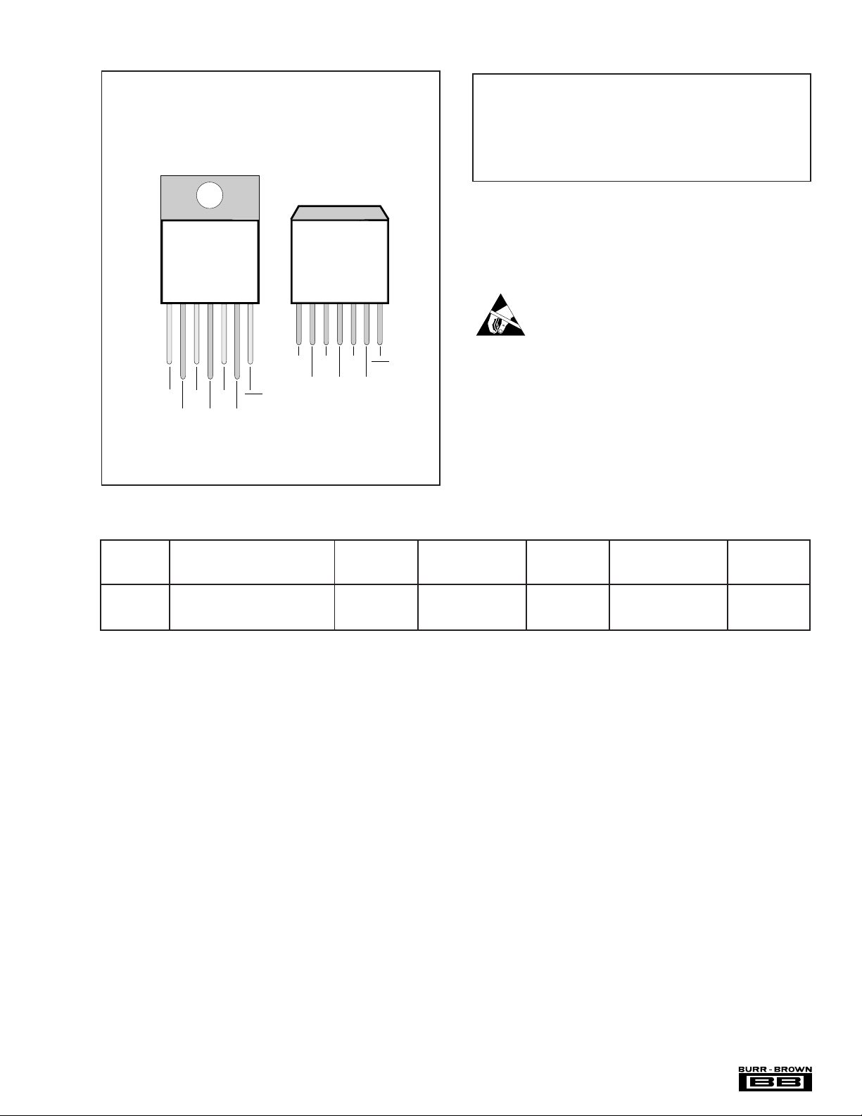
CONNECTION DIAGRAMS
Top Front View TO-220, DDPAK
7-Lead
Stagger-Formed
TO-220
7-Lead
DDPAK
Surface-Mount
ABSOLUTE MAXIMUM RATINGS
Supply Voltage, V
Input Voltage .......................................................................... –0.2V to V
PWM Adjust Input ................................................ –0.2V to VS (24V max)
Delay Adjust Input ................................................ –0.2V to V
Operating Temperature Range ...................................... –55°C to +125°C
Storage Temperature Range ......................................... –55°C to +125°C
Junction Temperature .................................................................... +150°C
Lead Temperature (soldering, 10s)
NOTES: (1) Stresses above these ratings may cause permanent damage.
Exposure to absolute maximum conditions for extended periods may degrade device reliability. (2) Vapor-phase or IR reflow techniques are recommended for soldering the DRV102F surface-mount package. Wave soldering
is not recommended due to excessive thermal shock and “shadowing” of
nearby devices.
.............................................................................. 60V
S
(2)
........................................... +300°C
(1)
S
(24V max)
S
1234
7
5
6
1234
6 7
5
ELECTROSTATIC
DISCHARGE SENSITIVITY
In
PWM
V
Flag
S
Delay
In
Delay
NOTE: Tabs are electrically connected to ground (pin 4).
PWM
Gnd Out
V
S
Flag
Gnd Out
PACKAGE/ORDERING INFORMATION
PACKAGE SPECIFIED
DRAWING TEMPERATURE PACKAGE ORDERING TRANSPORT
PRODUCT PACKAGE NUMBER
DRV102T 7-Lead Stagger-Formed TO-220 327 –55°C to +125°C DRV102T DRV102T Rails
DRV102F 7-Lead DDPak Surface Mount 328 –55°C to +125°C DRV102F DRV102F Rails
" " " " " DRV102F/500 Tape and Reel
NOTES: (1) For detailed drawing and dimension table, please see end of data sheet, or Appendix C of Burr-Brown IC Data Book. (2) Models with a slash (/ )
are available only in Tape and Reel in the quantities indicated (e.g., /500 indicates 500 devices per reel). Ordering 500 pieces of “DRV102F/500” will get a single
500-piece Tape and Reel. For detailed Tape and Reel mechanical information, refer to Appendix B of Burr-Brown IC Data Book.
(1)
This integrated circuit can be damaged by ESD. Burr-Brown
recommends that all integrated circuits be handled with
appropriate precautions. Failure to observe proper handling and
installation procedures can cause damage.
ESD damage can range from subtle performance degradation to
complete device failure. Precision integrated circuits may be more
susceptible to damage because very small parametric changes
could cause the device not to meet its published specifications.
RANGE MARKING NUMBER
(2)
MEDIA
®
3
DRV102
PIN DESCRIPTIONS
PIN # NAME DESCRIPTION
Pin 1 Input The input is compatible with standard TTL levels. The device output becomes enabled when the input voltage is driven above
Pin 2 Delay Adjust This pin sets the duration of the initial 100% duty cycle before the output goes into PWM mode. Leaving this pin floating results
Pin 3 Duty Cycle Adjust Internally, this pin connects to the input of a comparator and a 19kΩ resistor to ground. It is driven by a 200µA current source
(PWM) from V
Pin 4 Ground This pin is electrically connected to the package tab. It must be connected to system ground for the DRV102 to function. It
Pin 5 V
S
Pin 6 Out The output is the emitter of a power npn with the collector connected to V
Pin 7 Flag Normally high (active low), the Flag signals either an over-temperature, over-current, or under-current fault. The over/under-
the typical switching threshold, 1.7V. Below this level, the output is disabled. With no connection to the pin, the input level rises
to 3.4V. Input current is 20µA when driven high and 80µA with the input low. The input may be driven to the power supply (V
without damage.
in a delay of approximately 15µs, which is internally limited by parasitic capacitance. Minimum delay may be reduced to less
than 3µs by tying the pin to 5V. This pin connects internally to a 3µA current source from V
When the pin voltage is below 3V, the output device is 100% on. The PWM oscillator is not synchronized to the Input (pin 1),
and to a 3V threshold comparator.
S
so the first pulse may be extended by any portion of the programmed duty cycle.
. The voltage at this node linearly sets the duty cycle. Duty cycle can be programmed with a resistor, analog voltage,
S
or output of a D/A converter. The active voltage range is from 0.55V to 3.7V to facilitate the use of single-supply control
electronics. At 0.56V (or R
frequency is a constant 24kHz.
= 4.4kΩ), duty cycle is near 90%. Swing to ground should be limited to no lower than 0.1V. PWM
PWM
carries the 6.5mA quiescent current.
This is the power supply pin. Operating range is +8V to +60V.
. Low power dissipation in the DRV102 is obtained
by low saturation voltage and fast switching transitions. Rise time is less than 250ns, fall time depends on load impedance.
S
A flyback diode is (D1) needed with inductive loads to conduct the load current during the off cycle. The external diode should
be selected for low forward voltage. The internal clamp diode provides protection but should not be used to conduct load
currents. An additional diode (D2), located in series with Out pin, is required for inductive loads.
current flags are true only when the output is on (constant dc output or the “on” portion of PWM mode). A thermal fault (thermal
shutdown) occurs when the die surface reaches approximately 165°C and latches until the die cools to 150°C. Its output
requires a pull-up resistor. It can typically sink two milliamps, sufficient to drive a low-current LED.
)
S
LOGIC BLOCK DIAGRAM
DRV102
Input
On
Off
1
Thermal
Shutdown
Over/Under Current
PWM
Delay
23
C
D
R
PWM
Flag
7
Gnd 4
5
(+8V to +60V)
V
S
(2)
6
Out
D
2
D
1
Load
(1)
NOTES: (1) Schottky Power Rectifier for low
power dissipation. (2) Schottky or appropriately
rated silicon diode.
®
DRV102
4
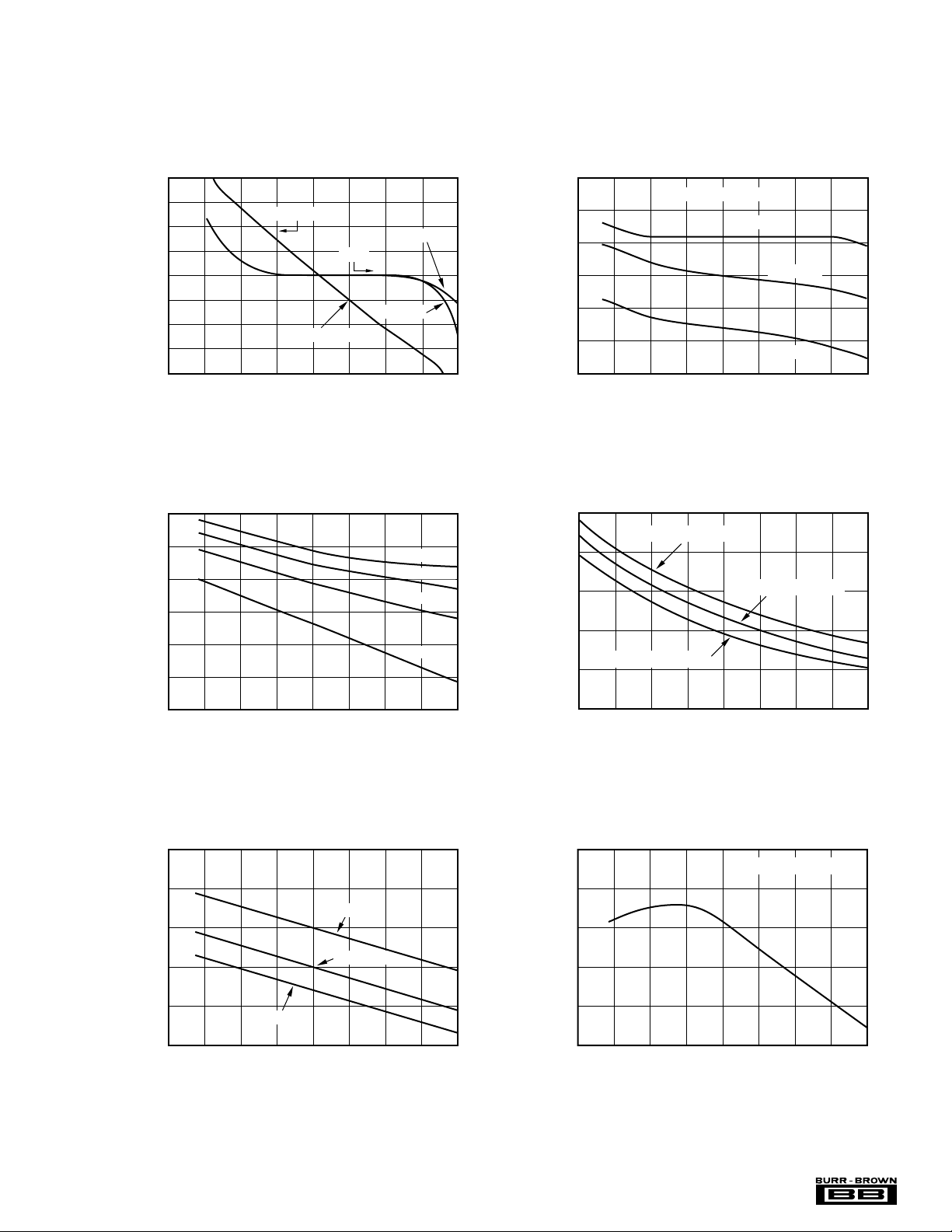
TYPICAL PERFORMANCE CURVES
CURRENT LIMIT vs TEMPERATURE
–75 –50 –25 0 25 50 75 100 125
Temperature (°C)
Current Limit (mA)
3.25
3
2.75
2.5
2.25
2
VS = +60V, Load = 5Ω
VS = +24V, Load = 5Ω
VS = +8V, Load = 1Ω
At TC = +25°C and VS = +24V, unless otherwise noted.
DUTY CYCLE and DUTY CYCLE ERROR vs VOLTAGE
90
80
70
60
50
40
Duty Cycle (%)
30
20
10
0 0.5 1.0 1.5 2.0 2.5 3.0 3.5 4.0
OUTPUT SATURATION VOLTAGE vs TEMPERATURE
2.25
2
1.75
1.5
Duty Cycle
IO = 0.1A to 1A
V
PWM
Error
IO = 1A
(V)
IO = 0.1A
IO = 2A
IO = 1.5A
IO = 1A
8
6
4
2
0
–2
Duty Cycle Error (%)
–4
–6
–8
54
53
52
51
50
Duty Cycle (%)
49
48
–75 –50 –25 0 25 50 75 100 125
DUTY CYCLE vs TEMPERATURE
R
= 25.5kΩ
PWM
VS = +8V
VS = +24V
VS = +60V
Temperature (°C)
1.25
Saturation Voltage (V)
1
0.75
–75 –50 –25 0 25 50 75 100 125
Temperature (°C)
8
7.5
7
6.5
Quiescent Current (mA)
6
5.5
QUIESCENT CURRENT vs TEMPERATURE
VS = +60V
VS = +24V
VS = +8V
–75 –50 –25 0 25 50 75 100 125
Temperature (°C)
IO = 0.1A
20
18
16
14
12
Under-Scale Current (mA)
10
UNDER-SCALE CURRENT vs TEMPERATURE
VS = +8V to +60V
–75 –50 –25 0 25 50 75 100 125
Temperature (°C)
®
5
DRV102
TYPICAL PERFORMANCE CURVES (CONT)
At TC = +25°C and VS = +24V, unless otherwise noted.
(VS = +60V, CD = 220pF, R
60V
OUT
40V
V
20V
0
4V
2V
FLAG
V
0
(VS = +60V, CD = 120pF, R
60V
40V
OUT
V
20V
0
1A
0.5A
SUPPLY
0
I
Inductive load ramp current
FLAG OPERATION
OVER-CURRENT LIMIT
= 25.5kΩ, Load = 350mH || 47Ω)
PWM
Onset of current limit where
V
begins to drop
OUT
Flag only set during
constant output mode
or “ON” portion of
PWM mode
50µs/div
DC TO PWM MODE
DRIVING INDUCTIVE LOAD
= 30.1kΩ, Load = 350mH)
PWM
(VS = +60V, CD = 120pF, R
60V
IN
40V
V
20V
0
4V
2V
FLAG
V
0
Constant Output
TYPICAL SOLENOID CURRENT WAVEFORM
(VS = +60V, CD = 0.1µF, R
4V
IN
0
V
Solenoid
Motion
Period
1A
0.5A
0
Solenoid Current
FLAG OPERATION
UNDER-CURRENT
= 25.5kΩ, No Load)
PWM
Flag only on during constant output
or “ON” portion of PWM mode
PWM Mode
50µs/div
= 30.1kΩ, Load = 350mH)
PWM
{
PWM Mode
Solenoid Closure
FLAG
V
OUT
I
5V
2.5V
3A
2A
1A
50µs/div
25ms/div
CURRENT LIMIT REPSONSE
(Load = 1Ω, 2kΩ pull-up to +5V on Flag pin)
OSCILLATOR FREQUENCY vs TEMPERATURE
24.2
24.0
0
VS = +8V
23.8
23.6
0
Oscillator Frequency (kHz)
VS = +60V
23.4
10µs/div
–75 –55 –35 –15 5 25 45 65 85 105 125
Temperature (°C)
®
DRV102
6
 Loading...