Stereo, 24-Bit, 96kHz
8X Oversampling Digital Interpolation Filter
DIGITAL-TO-ANALOG CONVERTER
49%
FPO
DF1704
®
TM
DESCRIPTION
The DF1704 is a high performance, stereo, 8X
oversampling digital interpolation filter designed for
high-end consumer and professional audio applications. The DF1704 supports 24-bit, 96kHz operation
and features user-programmable functions, including
selectable filter response, de-emphasis, attenuation,
and input/output data formats.
The DF1704 is the ideal companion for Burr-Brown’s
PCM1704 24-bit audio digital-to-analog converter.
This combination allows for construction of very high
performance audio systems and components.
FEATURES
● COMPANION DIGITAL FILTER FOR THE
PCM1704 24-BIT AUDIO DAC
● HIGH PERFORMANCE FILTER:
Stopband Attenuation: –115dB
Passband Ripple: ±0.00005dB
● AUDIO INTERFACE:
Input Data Formats: Standard, LeftJustified, and I2S
Input Word Length: 16, 20, or 24 Bits
Output Word Length: 16, 18, 20, or 24 Bits
Sampling Frequency: 32kHz to 96kHz
● SYSTEM CLOCK: 256fS, 384fS, 512fS, 768f
S
● ON-CHIP CRYSTAL OSCILLATOR
● PROGRAMMABLE FUNCTIONS:
Hardware or Software Control Modes
Sharp or Slow Roll-Off Filter Response
Soft Mute
Digital De-Emphasis
Independent Left/Right Digital Attenuation
● +5V SINGLE-SUPPLY OPERATION
● SMALL 28-LEAD SSOP PACKAGE
© 1998 Burr-Brown Corporation PDS-1458B Printed in U.S.A. December, 1998
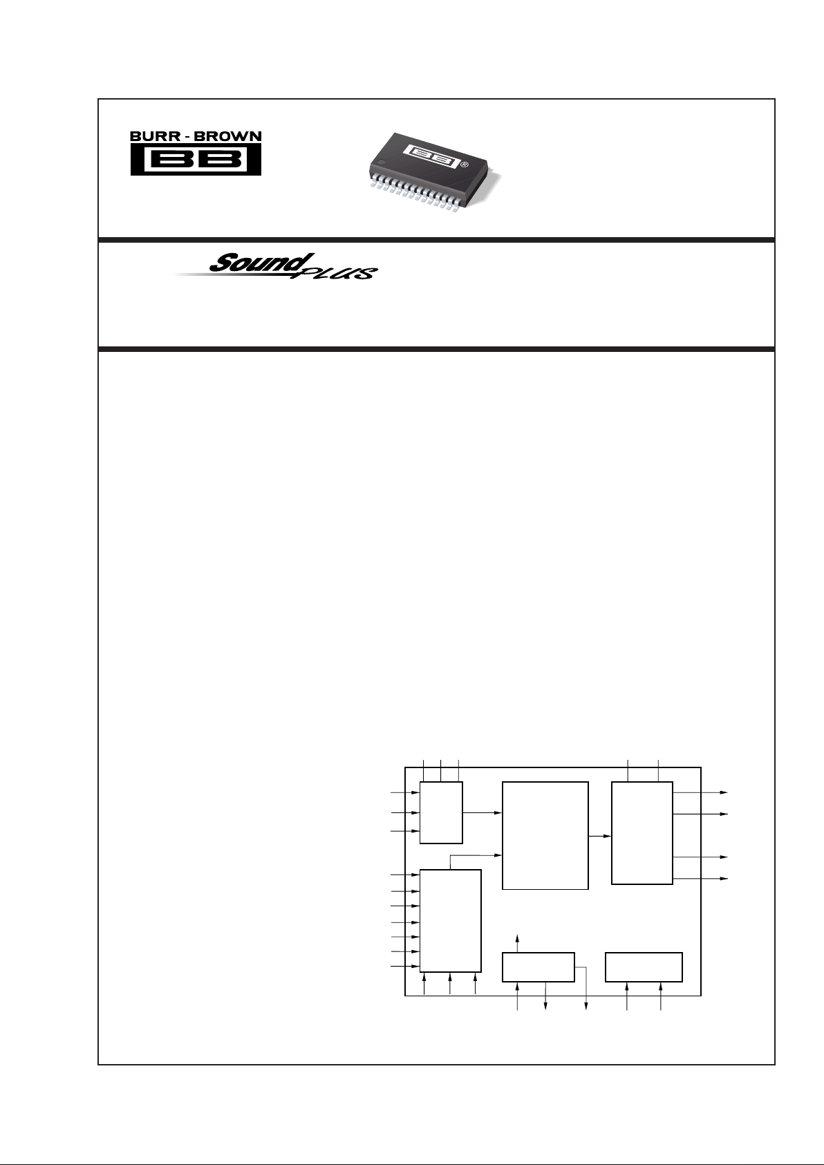
DF1704
Serial
Input
I/F
Mode
Control
I/F
8X Oversampling
Digital Filter with
Function
Controller
Crystal/OSC
XTI
SCK
XTO CLKO(SF0) (SF1) (SRO) V
DDVSS
Output I/F
BCKO
(I
2
S)
(IW1)
(IW0)
(OW1)
(OW0)
WCKO
DOL
DOR
MC/LRIP
MD/CKO
LRCIN
DIN
BCKIN
MODE
ML/RESV
(MUTE)
RST
(DEM)
Power Supply
International Airport Industrial Park • Mailing Address: PO Box 11400, Tucson, AZ 85734 • Street Address: 6730 S. Tucson Blvd., Tucson, AZ 85706 • Tel: (520) 746-1111
Twx: 910-952-1111 • Internet: http://www.burr-brown.com/ • Cable: BBRCORP • Telex: 066-6491 • FAX: (520) 889-1510 • Immediate Product Info: (800) 548-6132
®
2
DF1704
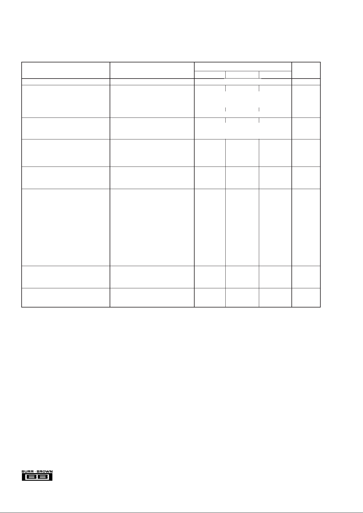
SPECIFICATIONS
All specifications at +25°C, VDD = +5V, unless otherwise noted.
DF1704E
PARAMETER CONDITIONS MIN TYP MAX UNITS
RESOLUTION 24 Bits
INPUT DATA FORMAT
Audio Data Interface Format Standard / Left-Justified /I2S
Audio Data Bit Length 16/20 /24 Selectable
Audio Data Format MSB-First, Two’s Binary Comp
Sampling Frequency (f
S
) 32 96 kHz
System Clock Frequency 256/384/512/768f
S
OUTPUT DATA FORMAT
Audio Data Interface Format Right-Justified
Audio Data Bit Length 16/20 /24 Selectable
Audio Data Format MSB-First, Binary Two’s Complement
DIGITAL INPUT/OUTPUT
Input Logic Level: V
IH
2.0 V
V
IL
0.8 V
Output Logic Level: V
OH
I
OH
= 2mA 4.5 V
V
OL
I
OL
= 4mA 0.5 V
CLKO AC CHARACTERISTICS
Rise Time (t
R
) 20% to 80% VDD, 10pF 4 ns
Fall Time (tF) 80% to 20% VDD, 10pF 3 ns
Duty Cycle 10pF Load 37 %
DIGITAL FILTER PERFORMANCE
Filter Characteristics 1 (Sharp Roll-Off)
Passband ±0.00005dB 0.454f
S
–3dB 0.493f
S
Stopband 0.546f
S
Passband Ripple ±0.00005 dB
Stopband Attenuation Stopband = 0.546f
S
–115 dB
Filter Characteristics 2 (Sharp Roll-Off)
Passband Ripple ±0.0001dB 0.254f
S
–3dB 0.460f
S
Stopband 0.732f
S
Passband Ripple ±0.0001 dB
Stopband Attenuation Stopband = 0.748f
S
–100 dB
Delay Time 45.125/f
S
sec
De-Emphasis Error ±0.003 dB
POWER SUPPLY REQUIREMENTS
Voltage Range V
DD
4.5 5 5.5 VDC
Supply Current: I
DD
20 30 mA
Power Dissipation 100 150 mW
TEMPERATURE RANGE
Operation –25 +85 °C
Storage –55 +100 °C
®
3 DF1704
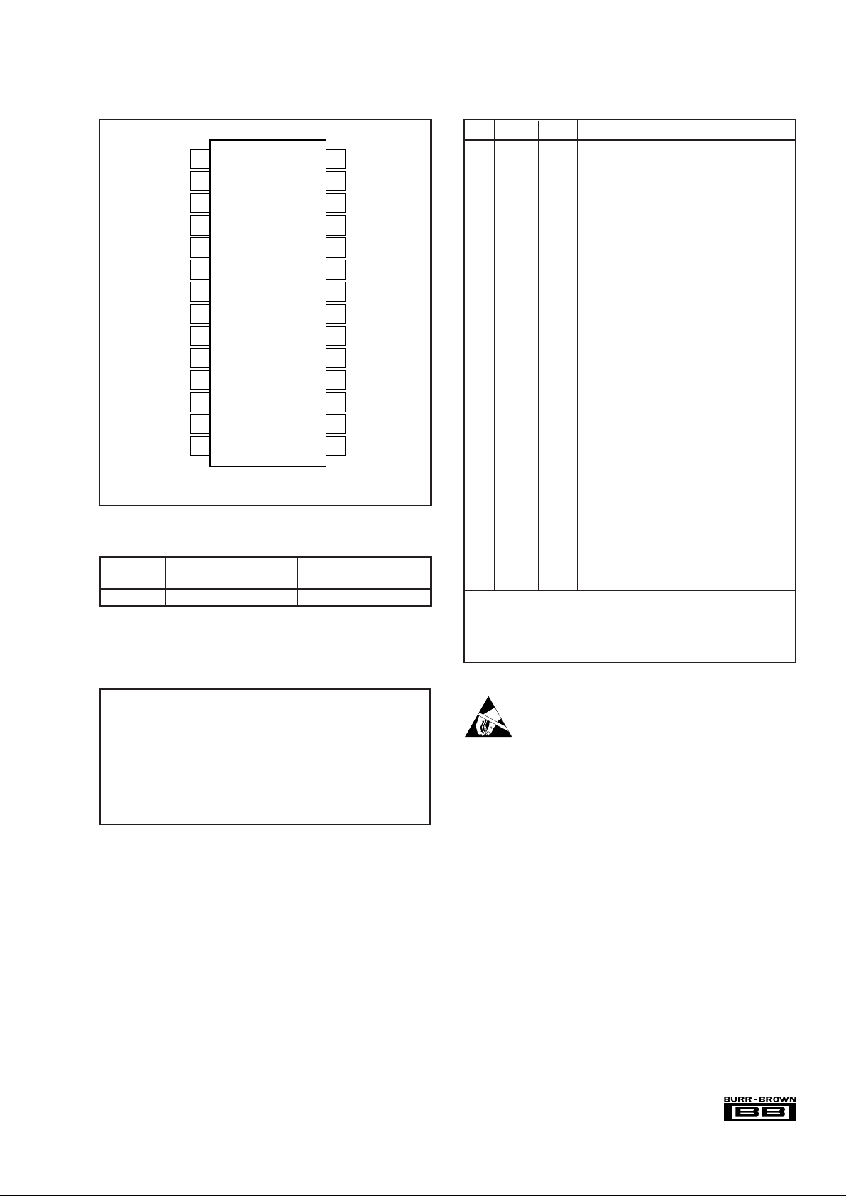
PIN NAME I/O DESCRIPTION
1 DIN IN Serial Audio Data Input
(3)
2 BCKIN IN Bit Clock Input for Serial Audio Data
(3)
3I
2
S IN Input Audio Data Format Selection
(2, 4)
4 IW0 IN Input Audio Data Word Selection
(2, 4)
5 IW1 IN Input Audio Data Word Selection
(2, 4)
6 XTI IN Oscillator Input / External Clock Input
7 XTO OUT Oscillator Output
8V
SS
— Digital Ground
9 CLKO OUT Buffered System Clock Output
10 MODE IN Mode Control Selection (H: Software, L: Hardware)
(1)
11 MD/CKO IN Control Data Input/Clock Output Frequency
Select
(1, 5)
12 MC/LRIP IN Control Data Clock/Polarity of LRCK Select
(1, 5)
13
ML/RESV
IN Control Data Latch/Reserved
(1, 5)
14 RST IN Reset. When this pin is LOW, the digital filter
is held in reset.
(1)
15 MUTE IN Mute Control
(1, 4)
16 DEM IN De-Emphasis Control
(2, 4)
17 SF0 IN Sampling Rate Select for De-emphasis
(2, 4)
18 SF1 IN Sampling Rate Select for De-emphasis
(2, 4)
19 OW0 IN Output Audio Data Word and Format Select
(2, 4)
20 OW1 IN Output Audio Data Word and Format Select
(2, 4)
21 NC — No Connection
22 V
DD
— Digital Power, +5V
23 DOR OUT Rch, Serial Audio Data Output
24 DOL OUT Lch, Serial Audio Data Output
25 WCKO OUT Word Clock for Serial Audio Data Output
26 BCKO OUT Bit Clock for Serial Audio Data Output
27 SRO IN Filter Response Select
(2, 4)
28 LRCIN IN L/R Clock Input (fS) for Serial Audio Data
(3)
NOTES: (1) Pins 10-15; Schmitt-Trigger input with pull-up resistor. (2) Pins
3-5, 16-20, 27; Schmitt-Trigger input with pull-down resister. (3) Pins 1, 2,
28; Schmitt-Trigger input. (4) Pins 3-5, 15-20, 27; these pins are invalid
when MODE (pin 10) is HIGH. (5) Pins 11-13; these pins have different
functions corresponding to MODE (pin 10), (HIGH/LOW).
PIN ASSIGNMENTSPIN CONFIGURATION
PACKAGE DRAWING
PRODUCT PACKAGE NUMBER
(1)
DF1704E 28-Lead SSOP 324
NOTE: (1) For detailed drawing and dimension table, please see end of data
sheet, or Appendix C of Burr-Brown IC Data Book.
PACKAGE INFORMATION
ELECTROSTATIC
DISCHARGE SENSITIVITY
This integrated circuit can be damaged by ESD. Burr-Brown
recommends that all integrated circuits be handled with
appropriate precautions. Failure to observe proper handling
and installation procedures can cause damage.
ESD damage can range from subtle performance degradation
to complete device failure. Precision integrated circuits may
be more susceptible to damage because very small parametric
changes could cause the device not to meet its published
specifications.
The information provided herein is believed to be reliable; however, BURR-BROWN assumes no responsibility for inaccuracies or omissions. BURR-BROWN assumes
no responsibility for the use of this information, and all use of such information shall be entirely at the user’s own risk. Prices and specifications are subject to change
without notice. No patent rights or licenses to any of the circuits described herein are implied or granted to any third party. BURR-BROWN does not authorize or warrant
any BURR-BROWN product for use in life support devices and/or systems.
Supply Voltage (V
DD
, VCC1, VCC2R, VCC2L)....................................+6.5V
Supply Voltage Differences................................................................. ±0.1
GND Voltage Differences.................................................................. ±0.1V
Digital Input Voltage................................................. –0.3V to (V
DD
+ 0.3V)
Input Current (any pins except power supplies) ............................. ±10mA
Power Dissipation .......................................................................... 300mW
Operating Temperature Range ......................................... –25°C to +85°C
Storage Temperature...................................................... –55°C to +125°C
Lead Temperature (soldering, 5s)................................................. +260°C
Package Temperature (reflow, 10s) .............................................. +235°C
ABSOLUTE MAXIMUM RATINGS
DIN
BCKIN
I
2
S
IW0
IW1
XTI
XTO
V
SS
CLKO
MODE
MD/CKO
MC/LRIP
ML/RESV
RST
LRCIN
SRO
BCKO
WCKO
DOL
DOR
V
DD
NC
OW1
OW0
SF1
SF0
DEM
MUTE
1
2
3
4
5
6
7
8
9
10
11
12
13
14
28
27
26
25
24
23
22
21
20
19
18
17
16
15
DF1704E
NC: No Connection
®
4
DF1704
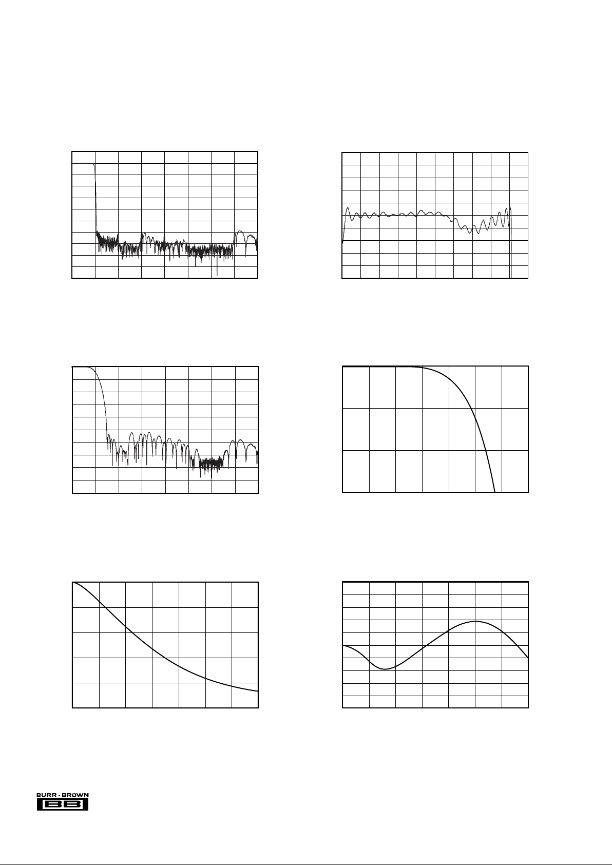
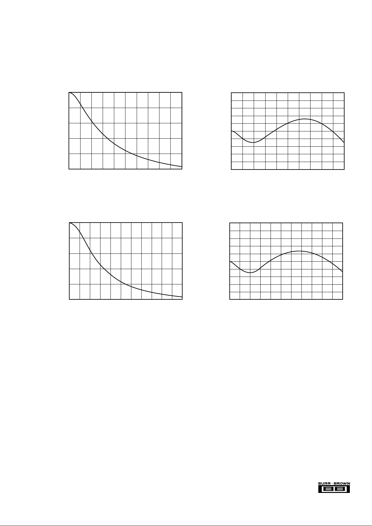
TYPICAL PERFORMANCE CURVES OF INTERNAL FIL TER
DIGITAL FILTER (DE-EMPHASIS OFF, fS = 44.1kHz)
DE-EMPHASIS AND DE-EMPHASIS ERROR
043.532.521.510.5
Frequency (f
S
)
20
0
–20
–40
–60
–80
–100
–120
–140
–160
–180
–200
FREQUENCY RESPONSE (Sharp Roll Off)
Attenuation (dB)
00.50.450.40.3 0.350.250.20.150.10.5
Frequency (f
S
)
0.0001
0.00008
0.00006
0.00004
0.00002
0
–0.00002
–0.00004
–0.00006
–0.00008
–0.0001
PASSBAND RIPPLE (Sharp Roll Off)
Attenuation (dB)
043.532.521.510.5
Frequency (f
S
)
0
–20
–40
–60
–80
–100
–120
–140
–160
–180
–200
FREQUENCY RESPONSE (Slow Roll Off)
Attenuation (dB)
0 0.1 0.2 0.3 0.4 0.5 0.70.6
Frequency (f
S
)
TRANSITION CHARACTERISTIC (Slow Roll Off)
0
–5
–10
–15
Attenuation (dB)
01412108642
Frequency ( f
S
)
0
–2
–4
–6
–8
–10
DE-EMPHASIS (f
S
= 32kHz)
Level (dB)
01412810642
Frequency (f
S
)
0.01
0.008
0.006
0.004
0.002
0
–0.002
–0.004
–0.006
–0.008
–0.01
DE-EMPHASIS ERROR (f
S
= 32kHz)
Error (dB)
®
5 DF1704
TYPICAL PERFORMANCE CURVES OF INTERNAL FIL TER
020181610 14128642
Frequency (f
S
)
0
–2
–4
–6
–8
–10
DE-EMPHASIS (f
S
= 44.1kHz)
Level (dB)
020181610 14128642
Frequency (f
S
)
DE-EMPHASIS ERROR (f
S
= 44.1kHz)
0.01
0.008
0.006
0.004
0.002
0
–0.002
–0.004
–0.006
–0.008
–0.01
Error (dB)
02220181610 14128642
Frequency (f
S
)
0
–2
–4
–6
–8
–10
DE-EMPHASIS (f
S
= 48kHz)
Level (dB)
02220181610 14128642
Frequency (f
S
)
DE-EMPHASIS ERROR (f
S
= 48kHz)
0.01
0.008
0.006
0.004
0.002
0
–0.002
–0.004
–0.006
–0.008
–0.01
Error (dB)
 Loading...