

Datasheet DAC811KU, DAC811KP, DAC811JU-1K, DAC811JU, DAC811JP Datasheet (Burr Brown Corporation)
...
®
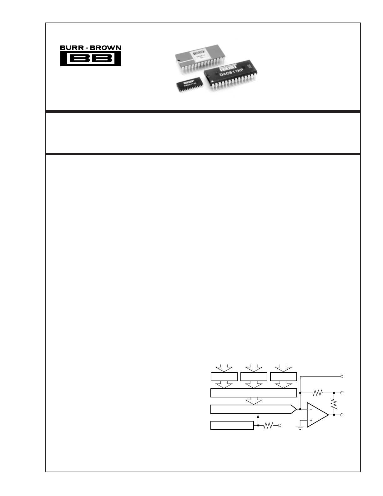
BPO
V
OUT
D/A Latch
Input Latch
4 MSBs
Input Latch Input Latch
4 LSBs
12-Bit D/A Converter
Voltage Reference
10V
R
F
S
J
R
F
R
BPO
For most current data sheet and other product
information, visit www.burr-brown.com
Microprocessor-Compatible
12-BIT DIGITAL-TO-ANALOG CONVERTER
DAC811
FEATURES
● SINGLE INTEGRATED CIRCUIT CHIP
● MICROCOMPUTER INTERFACE:
DOUBLE-BUFFERED LATCH
● VOLTAGE OUTPUT: ±10V, ±5V, +10V
● MONOTONICITY GUARANTEED OVER
TEMPERATURE
● ±1/2LSB MAXIMUM NONLINEARITY OVER
TEMPERATURE
● GUARANTEED SPECIFICATIONS AT ±12V
AND ±15V SUPPLIES
● TTL/5V CMOS-COMPATIBLE LOGIC
INPUTS
Input gating logic is designed so that loading the last
nibble or byte of data can be accomplished simultaneously with the transfer of data (previously stored in
adjacent latches) from adjacent input latches to the
D/A latch. This feature avoids spurious analog output
values while using an interface technique that saves
computer instructions.
The DAC811 is laser trimmed at the wafer level and
is specified to ±1/4LSB maximum linearity error (B,
K, and S grades) at 25°C and ±1/2LSB maximum over
the temperature range. All grades are guaranteed monotonic over the specification temperature range.
The DAC811 is available in six performance grades
and three package types. DAC811J and K are specified over the temperature ranges of 0°C to +70°C;
DAC811A and B are specified over –25°C to +85°C;
DAC811R and S are specified over –55°C to +125°C.
DESCRIPTION
The DAC811 is a complete, single-chip integratedcircuit, microprocessor-compatible, 12-bit digital-toanalog converter. The chip combines a precision voltage reference, microcomputer interface logic, and
DAC811J and K are packaged in a reliable 28-pin
plastic DIP or plastic SOIC package, while DAC811A,
B, R and S are available in a 28-pin 0.6" wide dualinline hermetically sealed ceramic side-brazed package (H package).
double-buffered latch, in a 12-bit D/A converter with
a voltage output amplifier. Fast current switches and a
laser-trimmed thin-film resistor network provide a
highly accurate and fast D/A converter.
Microcomputer interfacing is facilitated by a doublebuffered latch. The input latch is divided into three
4-bit nibbles to permit interfacing to 4-, 8-, 12-, or
16-bit buses and to handle right-or left-justified data.
The 12-bit data in the input latches is transferred to the
D/A latch to hold the output value.
International Airport Industrial Park • Mailing Address: PO Box 11400, Tucson, AZ 85734 • Street Address: 6730 S. Tucson Blvd., Tucson, AZ 85706 • Tel: (520) 746-1111
Twx: 910-952-1111 • Internet: http://www.burr-brown.com/ • Cable: BBRCORP • Telex: 066-6491 • FAX: (520) 889-1510 • Immediate Product Info: (800) 548-6132
© 1983 Burr-Brown Corporation PDS-503K Printed in U.S.A. January, 2000
1
DAC811
®
SPECIFICATIONS
At TA = +25°C. ±VCC = 12V or 15V, unless otherwise noted.
DAC811AH, JP, JU DAC811BH, KP, KU
DAC811RH DAC811SH
PARAMETER MIN TYP MAX MIN TYP MAX MIN TYP MAX MIN TYP MAX UNITS
DIGITAL INPUT
Resolution 12 ✻✻✻Bits
(1)
Codes
Digital Inputs Over Temperature Range
V
IH
V
IL
I
, VI = +2.7V +10 ✻✻✻µA
IH
I
, VI = +0.4V ±20 ✻✻✻µA
IL
Digital Interface Timing Over Temperature Range
(2)
USB, BOB
✻✻✻
+2 +15 ✻✻✻✻✻✻VDC
0 +0.8 ✻✻✻✻✻✻VDC
tWP, WR Pulse Width 50 ✻✻✻ ns
t
1, NX and LDAC Valid to End of WR 50 ✻✻✻
AW
, Data Valid to End of WR 80 ✻✻✻ ns
DW
t
, Data Valid Hold Time 0 ✻ +10 ✻ ns
DH
nst
ACCURACY
Linearity Error ±1/4 ±1/2 ±1/8 ±1/4 ±1/4 ±1/2 ±1/8 ±1/4 LSB
Differential Linearity Error ±1/2 ±3/4 ±1/4 ±1/2 ±1/2 ±3/4 ±1/4 ±1/2 LSB
Gain Error
Offset Error
(3)
(3, 4)
±0.1 ±0.2 ✻✻ ✻✻ ✻✻ %
±0.05 ±0.15 ✻✻ ✻✻ ✻✻ % of FSR
(5)
Monotonicity Guaranteed ✻✻✻
Power Supply Sensitivity: +V
–V
CC
V
DD
CC
±0.001 ±0.003 ✻✻ ✻✻ ✻ ✻% of FSR/%V
±0.002 ±0.006 ✻✻ ✻✻ ✻ ✻% of FSR/%V
±0.0005 ±0.0015 ✻✻ ✻✻ ✻✻% of FSR/%V
CC
CC
DD
DRIFT (Over Specification Temperature Range)
Gain ±10 ±30 ±10 ±20 ±15 ±30 ±15 ±30 ppm/°C
Unipolar Offset ±5 ±10 ±5 ±7 ±5 ±10 ±5 ±7 ppm of FSR/°C
Bipolar Zero ±5 ±10 ±5 ±7 ±5 ±10 ±5 ±7 ppm of FSR/°C
Linearity Error Over Temperature Range ±1/2 ±3/4 ±1/4 ±1/2 ±1/2 ±3/4 ±1/4 ±1/2 LSB
Monotonicity Over Temperature Range Guaranteed ✻✻✻
SETTLING TIME
(6)
(to within ±0.01% of FSR of Final Value; 2kΩ load)
For Full Scale Range Change, 20V Range 3 4 ✻✻ ✻✻ ✻✻ µs
10V Range 3 4 ✻✻ ✻✻ ✻✻ µs
For 1LSB Change at Major Carry
Slew Rate
(6)
ANALOG OUTPUT
Voltage Range (±V
Bipolar ±5, ±10 ✻✻✻V
= 15V)
CC
(7)
1 ✻✻✻µs
812 ✻✻ ✻✻ ✻✻ V/µs
(8)
: Unipolar 0 to +10 ✻✻✻V
Output Current ±5 ✻✻✻ mA
Output Impedance (at DC) 0.2 ✻✻✻Ω
Short Circuit to Common Duration Indefinite ✻✻✻
REFERENCE VOLTAGE
Voltage +6.2 +6.3 +6.4 ✻✻✻✻✻✻✻✻✻ V
Source Current Available for External Loads +2 ✻✻✻ mA
Temperature Coefficient ±10 ±30 ±10 ±20 ±10 ±30 ±10 ±20 ppm/°C
Short Circuit to Common Duration Indefinite ✻✻✻
POWER SUPPLY REQUIREMENTS
Voltage: +V
–V
V
DD
Current (no load): +V
–V
V
DD
Potential at DCOM with Respect to ACOM
CC
CC
CC
CC
+11.4 +15 +16.5 ✻✻✻✻✻✻✻✻✻ VDC
–11.4 –15 –16.5 ✻✻✻✻✻✻✻✻✻ VDC
+4.5 +5 +5.5 ✻✻✻✻✻✻✻✻✻ VDC
+16 +25 ✻✻ ✻✻ ✻✻ mA
–23 –35 ✻✻ ✻✻ ✻✻ mA
(9)
+8 +15 ✻✻ ✻✻ ✻✻ mA
±0.5 ✻✻✻V
Power Dissipation 625 800 ✻✻ ✻✻ ✻✻ mW
TEMPERATURE RANGE
Specification: J, K 0 +70 ✻✻✻✻✻✻°C
A, B –25 +85 ✻✻✻✻✻✻°C
R, S –65 +150 ✻✻✻✻✻✻°C
–55 +125 ✻✻°C
Storage: J, K –60 +100 ✻✻✻✻✻✻°C
A, B, R, S –65 +150 ✻✻✻✻✻✻°C
✻ Specification same as DAC811AH.
NOTES: (1) USB = unipolar straight binary; BOB = bipolar offset binary. (2) TTL, LSTTL and 54/74 HC compatible. (3) Adjustable to zero with external trim
potentiometer. (4) Error at input code 000
represents the 3σ limit. Not 100% tested for this parameter. (7) At the major carry, 7FF
output swing is ±13.5V. Output swing for ±11.4V supplies is at least –8V to +8V. (9) The maximum voltage at which ACOM and DCOM may be separated without
for both unipolar and bipolar ranges. (5) FSR means full scale range and is 20V for the ±10V range. (6) Maximum
16
to 80016 and 80016 to 7FF16. (8) Minimum supply voltage required for ±10V
16
affecting accuracy specifications.
®
DAC811
2
PIN DESCRIPTIONS
PIN
NAME FUNCTION
1+V
DD
2 WR Write, command signal to load latches. Logic low
3 LDAC Load D/A converter, enables WR to load the D/A
4N
A
5N
B
6N
C
7D
11
8D
10
9D
9
10 D
8
11 D
7
12 D
6
13 D
5
14 D
4
15 DCOM Digital common, V
16 D
0
17 D
1
18 D
2
19 D
3
20 +V
CC
21 –V
CC
22 Gain Adj To externally adjust gain.
23 ACOM Analog common, ±V
24 V
OUT
25 10V Range Connect to pin 24 for 10V range.
26 SJ Summing junction of output amplifier.
27 BPO Bipolar offset. Connect to pin 26 for bipolar
28 Ref Out 6.3V reference output.
Logic supply, +5V.
loads latches.
latch. Logic low enables.
Nibble A, enables WR to load input latch A (the
most significant nibble). Logic low enables.
Nibble B, enables WR to load input latch B. Logic
low enables.
Nibble C, enables WR to load input latch C (the
least significant nibble). Logic low enables.
Data bit 12, MSB, positive true.
Data bit 11.
Data bit 10.
Data bit 9.
Data bit 8.
Data bit 7.
Data bit 6.
Data bit 5.
supply return.
Data bit 1, LSB.
Data bit 2.
Data bit 3.
Data bit 4.
Analog supply input, +15V or +12V.
Analog supply input, –15V or –12V.
D/A converter voltage output.
operation.
DD
supply return.
CC
ABSOLUTE MAXIMUM RATINGS
+V
................................................................................................................................ 0 to +18V
CC
–V
to ACOM .......................................................................... 0 to –18V
CC
V
to DCOM .............................................................................. 0 to +7V
DD
V
to ACOM ......................................................................................±7V
DD
ACOM to DCOM .................................................................................. ±7V
Digital Inputs (Pins 2–14, 16–19) to DCOM ......................–0.4V to +18V
External Voltage Applied to 10V Range Resistor ............................ ±12V
Ref Out ............................................................. Indefinite Short to ACOM
External Voltage Applied to DAC Output ................................ –5V to +5V
Power Dissipation ........................................................................ 1000mW
Lead Temperature (soldering, 10s) ............................................... +300°C
Max Junction Temperature ............................................................ +165°C
Thermal Resistance,
Ceramic DIP .................................................................................. 65°C/W
NOTE: Stresses above those listed above may cause permanent damage to
the device. Exposure to absolute maximum conditions for extended periods
may affect device reliability.
θ
: Plastic DIP and SOIC ....................... 100°C/W
J-A
ELECTROSTATIC
DISCHARGE SENSITIVITY
This integrated circuit can be damaged by ESD. Burr-Brown
recommends that all integrated circuits be handled with
appropriate precautions. Failure to observe proper handling
and installation procedures can cause damage.
ESD damage can range from subtle performance degradation
to complete device failure. Precision integrated circuits may
be more susceptible to damage because very small parametric
changes could cause the device not to meet its published
specifications.
PACKAGE/ORDERING INFORMATION
MINIMUM
RELATIVE DIFFERENTIAL PACKAGE SPECIFICATION
PRODUCT (LSB) (LSB) PACKAGE NUMBER RANGE NUMBER
ACCURACY LINEARITY DRAWING TEMPERATURE ORDERING TRANSPORT
DAC811AH ±1/2 LSB 3/4 CerDIP-28 149 –25°C to +85°C DAC811AH Rails
DAC811JP ±1/2 LSB 3/4 DIP-28 215 0°C to +70°C DAC811JP Rails
DAC811JU ±1/2 LSB 3/4 SOIC-28 217 0°C to +70°C DAC811JU Rails
"" """ "DAC811JU/1K Tape and Reel
DAC811KP ±1/4 LSB 1/2 DIP-28 215 0°C to +70°C DAC811KP Rails
DAC811KU ±1/4 LSB 1/2 SOIC-28 217 0°C to +70°C DAC811KU Rails
NOTE: (1) Models with a slash (/) are available only in Tape and Reel in the quantities indicated (e.g., /1K indicates 1000 devices per reel). Ordering 1000 pieces
of “DAC811JU/1K” will get a single 1000-piece Tape and Reel.
The information provided herein is believed to be reliable; however, BURR-BROWN assumes no responsibility for inaccuracies or omissions. BURR-BROWN assumes
no responsibility for the use of this information, and all use of such information shall be entirely at the user’s own risk. Prices and specifications are subject to change
without notice. No patent rights or licenses to any of the circuits described herein are implied or granted to any third party. BURR-BROWN does not authorize or warrant
any BURR-BROWN product for use in life support devices and/or systems.
(1)
MEDIA
®
3
DAC811
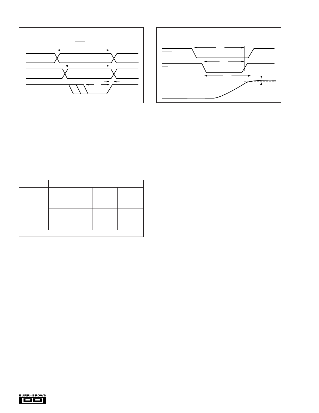
TIMING DIAGRAMS
Write Cycle #1
Load first rank from Data Bus: LDAC = 1
t
AW
N
, NB, N
C
A
t
DW
DB11–DB
0
t
DH
WR
t
WP
DISCUSSION OF
SPECIFICATIONS
INPUT CODES
The DAC811 accepts positive-true binary input codes.
DAC811 may be connected by the user for any one of the
following codes: USB (unipolar straight binary), BOB (bipolar offset binary) or, using an external inverter on the
MSB line, BTC (binary two’s complement). See Table I.
DIGITAL INPUT
Unipolar Bipolar Binary
MSB LSB
↓↓
111111111111 + Full Scale + Full Scale –1LSB
100000000000 + 1/2 Full Scale Zero – Full Scale
011111111111
000000000000 Zero – Full Scale Zero
NOTE: (1) Invert MSB of the BOB code with external inverter to obtain BTC code.
Straight Offset Two’s
Binary Binary
+ 1/2 Full Scale – 1LSB
TABLE I. Digital Input Codes.
LINEARITY ERROR
Linearity error as used in D/A converter specifications by
Burr-Brown is the deviation of the analog output from a
straight line drawn between the end points (inputs all 1s and
all 0s). The DAC811 linearity error is specified at ±1/4LSB
(max) at +25°C for B and K grades, and ±1/2LSB (max) for
A, J, and R grades.
DIFFERENTIAL LINEARITY ERROR
Differential linearity error (DLE) is the deviation from a
1LSB output change from one adjacent state to the next. A
DLE specification of 1/2LSB means that the output step size
can range from 1/2LSB to 3/2LSB when the input changes
from one state to the next. Monotonicity requires that DLE
be less than 1LSB over the temperature range of interest.
MONOTONICITY
A D/A converter is monotonic if the output either increases
or remains the same for increasing digital inputs. All grades
of DAC811 are monotonic over their specification temperature range.
®
DAC811
ANALOG OUTPUT
USB BOB BTC
Complement
–1LSB + Full Scale
(1)
Write Cycle #2
Load second rank from first rank: NA, N , NCB= 1
t
AW
LDAC
t
WP
WR
t
SET
±1/2LSB
DRIFT
Gain drift is a measure of the change in the full scale range
(FSR) output over the specification temperature range. Drift is
expressed in parts per million per degree centigrade
(ppm/°C). Gain drift is established by testing the full scale
range value (e.g., +FS minus –FS) at high temperature, +25°C,
and low temperature, calculating the error with respect to the
+25°C value, and dividing by the temperature change.
Unipolar offset drift is a measure of the change in output
with all 0s on the input over the specification temperature
range. Offset is measured at high temperature, +25°C, and
low temperature. The offset drift is the maximum change in
offset referred to the +25°C value, divided by the temperature change. It is expressed in parts per million of full scale
range per degree centigrade (ppm of FSR/°C).
Bipolar zero drift is measured at a digital input of 80016, the
code that gives zero volts output for bipolar operation.
SETTLING TIME
Settling time is the total time (including slew time) for the
output to settle within an error band around its final value
after a change in input. Three settling times are specified to
±0.01% of full scale range (FSR): two for maximum full
scale range changes of 20V and 10V, and one for a 1LSB
change. The 1LSB change is measured at the major carry
(7FF16 to 80016 and 80016 to 7FF16), the input transition at
which worst-case settling time occurs.
REFERENCE SUPPLY
DAC811 contains an on-chip 6.3V reference. This voltage
(pin 28) has a tolerance of ±0.1V. The reference output may
be used to drive external loads, sourcing at least 2mA. This
current should be constant for best performance of the D/A
converter.
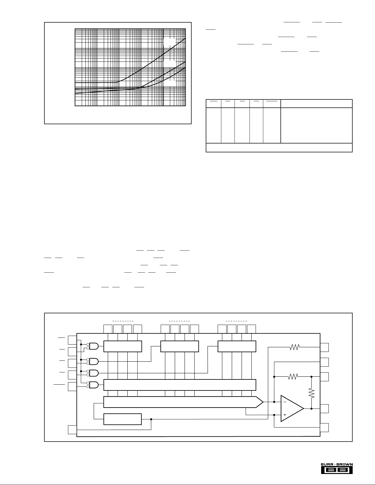
POWER SUPPLY SENSITIVITY
Power supply sensitivity is a measure of the effect of a
power supply change on the D/A converter output. It is
defined as a percent of FSR output change per percent of
change in either the positive, negative, or logic supply
voltages about the nominal voltages. Figure 1 shows typical
power supply rejection versus power supply ripple frequency.
4
1
–V
+V
CC
V
DD
CC
M1
0.1
0.01
0.001
Percent of FSR per Percent of
Change of Power Supply Voltage
0.0001
10 100 1k 10k 100k
Frequency (Hz)
FIGURE 1. Power Supply Rejection vs Power Supply Ripple
Frequency.
OPERA TION
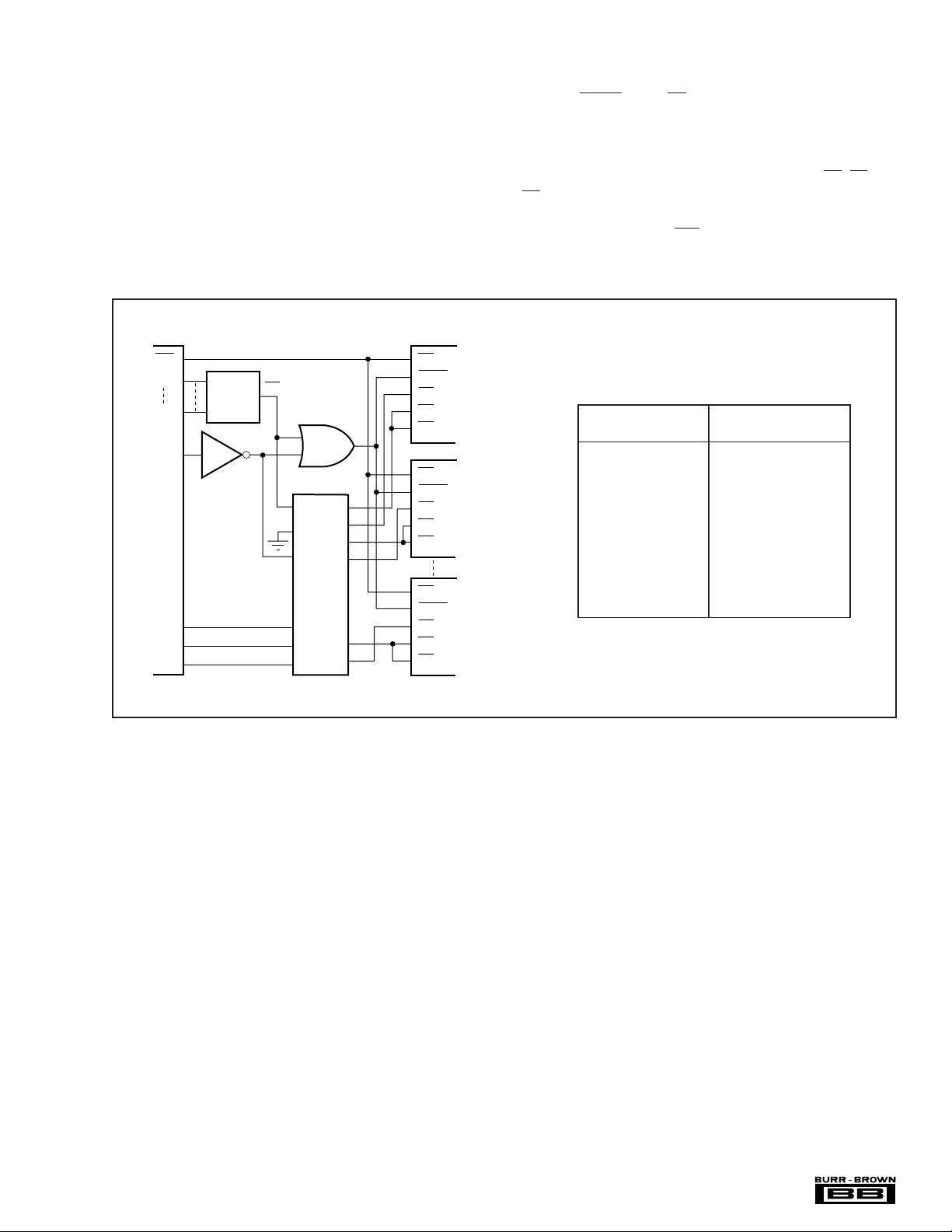
DAC811 is a complete single IC chip 12-bit D/A converter.
The chip contains a 12-bit D/A converter, voltage reference,
output amplifier, and microcomputer-compatible input logic
as shown in Figure 2.
The D/A latch is controlled by LDAC and WR. LDAC and
WR are internally NORed so that the latches transmit data to
the D/A switches when both LDAC and WR are at logic 0.
When either LDAC or WR are at logic 1, the data is latched
in the D/A latch and held until LDAC and WR go to logic 0.
All latches are level-triggered. Data present when the control signals are logic 0 will enter the latch. When any one of
the control signals returns to logic 1, the data is latched.
Table II is a truth table for all latches.
WR
NANBNCLDAC
1 X X X X No operation
0 0 1 1 1 Enables input latch 4MSBs
0 1 0 1 1 Enables input latch 4 middle bits
0 1 1 0 1 Enables input latch 4LSBs
0111 0
0 0 0 0 0 Makes all latches transparent
“X” = Don’t care.
OPERATION
Loads D/A latch from input latches
TABLE II. DAC813 Interface Logic Truth Table.
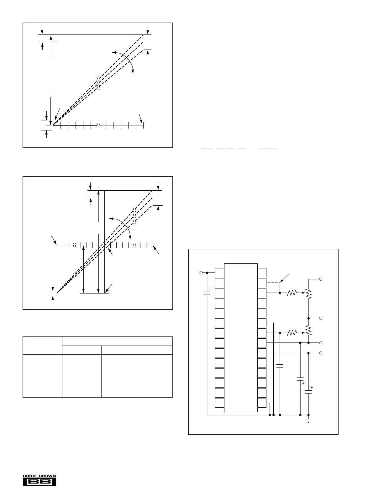
GAIN AND OFFSET ADJUSTMENTS
Figures 3 and 4 illustrate the relationship of offset and gain
adjustments to unipolar and bipolar D/A converter output.
INTERFACE LOGIC
Input latches A, B, and C hold data temporarily while a
complete 12-bit word is assembled before loading into the
D/A register. This double-buffered organization prevents the
generation of spurious analog output values. Each register is
independently addressable.
These input latches are controlled by NA, NB, NC, and WR.
NA, NB, and NC are internally NORed with WR so that the
input latches transmit data when both NA (or NB, NC) and
WR are at logic 0. When either NA, (NB, NC) or WR go to
logic 1, the input data is latched into the input registers and
held until both NA (or NB, NC) and WR go to logic 0.
D11 D8 D7
MSB LSB
7 8 9 10 11 12 13 14 19 18 17 16
N
N
N
LDAC
Ref Out
2WR
4
A
5
B
6
C
3
28
4-Bit Latch, A
Reference
4-Bit Latch, B 4-Bit Latch, C
12-Bit D/A Latch
12-Bit D/A Converter
OFFSET ADJUSTMENT
For unipolar (USB) configurations, apply the digital input
code that should produce zero voltage output, and adjust the
offset potentiometer for zero output. For bipolar (BOB,
BTC) configurations, apply the digital input code that should
produce the maximum negative output voltage and adjust
the offset potentiometer for minus full scale voltage. Example: If the full scale range is connected for 20V, the
maximum negative output voltage is –10V. See Table III for
corresponding codes.
D4 D3
D0
R
BPO
R
F
R
F
BPO
27
SJ
26
10V
25
Range
V
24
OUT
ACOM
23
FIGURE 2. DAC811 Block Diagram.
®
5
DAC811
1LSB
+ Full Scale
Range of
Gain Adjust
±12V OPERATION
The DAC811 is fully specified for operation on ±12V power
supplies. However, in order for the output to swing to ±10V,
the power supplies must be ±13.5V or greater. When operating with ±12VB supplies, the output swing should be
restricted to ±8V in order to meet specifications.
Gain Adjust
Analog Output
Full Scale Range
Range of
Offset Adj.
Offset Adjust Translates the Line
All Bits
Logic 0
Digital Input
Rotates the Line
All Bits
Logic 1
FIGURE 3. Relationship of Offset and Gain Adjustments
for a Unipolar D/A Converter.
+ Full Scale
1LSB
Range of
All Bits
Logic 0
Analog Output
Range of
Offset Adjust
Offset Adj.
Translates
the Line
≈ ±0.4%
Bipolar V
Offset
Full Scale
Range
MSB on All
Others Off
– Full Scale
Digital Input
Gain Adjust
Gain Adjust
Rotates the Line
All Bits
Logic 1
FIGURE 4. Relationship of Offset and Gain Adjustments
for a Bipolar D/A Converter.
ANALOG OUTPUT
DIGITAL INPUT 0 to +10V
MSB LSB
↓↓
111111111111 +9.9976V +4.9976V +9.9951V
100000000000 +5V 0V 0V
011111111111 +4.9976V –0.0024V –0.0049V
000000000000 0V –5V –10V
LSB 2.4mV 2.44mV 4.88mV
±5V ±10V
TABLE III. Digital Input/Analog Output.
LOGIC INPUT COMPATIBILITY
The DAC811 digital inputs are TTL, LSTTL, and 54/74HC
CMOS-compatible over the operating range of VDD. The
input switching threshold remains at the TLL threshold over
the supply range.
The logic input current over temperature is low enough to
permit driving the DAC811 directly from the outputs of
4000B and 54/74C CMOS devices.
Resistors of 47Ω should be placed in series with D0 through
D11, WR, NA, NB, NC and LDAC if edges are <10ns or if
the logic input is driven below ground by undershoot.
INSTALLATION
POWER SUPPLY CONNECTIONS
For optimum performance and noise rejection, power supply
decoupling capacitors should be added as shown in Figure 5.
These capacitors (1µF tantalum recommended) should be
located close to the DAC811.
Connect for
V
DD
1µF
1
2
3
4
5
6
7
8
9
10
11
12
13
14
V
DD
Summing
Junction
Gain Adjust
BPO
V
OUT
ACOM
–V
CC
+V
CC
DCOM
28
27
26
25
24
23
22
21
20
19
18
17
16
15
Bipolar Operation
1MΩ
3.9MΩ
0.0022µF
1µF
10k to
100k
10k to
100k
1µF
–V
CC
Ω
Ω
+V
CC
Ω
Ω
–V
CC
+V
CC
GAIN ADJUSTMENT
For either unipolar or bipolar configurations, apply the
digital input that should give the maximum positive voltage
output. Adjust the gain potentiometer for this positive full
scale voltage. See Table III for positive full scale voltages.
®
DAC811
FIGURE 5. Power Supply, Gain, and Offset Potentiometer
Connections.
6
DAC811 features separate digital and analog power supply
returns to permit optimum connections for low noise and
high speed performance. The analog common (pin 23) and
digital common (pin 15) should be connected together at one
point. Separate returns minimize current flow in low level
signal paths if properly connected. Logic return currents are
not added into the analog signal return path. A ±0.5V
difference between ACOM and DCOM is permitted for
specified operation. High frequency noise on DCOM with
respect to ACOM may permit noise to be coupled through to
the analog output; therefore, some caution is required in
applying these common connections.
The Analog Common is the high quality return for the D/A
converter and should be connected directly to the analog
reference point of the system. The load driven by the output
amplifier should be returned to the Analog Common.
EXTERNAL OFFSET AND GAIN ADJUSTMENT
Offset and Gain may be trimmed by installing external
Offset and Gain potentiometers. Connect these potentiometers as shown in Figure 5. TCR of the potentiometers
should be 100ppm/°C or less. The 1MΩ and 3.9MΩ resistors (20% carbon or better) should be located close to the
DAC811 to prevent noise pickup. If it is not convenient to
use these high value resistors, an equivalent “T” network, as
shown in Figure 6, may be substituted in each case. The
Gain Adjust (pin 22) is a high impedance point and a
0.001µF to 0.01µF ceramic capacitor should be connected
from this pin to Analog Common to reduce noise pickup in
all applications, including those not employing external gain
adjustment. Excessive capacitance on the Gain Adjust or
Offset Adjust pin may affect slew rate and settling time.
1MΩ
3.9MΩ
100kΩ 100kΩ
12kΩ
180kΩ 180kΩ
10kΩ
From Voltage
Reference
From D/A
Converter
5.36kΩ
4.26kΩ
4.26kΩ
Bipolar Offset
27
26
Summing Junction
10V Range
25
V
24
OUT
23
Analog Common
FIGURE 7. Output Amplifier Voltage Range Scaling Circuit.
OUTPUT DIGITAL CONNECT CONNECT
RANGE INPUT CODES PIN 25 TO PIN 27 TO
0 to +10V USB 24 23
±5 BOB or BTC 24 26
±10V BOB or BTC NC 26
TABLE IV. Output Range Connections.
APPLICATIONS
MICROCOMPUTER BUS INTERFACING
The DAC811 interface logic allows easy interface to microcomputer bus structures. The control signal WR is derived
from external device select logic and the I/O Write or
Memory Write (depending upon the system design) signals
from the microcomputer.
The latch enable lines NA, NB, NC and LDAC determine
which of the latches are enabled. It is permissible to enable
two or more latches simultaneously, as shown in some of the
following examples.
The double-buffered latch permits data to be loaded into the
input latches of several DAC811s and later strobed into the
D/A latch of all D/As, simultaneously updating all analog
outputs. All the interface schemes shown below use a base
address decoder. If blocks of memory are used, the base
address decoder can be simplified or eliminated altogether.
For instance, if half the memory space is unused, address
line A15 of the microcomputer can be used as the chip select
control.
FIGURE 6. Equivalent Resistances.
OUTPUT RANGE CONNECTIONS
Internal scaling resistors provided in the DAC811 may be
connected to produce bipolar output voltage ranges of ±10V
and ±5V or a unipolar output voltage range of 0 to +10V.
The 20V range (±10V bipolar range) is internally connected.
Refer to Figure 7. Connections for the output ranges are
listed in Table IV.
4-BIT INTERFACE
An interface to a 4-bit microcomputer is shown in Figure 8.
Each DAC811 occupies four address locations. A 74LS139
provides the two-to-four decoder and selects it with the base
address. Memory Write (WR) of the microcomputer is
connected directly to the WR pin of the DAC811. An 8205
decoder is an alternative to the 74LS139.
7
DAC811
®
8-BIT INTERFACE
The control logic of DAC811 permits interfacing to rightjustified data formats, as illustrated in Figure 9. When a
12-bit D/A converter is loaded from an 8-bit bus, two bytes
of data are required. Figures 10 and 11 show an addressing
scheme for right-justified and left-justified data respectively.
The base address is decoded from the high-order address
bits. A0 and A1 address the appropriate latches. Note that
adjacent addresses are used. For the right-justified case,
X1016 loads the 8LSBs, and X0116 loads the 4MSBs and
simultaneously transfers input latch data to the D/A latch.
Addresses X0016 and X1116 are not used.
Left-justified data is handled in a similar manner, shown in
Figure 11. The DAC811 still occupies two adjacent locations in the microcomputer's memory map.
D0
16
D4
7
6
5
4
CS
(Chip
Select)
14
D8
10
D1
17
D5
13
D9
9
D2
18
D6
12
D10
8
D3
19
D7
11
D11
7
2
WR
LDAC
3
N
4
N
5
N
6
DAC811
A
B
C
DB0
DB1
DB2
DB3
Microcomputer
WR
A
N
A
2
A
1
A
0
Base
Address
Decoder
1
EN
3
A
1
2
A
0
1/2
74LS139
Y
3
Y
2
Y
1
Y
0
FIGURE 8. Addressing and Control for 4-Bit Microcom-
puter Interface.
X X X X D11 D10 D9 D8 D7 D6 D5 D4 D3 D2 D1 D0
a. Right-Justified
D11 D10 D9 D8 D7 D6 D5 D4 D3 D2 D1 D0
b. Left-Justified
XXXX
DB0
DB1
DB2
DB3
DB4
DB5
DB6
DB7
Microcomputer
WR
A
15
A
2
A
1
A
0
Base
Address
Decoder
CS
16
10
17
18
19
14
13
12
11
FIGURE 10. Right-Justified Data Bus Interface.
DB0
DB1
DB2
DB3
DB4
DB5
DB6
DB7
Microcomputer
WR
A
15
A
2
A
1
A
0
Base
Address
Decoder
CS
14
13
12
11
10
16
17
18
19
D0
D8
D1
D9
9
D2
D10
8
D3
D11
7
D4
D5
D6
DAC811
D7
2
WR
LDAC
3
N
4
A
N
5
B
N
6
C
D4
D5
D6
D7
D8
D0
D9
9
D1
D10
8
D2
D11
7
2
3
4
5
6
D3
WR
LDAC
N
A
N
B
N
C
DAC811
FIGURE 9. 12-Bit Data Format for 8-Bit Systems.
®
DAC811
FIGURE 11. Left-Justified Data Bus Interface.
8
INTERFACING MULTIPLE DAC811s
IN 8-BIT SYSTEMS
Many applications, such as automatic test systems, require
that the outputs of several D/A converters be updated simultaneously. The interface shown in Figure 12 uses a 74LS138
decoder to decode a set of eight adjacent addresses, to load
the input latches of four DAC811s. The example shows a
right-justified data format.
A ninth address using A3 causes all DAC811s to be updated
simultaneously. If a particular DAC811 is always loaded
last—for instance, D/A #4—A3 is not needed, thus saving
eight address spaces for other uses. Incorporate A3 into the
base address decoder, remove the inverter, connect the
common LDAC line to NC of D/A #4, and connect D1 of the
74LS138 to +5V.
12- AND 16-BIT MICROCOMPUTER INTERFACE
For this application, the input latch enable lines, NA, NB and
NC, are tied low, causing the latches to be transparent. The
D/A latch, and therefore DAC811, is selected by the address
decoder and strobed by WR.
WR
A
15
A
4
A
3
Microcomputer
A
2
A
1
A
0
Base
Address
Decoder
CS
4
5
6
3
2
1
74LS138
G
2A
G
2B
G
1
C
B
A
Y0
Y1
Y2
Y3
Y4
Y5
Y6
Y7
15
14
13
12
11
10
9
7
WR
LDAC
N
C
N
B
N
A
WR
LDAC
N
C
N
B
N
A
WR
LDAC
N
C
N
B
N
A
DAC811
(1)
DAC811
(2)
DAC811
(4)
FIGURE 12. Interfacing Multiple DAC811s to an 8-Bit Bus.
ADDRESS BUS
A3 A2 A1 A0 OPERATION
0 0 0 0 Load 8 LSB – D/A #1
0 0 0 1 Load 4 MSB – D/A #1
0 0 1 0 Load 8 MSB – D/A #2
0 0 1 1 Load 4 MSB – D/A #2
0 1 0 0 Load 8 MSB – D/A #3
0 1 0 1 Load 4 MSB – D/A #3
0 1 1 0 Load 8 MSB – D/A #4
0 1 1 1 Load 4 MSB – D/A #4
1 X X X Load D/A Latch—All D/A
®
9
DAC811
 Loading...