

Burr Brown Corporation DAC7744EC-1K, DAC7744EC, DAC7744EB-1K, DAC7744EB, DAC7744E-1K Datasheet
...
1
®
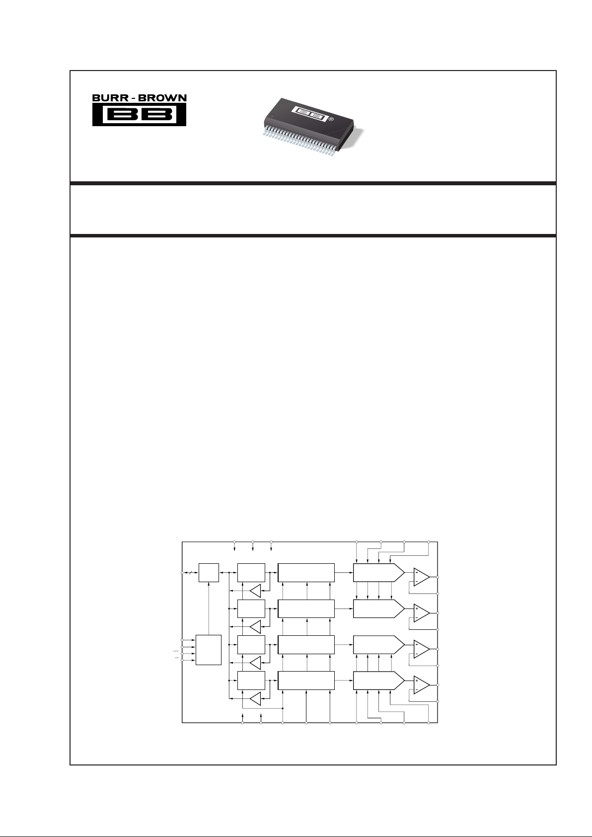
DAC7744
16-Bit, Quad Voltage Output
DIGITAL-TO-ANALOG CONVERTER
®
DAC7744
DESCRIPTION
The DAC7744 is a 16-bit, quad voltage output digitalto-analog converter with guaranteed 16-bit monotonic
performance over the specified temperature range. It
accepts 16-bit parallel input data, has double-buffered
DAC input logic (allowing simultaneous update of all
DACs), and provides a readback mode of the internal
input registers. Programmable asynchronous reset
clears all registers to a mid-scale code of 8000H or to
a zero-scale of 0000H. The DAC7744 operates from
either a single +15V supply or from a +15V, –15V,
and +5V supply.
Low power and small size per DAC make the DAC7744
ideal for automatic test equipment, DAC-per-pin programmers, data acquisition systems, and closed-loop
servo-control. The DAC7744 is available in a 48lead SSOP package, and offers guaranteed specifications over the –40°C to +85°C temperature range.
FEATURES
● LOW POWER: 200mW
● UNIPOLAR OR BIPOLAR OPERATION
● SINGLE-SUPPLY OUTPUT RANGE: +10V
● DUAL SUPPLY OUTPUT RANGE: ±10V
● SETTLING TIME: 10µs to 0.003%
● 16-BIT MONOTONICITY: –40°C to +85°C
● PROGRAMMABLE RESET TO MID-SCALE
OR ZERO-SCALE
● DATA READBACK
● DOUBLE-BUFFERED DATA INPUTS
APPLICATIONS
● PROCESS CONTROL
● ATE PIN ELECTRONICS
● CLOSED-LOOP SERVO-CONTROL
● MOTOR CONTROL
● DATA ACQUISITION SYSTEMS
● DAC-PER-PIN PROGRAMMERS
© 1999 Burr-Brown Corporation PDS-1534A Printed in U.S.A. November, 1999
DAC7744
International Airport Industrial Park • Mailing Address: PO Box 11400, Tucson, AZ 85734 • Street Address: 6730 S. Tucson Blvd., Tucson, AZ 85706 • Tel: (520) 746-1111
Twx: 910-952-1111 • Internet: http://www.burr-brown.com/ • Cable: BBRCORP • Telex: 066-6491 • FAX: (520) 889-1510 • Immediate Product Info: (800) 548-6132
For most current data sheet and other product
information, visit www.burr-brown.com
DAC A
DAC
Register A
Input
Register A
DAC7744
I/O
Buffer
Control
Logic
DAC B
DAC
Register B
Input
Register B
DAC C
DAC
Register C
Input
Register C
DAC D
DAC
Register D
Input
Register D
V
REF
L AB V
REF
H AB
V
REF
H
AB Sense
V
REF
L
AB Sense
V
OUT
D
V
OUT
C
V
OUT
B
V
OUT
A
V
OUTB
Sense
V
REF
L CD V
REF
H CD
RST LOADDACs
A1
A0
CS
R/W
DATA I/O
16
RSTSEL
AGND DGND
V
OUTC
Sense
V
OUTD
Sense
V
OUTA
Sense
V
CC
V
SS
V
DD
V
REF
L
CD Sense
V
REF
H
CD Sense
2
®
DAC7744
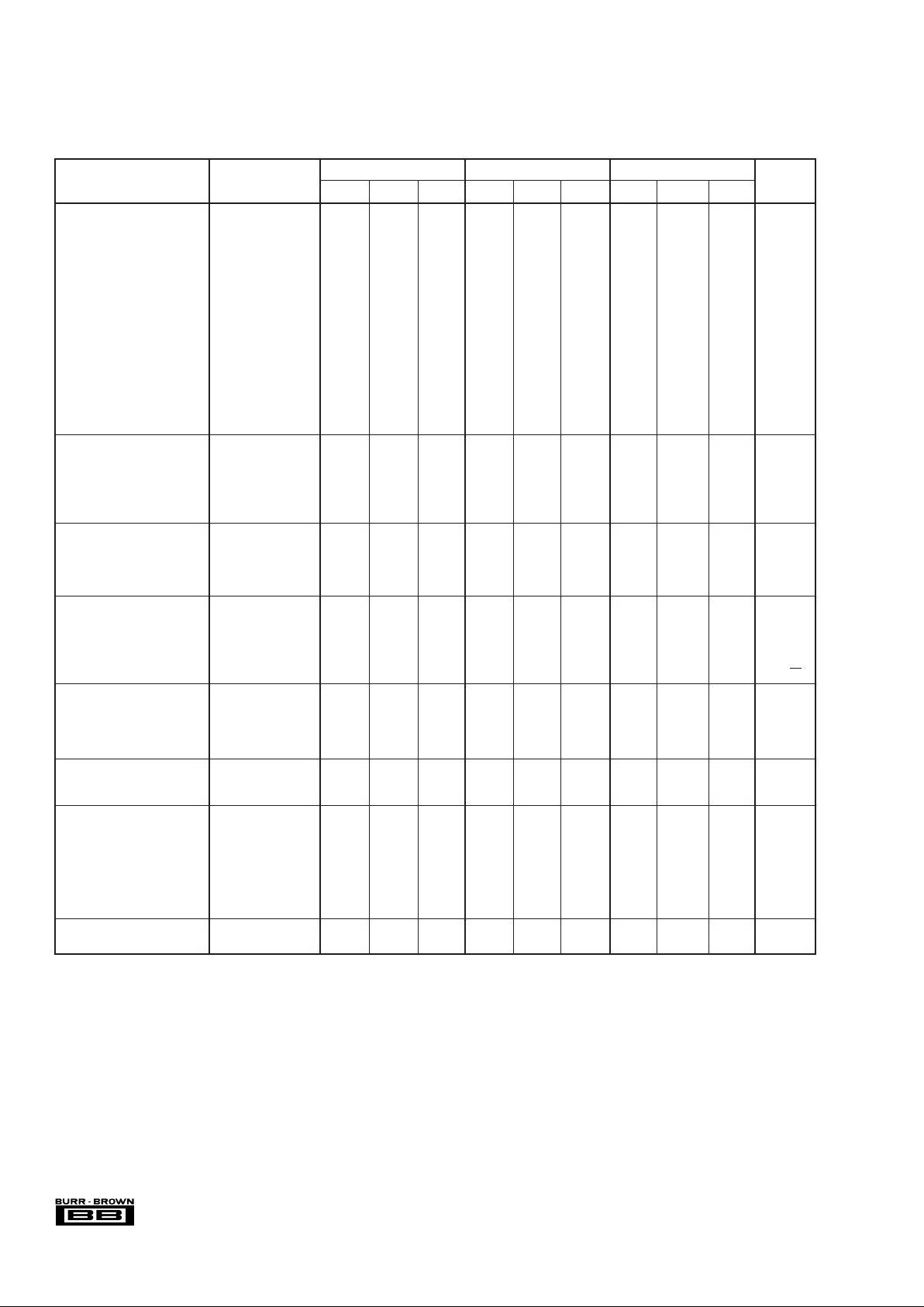
DAC7744E DAC7744EB DAC7744EC
PARAMETER CONDITIONS MIN TYP MAX MIN TYP MAX MIN TYP MAX UNITS
ACCURACY
Linearity Error T = 25°C ±3 ✻ ±2 LSB
T
MIN
to T
MAX
±4 ✻ ±3 LSB
Linearity Match ±4 ✻ ±2 LSB
Differential Linearity Error T = 25°C ±3 ±2 ±1 LSB
T
MIN
to T
MAX
±3 ±2 ±1 LSB
Monotonicity, T
MIN
to T
MAX
14 15 16 Bits
Bipolar Zero Error
T = 25°C ±0.01 ±0.025 ✻✻% of FSR
Bipolar Zero Error, T
MIN
to T
MAX
±0.05 ✻✻% of FSR
Full-Scale Error T = 25°C ±0.025 ✻✻% of FSR
Full-Scale Error, T
MIN
to T
MAX
±0.05 ✻✻% of FSR
Bipolar Zero Matching Channel-to-Channel ±0.024 ✻✻% of FSR
Matching
Full-Scale Matching Channel-to-Channel ±0.024 ✻✻% of FSR
Matching
Power Supply Rejection Ratio (PSRR)
At Full Scale 25 ✻✻ppm/V
ANALOG OUTPUT
Voltage Output V
REF
LV
REF
H ✻✻✻✻V
Output Current ±5 ✻✻ mA
Maximum Load Capacitance 500 ✻✻pF
Short-Circuit Current ±20 ✻✻mA
Short-Circuit Duration To V
SS
, V
DD
or GND Indefinite ✻✻
REFERENCE INPUT
Ref High Input Voltage Range
V
REF
L + 1.25
+10 ✻✻✻✻V
Ref Low Input Voltage Range –10
V
REF
H – 1.25
✻✻✻✻V
Ref High Input Current –0.3 2.6 ✻✻mA
Ref Low Input Current –3.2 –0.3 ✻✻mA
DYNAMIC PERFORMANCE
Settling Time To ±0.003%, 20V 9 11 ✻✻ ✻✻ µs
Output Step
Channel-to-Channel Crosstalk See Figure 5 0.5 ✻✻LSB
Digital Feedthrough 2 ✻✻nV-s
Output Noise Voltage f = 10kHz 60 ✻✻nV/√Hz
DIGITAL INPUT
V
IH
0.7 • V
DD
V
DD
✻✻ V
V
IL
0 0.3 • V
DD
✻ V
I
IH
±10 ✻ µA
I
IL
±10 ✻ µA
DIGITAL OUTPUT
V
OH
IOH = –0.8mA 3.6 4.5 ✻✻ ✻✻ V
V
OL
IOL = 1.6mA 0.3 0.4 ✻✻ ✻✻ V
POWER SUPPLY
V
DD
+4.75 +5.0 +5.25 ✻✻✻✻✻ ✻ V
V
CC
+14.25 +15.0 +15.75 ✻✻✻✻✻✻ V
V
SS
–14.25 –15.0 –15.75 ✻✻✻✻✻✻ V
I
DD
50 ✻✻µA
I
CC
6 ✻✻mA
I
SS
–5 ✻✻mA
Power 170 200 ✻✻mW
TEMPERATURE RANGE
Specified Performance –40 +85 ✻✻✻✻°C
✻ Specifications same as grade to the left.
The information provided herein is believed to be reliable; however, BURR-BROWN assumes no responsibility for inaccuracies or omissions. BURR-BROWN assumes
no responsibility for the use of this information, and all use of such information shall be entirely at the user’s own risk. Prices and specifications are subject to change
without notice. No patent rights or licenses to any of the circuits described herein are implied or granted to any third party. BURR-BROWN does not authorize or warrant
any BURR-BROWN product for use in life support devices and/or systems.
SPECIFICATIONS (Dual Supply)
At TA = T
MIN
to T
MAX
, VCC = +15V, VDD = +5V, VSS = –15V, V
REF
H = +10V, and V
REF
L = –10V, unless otherwise noted.
3
®
DAC7744
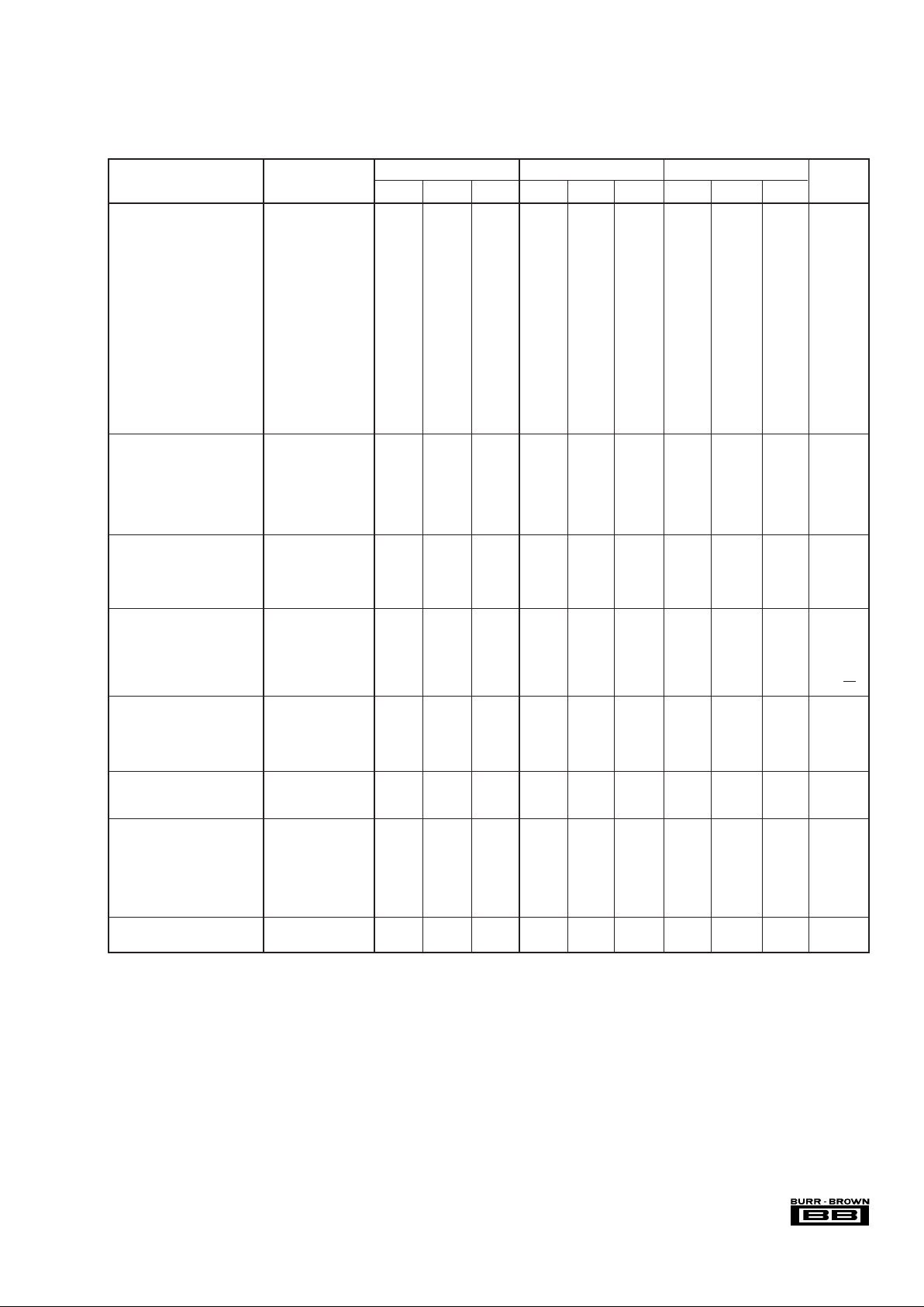
DAC7744E DAC7744EB DAC7744EC
PARAMETER CONDITIONS MIN TYP MAX MIN TYP MAX MIN TYP MAX UNITS
ACCURACY
Linearity Error
(1)
T = 25°C ±3 ✻ ±2 LSB
T
MIN
to T
MAX
±4 ✻ ±3 LSB
Linearity Match ±4 ✻ ±2 LSB
Differential Linearity Error T = 25°C ±3 ±2 ±1 LSB
T
MIN
to T
MAX
±3 ±2 ±1 LSB
Monotonicity, T
MIN
to T
MAX
14 15 16 Bits
Unipolar Zero T = 25°C ±0.01 ±0.025 ✻✻% of FSR
Unipolar Zero Error,
T
MIN
to T
MAX
±0.05 ✻✻% of FSR
Full-Scale Error T = 25°C ±0.025 ✻✻% of FSR
Full-Scale Error,
T
MIN
to T
MAX
±0.05 ✻✻% of FSR
Unipolar Zero Matching Channel-to-Channel ±0.024 ✻✻% of FSR
Matching
Full-Scale Matching Channel-to-Channel ±0.024 ✻✻% of FSR
Matching
Power Supply Rejection Ratio (PSRR)
At Full Scale 25 ✻✻ppm/V
ANALOG OUTPUT
Voltage Output V
REF
L = 0V, VSS = 0V 0 V
REF
H ✻✻✻✻V
R = 10kΩ
Output Current ±5 ✻✻ mA
Maximum Load Capacitance 500 ✻✻pF
Short-Circuit Current ±20 ✻✻mA
Short-Circuit Duration To V
SS
, V
CC
or GND Indefinite ✻✻
REFERENCE INPUT
Ref High Input Voltage Range
V
REF
L + 1.25
+10 ✻✻✻✻V
Ref Low Input Voltage Range 0
V
REF
H – 1.25
✻✻✻✻V
Ref High Input Current –0.3 1.0 ✻✻mA
Ref Low Input Current –1.5 –0.3 ✻✻mA
DYNAMIC PERFORMANCE
Settling Time To ±0.003%, 10V 8 10 ✻✻ ✻✻ µs
Output Step
Channel-to-Channel Crosstalk See Figure 6 0.5 ✻✻LSB
Digital Feedthrough 2 ✻✻nV-s
Output Noise Voltage f = 10kHz 60 ✻✻nV/√Hz
DIGITAL INPUT
V
IH
0.7 • V
DD
V
DD
✻✻ V
V
IL
0 0.3 • V
DD
✻ V
I
IH
±10 ✻ µA
I
IL
±10 ✻ µA
DIGITAL OUTPUT
V
OH
IOH = –0.8mA 3.6 4.5 ✻✻ ✻✻ V
V
OL
IOL = 1.6mA 0.3 0.4 ✻✻ ✻✻ V
POWER SUPPLY
V
DD
+4.75 +5.0 +5.25 ✻✻✻✻✻✻ V
V
CC
+14.25 +15.0 +15.75 ✻✻✻✻✻✻ V
V
SS
0 ✻✻V
I
DD
50 ✻✻µA
I
CC
3.5 ✻✻mA
Power 50 70 ✻✻mW
TEMPERATURE RANGE
Specified Performance –40 +85 ✻✻✻✻°C
✻ Specifications same as grade to the left.
NOTE: (1) If V
SS
= 0V, the specification applies at code 0021H and above, due to possible negative zero scale error.
SPECIFICATIONS (Single Supply)
At TA = T
MIN
to T
MAX
, VCC = +15V, VDD = +5V, VSS = GND, V
REF
H = +10V, and V
REF
L = +50mV, unless otherwise noted.
4
®
DAC7744
ABSOLUTE MAXIMUM RATINGS
(1)
V
CC
to VSS...........................................................................–0.3V to +32V
V
CC
to AGND ...................................................................... –0.3V to +16V
V
SS
to AGND ...................................................................... +0.3V to –16V
AGND
to DGND................................................................. –0.3V to +0.3V
V
REFH
to AGND ..................................................................... –9V to +11V
V
REFL
to AGND...................................................................... –11V to +9V
V
DD
to GND ........................................................................... –0.3V to +6V
V
REFH
to V
REF
L ........................................................................ –1V to 22V
Digital Input Voltage to GND ................................... –0.3V to V
DD
+ 0.3V
Digital Output Voltage to GND................................. –0.3V to V
DD
+ 0.3V
Maximum Junction Temperature................................................... +150 °C
Operating Temperature Range ........................................–40°C to +85°C
Storage Temperature Range .........................................–65°C to +150°C
Lead Temperature (soldering, 10s)............................................... +300°C
NOTE: (1) Stresses above those listed under “Absolute Maximum Ratings”
may cause permanent damage to the device. Exposure to absolute maximum
conditions for extended periods may affect device reliability.
ELECTROSTATIC
DISCHARGE SENSITIVITY
This integrated circuit can be damaged by ESD. Burr-Brown
recommends that all integrated circuits be handled with
appropriate precautions. Failure to observe proper handling
and installation procedures can cause damage.
ESD damage can range from subtle performance degradation
to complete device failure. Precision integrated circuits may
be more susceptible to damage because very small parametric
changes could cause the device not to meet its published
specifications.
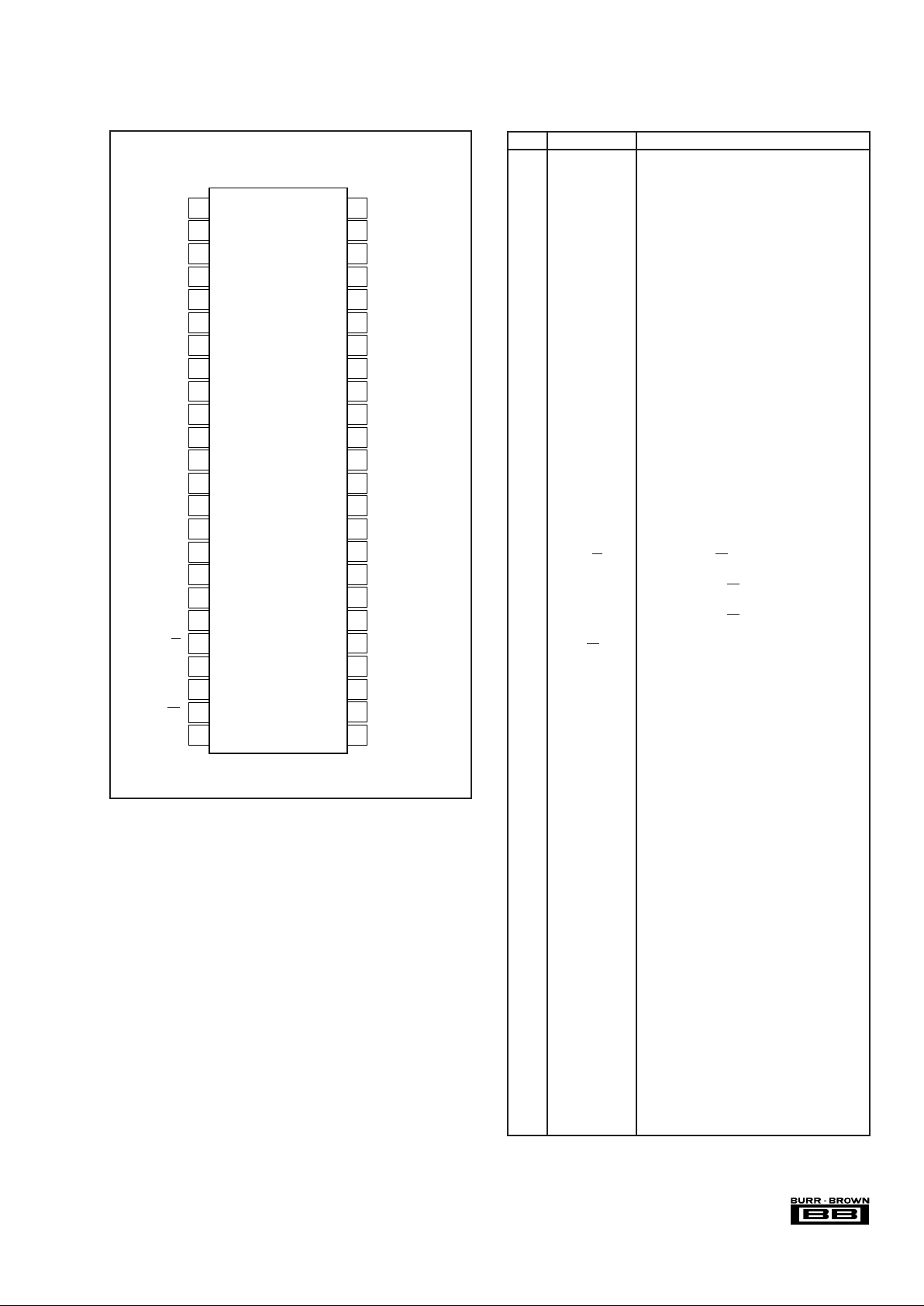
PACKAGE/ORDERING INFORMATION
LINEARITY DIFFERENTIAL PACKAGE SPECIFICATION
ERROR NONLINEARITY DRAWING TEMPERATURE ORDERING TRANSPORT
PRODUCT (LSB) (LSB) PACKAGE NUMBER RANGE NUMBER
(1)
MEDIA
DAC7744E ±4 ±3 48-Lead SSOP 333 –40°C to +85°C DAC7744E Rails
"" """ "DAC7744E/1K Tape and Reel
DAC7744EB ±4 ±2 48-Lead SSOP 333 –40°C to +85°C DAC7744EB Rails
"" """ "DAC7744EB/1K Tape and Reel
DAC7744EC ±3 ±1 48-Lead SSOP 333 –40°C to +85°C DAC7744EC Rails
"" """ "DAC7744EC/1K Tape and Reel
NOTE: (1) Models with a slash (/) are available only in Tape and Reel in the quantities indicated (e.g., /1K indicates 1000 devices per reel). Ordering 1000 pieces
of “DAC7744E/1K” will get a single 1000-piece Tape and Reel.
RefH
V
OUT
Sense
V
CC
V
SS
V
DD
DGND
4
V
CC
AGND
V
SS
V
DD
DGND
V
OUT
RefH Sense
RefL Sense
RefL
1 of 2
1 of 4
Typ of Each
Logic Input Pin
Typ of Each
I/O Pin
ESD PROTECTION CIRCUITS
5
®
DAC7744
PIN DESCRIPTIONS
PIN NAME DESCRIPTION
1 DB15 Data Bit 15, MSB
2 DB14 Data Bit 14
3 DB13 Data Bit 13
4 DB12 Data Bit 12
5 DB11 Data Bit 11
6 DB10 Data Bit 10
7 DB9 Data Bit 9
8 DB8 Data Bit 8
9 DB7 Data Bit 7
10 DB6 Data Bit 6
11 DB5 Data Bit 5
12 DB4 Data Bit 4
13 DB3 Data Bit 3
14 DB2 Data Bit 2
15 DB1 Data Bit 1
16 DB0 Data Bit 0, LSB
17 RSTSEL Reset Select. Determines the action of RST. If
HIGH, a RST command will set the DAC registers to mid-scale. If LOW, a RST command will
set the DAC registers to zero.
18 RST Reset, Edge-Triggered. Depending on the state
of RSTSEL, the DAC Input and Output registers
are set to either mid-scale or zero.
19 LOADDACs DAC Output Registers Load Control. Rising edge
triggered.
20 R/W Enabled by the CS, controls data read and write
from the input register.
21 A1 Enabled by the CS, in combination with A0
selects the Individual DAC Input Registers.
22 A0 Enabled by the CS, in combination with A1
selects the individual DAC input registers.
23 CS Chip Select, Active LOW.
24 DGND Digital Ground
25 V
DD
Positive Power Supply
26 V
CC
Positive Power Supply
27 AGND Analog Ground
28 V
SS
Negative Power Supply
29 V
OUT
D DAC D Voltage Output
30 V
OUT
D Sense DAC D’s Output Amplifier Inverting Input. Used
to close the feedback loop at the load.
31 V
REF
L CD Sense DAC C and D Reference Low Sense Input
32 V
REF
L CD DAC C and D Reference Low Input
33 V
REF
H CD DAC C and D Reference High Input
34 V
REF
H CD Sense DAC C and D Reference High Sense Input
35 V
OUT
C DAC C Voltage Output
36 V
OUT
C Sense DAC C’s Output Amplifier Inverting Input. Used
to close the feedback loop at the load.
37 V
OUT
B DAC B Voltage Output
38 V
OUT
B Sense DAC B’s Output Amplifier Inverting Input. Used
to close the feedback loop at the load.
39 V
REF
H AB Sense DAC A and B Reference High Sense Input
40 V
REF
H AB DAC A and B Reference High Input
41 V
REF
L AB DAC A and B Reference Low Input
42 V
REF
L AB Sense DAC A and B Reference Low Sense Input
43 V
OUT
A DAC A Voltage Input
44 V
OUT
A Sense DAC A’s Output Amplifier Inverting Input. Used
to close the feedback loop at the load.
45 NC No Connection
46 NC No Connection
47 NC No Connection
48 NC No Connection
Top View SSOP
PIN CONFIGURATION
DB15 (MSB)
DB14
DB13
DB12
DB11
DB10
DB9
DB8
DB7
DB6
DB5
DB4
DB3
DB2
DB1
DB0 (LSB)
RSTSEL
RST
LOADDACs
R/W
A1
A0
CS
DGND
NC
NC
NC
NC
V
OUT
A Sense
V
OUT
A
V
REF
L AB Sense
V
REF
L AB
V
REF
H AB
V
REF
H AB Sense
V
OUT
B Sense
V
OUT
B
V
OUT
C Sense
V
OUT
C
V
REF
H CD Sense
V
REF
H CD
V
REF
L CD
V
REF
L CD Sense
V
OUT
D Sense
V
OUT
D
V
SS
AGND
V
CC
V
DD
1
2
3
4
5
6
7
8
9
10
11
12
13
14
15
16
17
18
19
20
21
22
23
24
48
47
46
45
44
43
42
41
40
39
38
37
36
35
34
33
32
31
30
29
28
27
26
25
DAC7744
6
®
DAC7744
TYPICAL PERFORMANCE CURVES: VSS = 0V
At TA = +25°C, VDD = +5V, VCC = +15V, V
SS
= 0, V
REFH
= +10V, and V
REFL
= 0V, representative unit, unless otherwise specified.
2.0
1.5
1.0
0.5
0
–0.5
–1.0
–1.5
–2.0
2.0
1.5
1.0
0.5
0
–0.5
–1.0
–1.5
–2.0
LE (LSB)DLE (LSB)
LINEARITY ERROR AND
DIFFERENTIAL LINEARITY ERROR vs CODE
(DAC A, +25°C)
0000H2000H4000H6000H8000
H
Digital Input Code
A000
H
C000HE000HFFFF
H
2.0
1.5
1.0
0.5
0
–0.5
–1.0
–1.5
–2.0
2.0
1.5
1.0
0.5
0
–0.5
–1.0
–1.5
–2.0
LE (LSB)DLE (LSB)
LINEARITY ERROR AND
DIFFERENTIAL LINEARITY ERROR vs CODE
(DAC B, +25°C)
0000H2000H4000H6000H8000
H
Digital Input Code
A000
H
C000HE000HFFFF
H
2.0
1.5
1.0
0.5
0
–0.5
–1.0
–1.5
–2.0
2.0
1.5
1.0
0.5
0
–0.5
–1.0
–1.5
–2.0
LE (LSB)DLE (LSB)
LINEARITY ERROR AND
DIFFERENTIAL LINEARITY ERROR vs CODE
(DAC C, +25°C)
0000H2000H4000H6000H8000
H
Digital Input Code
A000
H
C000HE000HFFFF
H
2.0
1.5
1.0
0.5
0
–0.5
–1.0
–1.5
–2.0
2.0
1.5
1.0
0.5
0
–0.5
–1.0
–1.5
–2.0
LE (LSB)DLE (LSB)
LINEARITY ERROR AND
DIFFERENTIAL LINEARITY ERROR vs CODE
(DAC D, +25°C)
0000H2000H4000H6000H8000
H
Digital Input Code
A000
H
C000HE000HFFFF
H
2.0
1.5
1.0
0.5
0
–0.5
–1.0
–1.5
–2.0
2.0
1.5
1.0
0.5
0
–0.5
–1.0
–1.5
–2.0
LE (LSB)DLE (LSB)
LINEARITY ERROR AND
DIFFERENTIAL LINEARITY ERROR vs CODE
(DAC B, +85°C)
0000H2000H4000H6000H8000
H
Digital Input Code
A000
H
C000HE000HFFFF
H
+25°C
+85°C
2.0
1.5
1.0
0.5
0
–0.5
–1.0
–1.5
–2.0
2.0
1.5
1.0
0.5
0
–0.5
–1.0
–1.5
–2.0
LE (LSB)DLE (LSB)
LINEARITY ERROR AND
DIFFERENTIAL LINEARITY ERROR vs CODE
(DAC A, +85°C)
0000H2000H4000H6000H8000
H
Digital Input Code
A000
H
C000HE000HFFFF
H
7
®
DAC7744
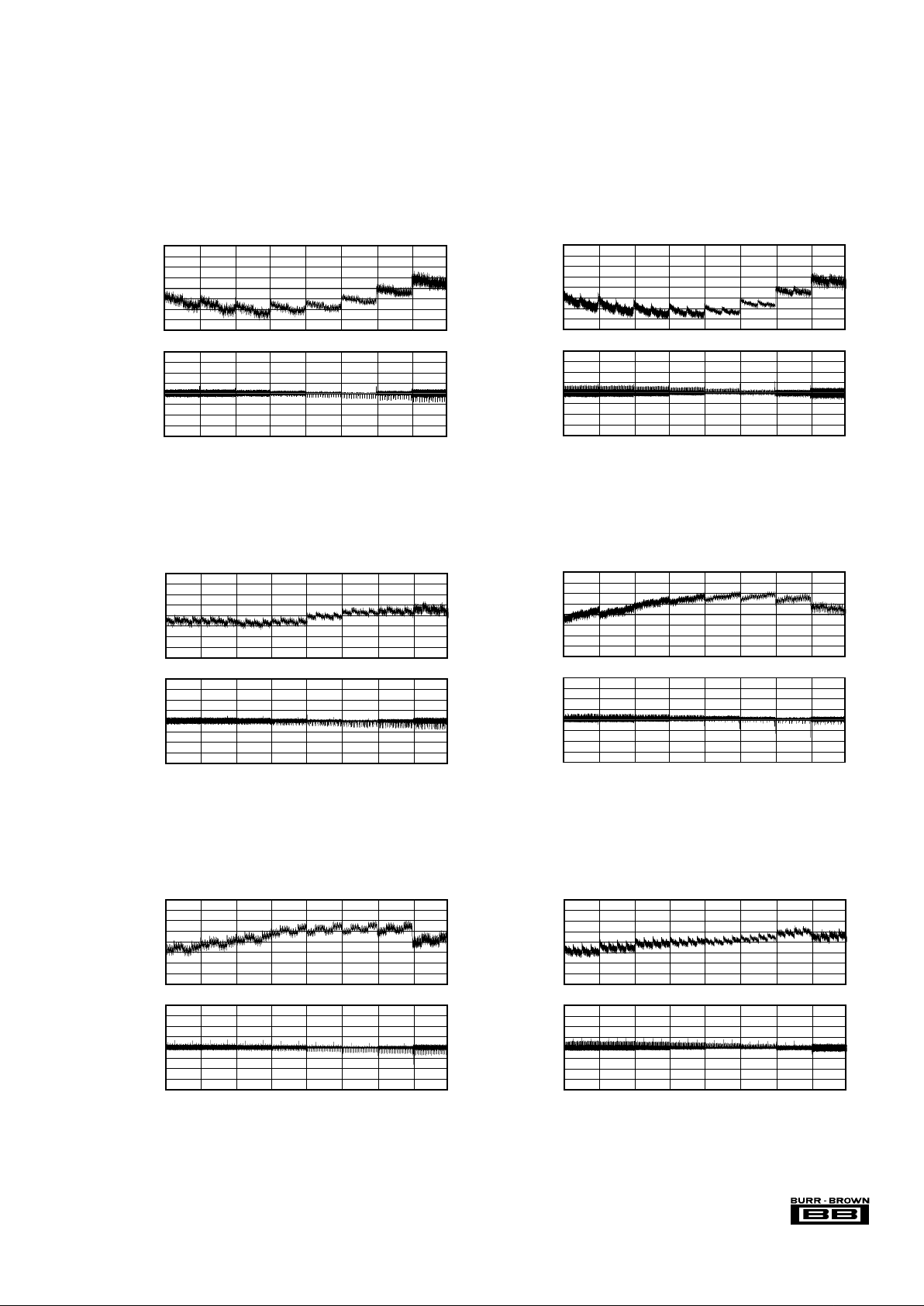
TYPICAL PERFORMANCE CURVES: VSS = 0V (Cont.)
At TA = +25°C, VDD = +5V, VCC = +15V, V
SS
= 0, V
REFH
= +10V, and V
REFL
= 0V, representative unit, unless otherwise specified.
2.0
1.5
1.0
0.5
0
–0.5
–1.0
–1.5
–2.0
2.0
1.5
1.0
0.5
0
–0.5
–1.0
–1.5
–2.0
LE (LSB)DLE (LSB)
LINEARITY ERROR AND
DIFFERENTIAL LINEARITY ERROR vs CODE
(DAC C, +85°C)
0000H2000H4000H6000H8000
H
Digital Input Code
A000
H
C000HE000HFFFF
H
2.0
1.5
1.0
0.5
0
–0.5
–1.0
–1.5
–2.0
2.0
1.5
1.0
0.5
0
–0.5
–1.0
–1.5
–2.0
LE (LSB)DLE (LSB)
LINEARITY ERROR AND
DIFFERENTIAL LINEARITY ERROR vs CODE
(DAC D, +85°C)
0000H2000H4000H6000H8000
H
Digital Input Code
A000
H
C000HE000HFFFF
H
2.0
1.5
1.0
0.5
0
–0.5
–1.0
–1.5
–2.0
2.0
1.5
1.0
0.5
0
–0.5
–1.0
–1.5
–2.0
LE (LSB)DLE (LSB)
LINEARITY ERROR AND
DIFFERENTIAL LINEARITY ERROR vs CODE
(DAC A, –40°C)
0000H2000H4000H6000H8000
H
Digital Input Code
A000
H
C000HE000HFFFF
H
2.0
1.5
1.0
0.5
0
–0.5
–1.0
–1.5
–2.0
2.0
1.5
1.0
0.5
0
–0.5
–1.0
–1.5
–2.0
LE (LSB)DLE (LSB)
LINEARITY ERROR AND
DIFFERENTIAL LINEARITY ERROR vs CODE
(DAC B, –40°C)
0000H2000H4000H6000H8000
H
Digital Input Code
A000
H
C000HE000HFFFF
H
2.0
1.5
1.0
0.5
0
–0.5
–1.0
–1.5
–2.0
2.0
1.5
1.0
0.5
0
–0.5
–1.0
–1.5
–2.0
LE (LSB)DLE (LSB)
LINEARITY ERROR AND
DIFFERENTIAL LINEARITY ERROR vs CODE
(DAC C, –40°C)
0000H2000H4000H6000H8000
H
Digital Input Code
A000HC000HE000HFFFF
H
2.0
1.5
1.0
0.5
0
–0.5
–1.0
–1.5
–2.0
2.0
1.5
1.0
0.5
0
–0.5
–1.0
–1.5
–2.0
LE (LSB)DLE (LSB)
LINEARITY ERROR AND
DIFFERENTIAL LINEARITY ERROR vs CODE
(DAC D, –40°C)
0000H2000H4000H6000H8000
H
Digital Input Code
A000
H
C000HE000HFFFF
H
+85°C (cont.)
–40°C
 Loading...