

Burr Brown Corporation DAC7625UB-1K, DAC7625UB, DAC7625U-1K, DAC7625U, DAC7625PB Datasheet
...
1
®
DAC7624/7625
12-Bit Quad Voltage Output
DIGITAL-TO-ANALOG CONVERTER
International Airport Industrial Park • Mailing Address: PO Box 11400, Tucson, AZ 85734 • Street Address: 6730 S. Tucson Blvd., Tucson, AZ 85706 • Tel: (520) 746-1111 • Twx: 910-952-1111
Internet: http://www.burr-brown.com/ • FAXLine: (800) 548-6133 (US/Canada Only) • Cable: BBRCORP • Telex: 066-6491 • FAX: (520) 889-1510 • Immediate Product Info: (800) 548-6132
®
DAC7624
DAC7625
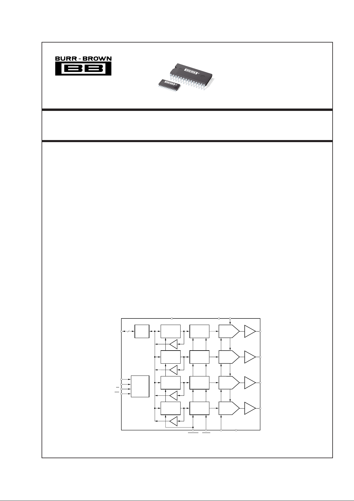
DESCRIPTION
The DAC7624 and DAC7625 are 12-bit quad voltage
output digital-to-analog converters with guaranteed 12bit monotonic performance over the specified temperature range. They accept 12-bit parallel input data, have
double-buffered DAC input logic (allowing simultaneous update of all DACs), and provide a readback
mode of the internal input registers. An asynchronous
reset clears all registers to a mid-scale code of 800
H
(DAC7624) or to a zero-scale of 000H (DAC7625). The
DAC7624 and DAC7625 can operate from a single +5V
supply or from +5V and –5V supplies.
Low power and small size per DAC make the DAC7624
and DAC7625 ideal for automatic test equipment,
DAC-per-pin programmers, data acquisition systems,
and closed-loop servo-control. The DAC7624 and
DAC7625 are available in a 28-pin plastic doublewide or a 28-lead SOIC package, and offer guaranteed
specifications over the –40°C to +85°C temperature
range.
FEATURES
● LOW POWER: 20mW
● UNIPOLAR OR BIPOLAR OPERATION
● SETTLING TIME: 10µs to 0.012%
● 12-BIT LINEARITY AND MONOTONICITY:
–40°C to +85°C
● RESET TO MID-SCALE (DAC7624) OR
ZERO-SCALE (DAC7625)
● DATA READBACK
● DOUBLE-BUFFERED DATA INPUTS
APPLICATIONS
● PROCESS CONTROL
● ATE PIN ELECTRONICS
● CLOSED-LOOP SERVO-CONTROL
● MOTOR CONTROL
● DATA ACQUISITION SYSTEMS
● DAC-PER-PIN PROGRAMMERS
DAC7624
DAC7625
© 1997 Burr-Brown Corporation PDS-1419C Printed in U.S.A. April, 2000
DAC A
DAC
Register A
Input
Register A
I/O
Buffer
Control
Logic
DAC B
DAC
Register B
Input
Register B
DAC C
DAC
Register C
Input
Register C
DAC D
DAC
Register D
Input
Register D
V
REFH
V
DD
V
SS
V
OUTD
V
OUTC
V
OUTB
V
OUTA
V
REFLRESET LDAC
GND
A0
A1
R/W
CS
DB0-DB11
12
2
®
DAC7624/7625
SPECIFICATION
At TA = –40°C to +85°C, VDD = +5V, VSS = –5V, V
REFH
= +2.5V, V
REFL
= –2.5V, unless otherwise noted.
The information provided herein is believed to be reliable; however, BURR-BROWN assumes no responsibility for inaccuracies or omissions. BURR-BROWN assumes
no responsibility for the use of this information, and all use of such information shall be entirely at the user’s own risk. Prices and specifications are subject to change
without notice. No patent rights or licenses to any of the circuits described herein are implied or granted to any third party. BURR-BROWN does not authorize or warrant
any BURR-BROWN product for use in life support devices and/or systems.
DAC7624P, U DAC7624PB, UB
DAC7625P, U DAC7625PB, UB
NOTES: (1) If VSS = 0V, specification applies at code 00AH and above. (2) LSB means Least Significant Bit, when V
REFH
equals +2.5V and V
REFL
equals –2.5V,
then one LSB equals 1.22mV. (3) All DAC outputs will match within the specified error band. (4) Ideal output voltage, does not take into account zero or full-scale
error. (5) If V
SS
= –5V, full-scale 5V step. If VSS = 0V, full-scale positive 2.5V step and negative step from code FFFH to 00AH.
PARAMETER CONDITIONS MIN TYP MAX MIN TYP MAX UNITS
ACCURACY
Linearity Error
(1)
VSS = 0V or –5V ±2 ±1 LSB
(2)
Linearity Matching
(3)
VSS = 0V or –5V ±2 ±1 LSB
Differential Linearity Error VSS = 0V or –5V ±1 ±1 LSB
Monotonicity T
MIN
to T
MAX
12 ✻ Bits
Zero-Scale Error Code = 000
H
±4 ✻ LSB
Zero-Scale Drift 25 ✻✻ppm/°C
Zero-Scale Matching
(3)
±2 ±1 LSB
Full-Scale Error Code = FFF
H
±4 ✻ LS
Full-Scale Matching
(3)
±2 ±1 LSB
Zero-Scale Error Code = 00A
H
, VSS = 0V ±8 ✻ LSB
Zero-Scale Drift VSS = 0V 5 10 ✻✻ppm/°C
Zero-Scale Matching
(3)
VSS = 0V ±4 ±2 LSB
Full-Scale Error Code = FFF
H
, VSS = 0V ±8 ✻ LSB
Full-Scale Matching
(3)
VSS = 0V ±4 ±2 LSB
Power Supply Rejection 30 ✻ ppm/V
ANALOG OUTPUT
Voltage Output
(4)
V
REFL
= 0V, VSS = 0V 0 V
REFH
✻✻V
V
SS
= –5V V
REFL
V
REFH
✻✻V
Output Current –1.25 +1.25 ✻✻mA
Load Capacitance No Oscillation 100 ✻ pF
Short-Circuit Current +5, –120 ✻ mA
Short-Circuit Duration
Momentary
✻
REFERENCE INPUT
V
REFH
Input Range VSS = 0V or –5V
V
REFL
+1.25
+2.5 ✻✻V
V
REFL
Input Range VSS = 0V 0
V
REFH
–1.25
✻✻V
V
REFL
Input Range VSS = –5V –2.5
V
REFH
–1.25
✻✻V
DYNAMIC PERFORMANCE
Settling Time
(5)
To ±0.012% 5 10 ✻✻ µs
Channel-to-Channel Crosstalk
Full-Scale Step
0.25 ✻ LSB
On any other DAC
Output Noise Voltage 0Hz to 1MHz 40 ✻ nV/√Hz
DIGITAL INPUT/OUTPUT
Logic Family TTL-Compatible CMOS ✻
Logic Levels
V
IH
IIH ≤ ±10µA 2.4 VDD +0.3 ✻✻V
V
IL
IIL ≤ ±10µA –0.3 0.8 ✻✻V
V
OH
IOH = –0.8mA 3.6 V
DD
✻✻V
V
OL
IOL = 1.6mA 0.0 0.4 ✻✻V
Data Format Straight Binary ✻
POWER SUPPLY REQUIREMENTS
V
DD
4.75 5.25 ✻✻V
V
SS
If VSS ≠ 0V –5.25 –4.75 ✻✻V
I
DD
1.5 1.9 ✻✻ mA
I
SS
–2.1 –1.6 ✻✻ mA
Power Dissipation VSS = –5V 15 20 ✻✻ mW
V
SS
= 0V 7.5 10 ✻✻ mW
TEMPERATURE RANGE
Specified Performance DAC7624P, U, PB, UB –40 +85 ✻✻°C
DAC7625P, U, PB, UB

3
®
DAC7624/7625
ABSOLUTE MAXIMUM RATINGS
(1)
V
DD
to VSS............................................................................. –0.3V to 11V
V
DD
to GND .......................................................................... –0.3V to 5.5V
V
REFL
to VSS..............................................................–0.3V to (V
DD
– VSS)
V
DD
to V
REFH
............................................................. –0.3V to (V
DD
– VSS)
V
REFH
to V
REFL
..........................................................–0.3V to (V
DD
– VSS)
Digital Input Voltage to GND ................................... –0.3V to V
DD
+ 0.3V
Digital Output Voltage to GND ................................. –0.3V to V
DD
+ 0.3V
Maximum Junction Temperature................................................... +150°C
Operating Temperature Range ........................................ –40°C to +85°C
Storage Temperature Range .........................................–65°C to +150°C
Lead Temperature (soldering, 10s) ............................................... +300°C
NOTE: (1) Stresses above those listed under “Absolute Maximum Ratings”
may cause permanent damage to the device. Exposure to absolute maximum
conditions for extended periods may affect device reliability.
ELECTROSTATIC
DISCHARGE SENSITIVITY
This integrated circuit can be damaged by ESD. Burr-Brown
recommends that all integrated circuits be handled with
appropriate precautions. Failure to observe proper handling
and installation procedures can cause damage.
ESD damage can range from subtle performance degradation
to complete device failure. Precision integrated circuits may
be more susceptible to damage because very small parametric
changes could cause the device not to meet its published
specifications.
PACKAGE/ORDERING INFORMATION
MAXIMUM
MAXIMUM DIFFERENTIAL SPECIFICATION PACKAGE
LINEARITY LINEARITY TEMPERATURE DRAWING
PRODUCT ERROR (LSB) ERROR (LSB) RANGE PACKAGE NUMBER
(1)
DAC7624P ±2 ±1 –40°C to +85°C 28-Pin Plastic DIP 215
DAC7624U ±2 ±1 –40°C to +85°C 28-Lead SOIC 217
DAC7624PB ±1 ±1 –40°C to +85°C 28-Pin Plastic DIP 215
DAC7624UB ±1 ±1 –40°C to +85°C 28-Lead SOIC 217
DAC7625P ±2 ±1 –40°C to +85°C 28-Pin Plastic DIP 215
DAC7625U ±2 ±1 –40°C to +85°C 28-Lead SOIC 217
DAC7625PB ±1 ±1 –40°C to +85°C 28-Pin Plastic DIP 215
DAC7625UB ±1 ±1 –40°C to +85°C 28-Lead SOIC 217
NOTE: (1) For detailed drawing and dimension table, please see end of data sheet, or Appendix C of Burr-Brown IC Data Book.
4
®
DAC7624/7625
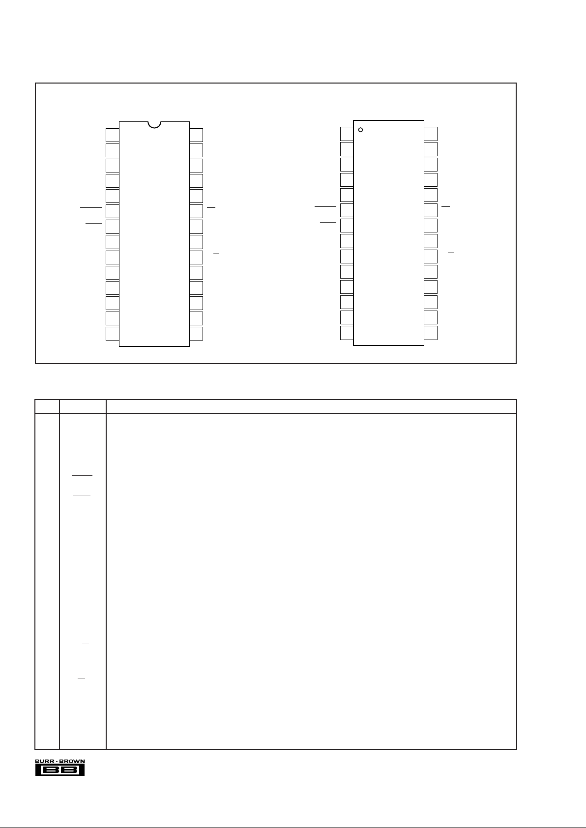
1
2
3
4
5
6
7
8
9
10
11
12
13
14
V
REFH
V
OUTB
V
OUTA
V
SS
GND
RESET
LDAC
(LSB) DB0
DB1
DB2
DB3
DB4
DB5
DB6
V
REFL
V
OUTC
V
OUTD
V
DD
NIC
CS
A0
A1
R/W
DB11 (MSB)
DB10
DB9
DB8
DB7
28
27
26
25
24
23
22
21
20
19
18
17
16
15
DAC7624
DAC7625
1
2
3
4
5
6
7
8
9
10
11
12
13
14
V
REFH
V
OUTB
V
OUTA
V
SS
GND
RESET
LDAC
(LSB) DB0
DB1
DB2
DB3
DB4
DB5
DB6
V
REFL
V
OUTC
V
OUTD
V
DD
NIC
CS
A0
A1
R/W
DB11 (MSB)
DB10
DB9
DB8
DB7
28
27
26
25
24
23
22
21
20
19
18
17
16
15
DAC7624
DAC7625
Top View
DIP SOIC
PIN DESCRIPTIONS
PIN CONFIGURATIONS
PIN NAME DESCRIPTION
1V
REFH
Reference Input Voltage High. Sets maximum output voltage for all DACs.
2V
OUTB
DAC B Voltage Output.
3V
OUTA
DAC A Voltage Output.
4V
SS
Negative Analog Supply Voltage, 0V or –5V.
5 GND Ground.
6 RESET Asynchronous Reset Input. Sets DAC and input registers to either mid-scale (800
H
, DAC7624) or zero-scale (000H, DAC7625)
when LOW.
7 LDAC Load DAC Input. All DAC Registers are transparent when LOW.
8 DB0 Data Bit 0. Least significant bit of 12-bit word.
9 DB1 Data Bit 1
10 DB2 Data Bit 2
11 DB3 Data Bit 3
12 DB4 Data Bit 4
13 DB5 Data Bit 5
14 DB6 Data Bit 6
15 DB7 Data Bit 7
16 DB8 Data Bit 8
17 DB9 Data Bit 9
18 DB10 Data Bit 10
19 DB11 Data Bit 11. Most significant bit of 12-bit word.
20 R/W Read/Write Control Input (read = HIGH, write = LOW).
21 A1 Register/DAC Select (C or D = HIGH, A or B = LOW).
22 A0 Register/DAC Select (B or D = HIGH, A or C = LOW).
23 CS Chip Select Input.
24 NIC Not Internally Connected. Pin has no internal connection to the device.
25 V
DD
Positive Analog Supply Voltage, +5V nominal.
26 V
OUTD
DAC D Voltage Output.
27 V
OUTC
DAC C Voltage Output.
28 V
REFL
Reference Input Voltage Low. Sets minimum output voltage for all DACs.
 Loading...