


Burr Brown Corporation DAC7614UB-1K, DAC7614UB, DAC7614U-1K, DAC7614U, DAC7614PB Datasheet
...
DAC7614
DAC7614
DAC7614
®
© 1998 Burr-Brown Corporation PDS-1445C Printed in U.S.A. December, 1998
Quad, Serial Input, 12-Bit, Voltage Output
DIGITAL-TO-ANALOG CONVERTER
FEATURES
● LOW POWER: 20mW
● UNIPOLAR OR BIPOLAR OPERATION
● SETTLING TIME: 10µs to 0.012%
● 12-BIT LINEARITY AND MONOTONICITY:
–40°C to +85°C
● USER SELECTABLE RESET TO MID-
SCALE OR ZERO-SCALE
● SECOND-SOURCE for DAC8420
● SMALL 20-LEAD SSOP PACKAGE
APPLICATIONS
● ATE PIN ELECTRONICS
● PROCESS CONTROL
● CLOSED-LOOP SERVO-CONTROL
● MOTOR CONTROL
● DATA ACQUISITION SYSTEMS
DESCRIPTION
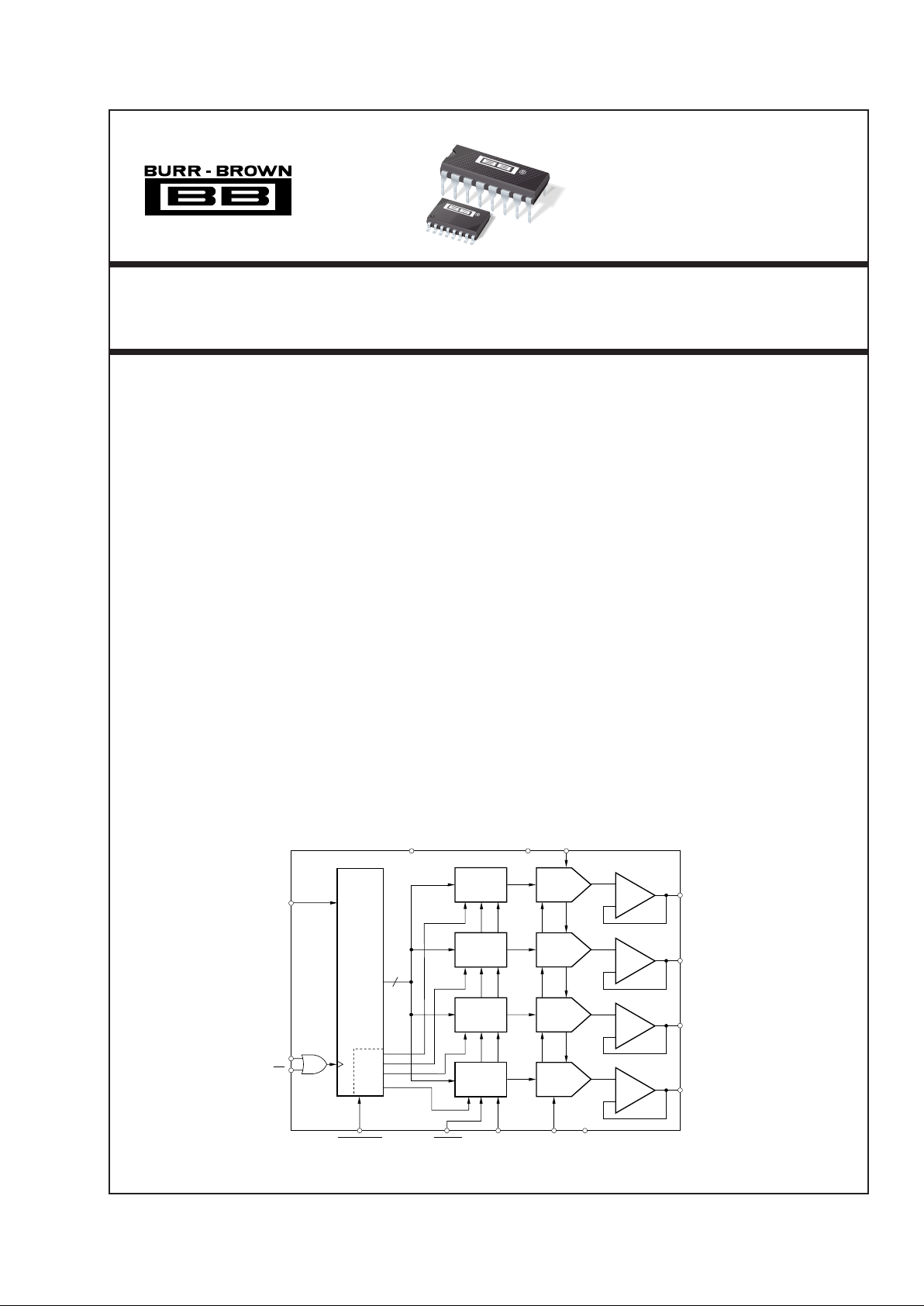
The DAC7614 is a quad, serial input, 12-bit, voltage
output digital-to-analog converter (DAC) with guaranteed 12-bit monotonic performance over the –40°C
to +85°C temperature range. An asynchronous reset
clears all registers to either mid-scale (800H) or zeroscale (000H), selectable via the RESETSEL pin. The
device can be powered from a single +5V supply or
from dual +5V and –5V supplies.
International Airport Industrial Park • Mailing Address: PO Box 11400, Tucson, AZ 85734 • Street Address: 6730 S. Tucson Blvd., Tucson, AZ 85706 • Tel: (520) 746-1111
Twx: 910-952-1111 • Internet: http://www.burr-brown.com/ • Cable: BBRCORP • Telex: 066-6491 • FAX: (520) 889-1510 • Immediate Product Info: (800) 548-6132
Low power and small size makes the DAC7614 ideal
for process control, data acquisition systems, and
closed-loop servo-control. The device is available in
16-pin plastic DIP, 16-lead SOIC, or 20-lead SSOP
packages, and is guaranteed over the –40°C to +85°C
temperature range.
DAC A
DAC
Register A
DAC B
DAC
Register B
DAC C
DAC
Register C
DAC D
DAC
Register D
V
REFH
V
DD
V
SS
V
OUTD
V
OUTC
V
OUTB
V
OUTA
V
REFL
GND
CLK
CS
12
SDI
RESET RESETSELLOADDACS
Serial-to-
Parallel
Shift
Register
DAC
Select
®
2
DAC7614
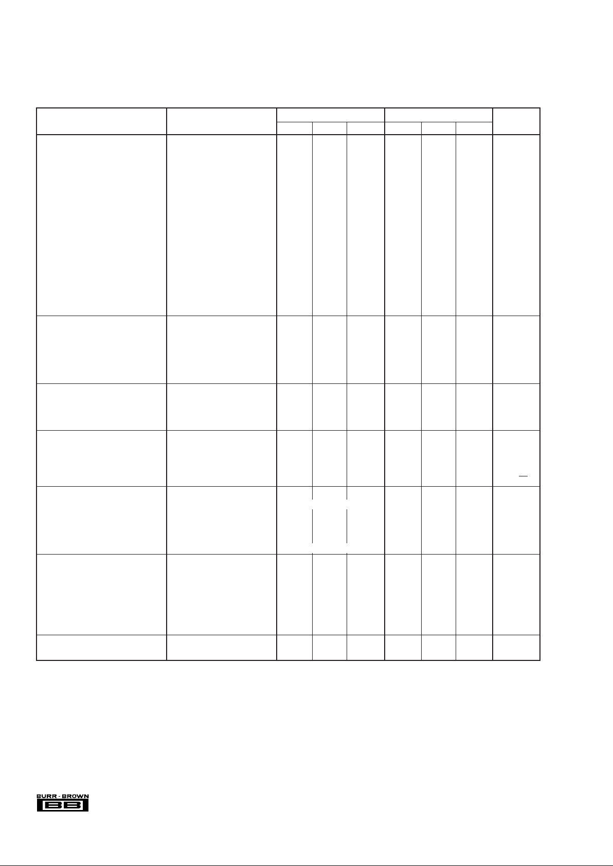
SPECIFICATIONS
At TA = –40°C to +85°C, VDD = +5V, VSS = –5V, V
REFH
= +2.5V, and V
REFL
= –2.5V, unless otherwise noted.
DAC7614E, P, U DAC7614EB, PB, UB
PARAMETER CONDITIONS MIN TYP MAX MIN TYP MAX UNITS
ACCURACY
Linearity Error
(1)
VSS = 0V or –5V ±2 ±1 LSB
(2)
Linearity Matching
(3)
VSS = 0V or –5V ±2 ±1 LSB
Differential Linearity Error V
SS
= 0V or –5V ±1 ±1 LSB
Monotonicity 12 ✻ Bits
Zero-Scale Error Code = 000
H
±4 ✻ LSB
Zero-Scale Drift 25 ✻✻ppm/°C
Zero-Scale Matching
(3)
±2 ±1 LSB
Full-Scale Error Code = FFF
H
±4 ✻ LSB
Full-Scale Matching
(3)
±2 ±1 LSB
Zero-Scale Error Code = 00A
H
, VSS = 0V ±8 ✻ LSB
Zero-Scale Drift V
SS
= 0V 5 10 ✻✻ppm/°C
Zero-Scale Matching
(3)
VSS = 0V ±4 ±2 LSB
Full-Scale Error Code = FFF
H
, VSS = 0V ±8 ✻ LSB
Full-Scale Matching
(3)
VSS = 0V ±4 ±2 LSB
Power Supply Rejection 30 ✻ ppm/V
ANALOG OUTPUT
Voltage Output
(4)
VSS = 0V or –5V V
REFL
V
REFH
✻✻V
Output Current –1.25 +1.25 ✻✻mA
Load Capacitance No Oscillation 100 ✻ pF
Short-Circuit Current +5, –15 ✻ mA
Short-Circuit Duration
Indefinite
✻
REFERENCE INPUT
V
REFH
Input Range VSS = 0V or –5V
V
REFL
+1.25
+2.5 ✻✻V
V
REFL
Input Range VSS = 0V 0
V
REFH
–1.25
✻✻V
V
REFL
Input Range VSS = –5V –2.5
V
REFH
–1.25
✻✻V
DYNAMIC PERFORMANCE
Settling Time
(5)
To ±0.012% 5 10 ✻✻ µs
Channel-to-Channel Crosstalk Full-Scale Step 0.1 ✻ LSB
On Any Other DAC, RL = 2kΩ
Output Noise Voltage Bandwidth: 0Hz to 1MHz 40 ✻ nV/√Hz
DIGITAL INPUT/OUTPUT
Logic Family TTL-Compatible CMOS ✻
Logic Levels
V
IH
| I
IH
| ≤ 10µA 2.4 VDD+0.3 ✻✻V
V
IL
| I
IL
| ≤ 10µA –0.3 0.8 ✻✻V
Data Format Straight Binary ✻
POWER SUPPLY REQUIREMENTS
V
DD
4.75 5.25 ✻✻V
V
SS
If VSS ≠ 0V –5.25 –4.75 ✻✻V
I
DD
1.5 1.9 ✻✻ mA
I
SS
–2.1 –1.6 ✻✻ mA
Power Dissipation V
SS
= –5V 15 20 ✻✻ mW
V
SS
= 0V 7.5 10 ✻✻ mW
TEMPERATURE RANGE
Specified Performance –40 +85 ✻✻°C
The information provided herein is believed to be reliable; however, BURR-BROWN assumes no responsibility for inaccuracies or omissions. BURR-BROWN assumes
no responsibility for the use of this information, and all use of such information shall be entirely at the user’s own risk. Prices and specifications are subject to change
without notice. No patent rights or licenses to any of the circuits described herein are implied or granted to any third party. BURR-BROWN does not authorize or warrant
any BURR-BROWN product for use in life support devices and/or systems.
✻ Specification same as grade to the left.
NOTES: (1) If V
SS
= 0V, specification applies at code 00AH and above. (2) LSB means Least Significant Bit, with V
REFH
equal to +2.5V and V
REFL
equal to –2.5V,
one LSB is 1.22mV. (3) All DAC outputs will match within the specified error band. (4) Ideal output voltage, does not take into account zero or full-scale error.
(5) If V
SS
= –5V, full-scale step from code 000H to FFFH or vice-versa. If VSS = 0V, full-scale positive step from code 000H to FFFH and negative step from code
FFF
H
to 00AH.
3
®
DAC7614
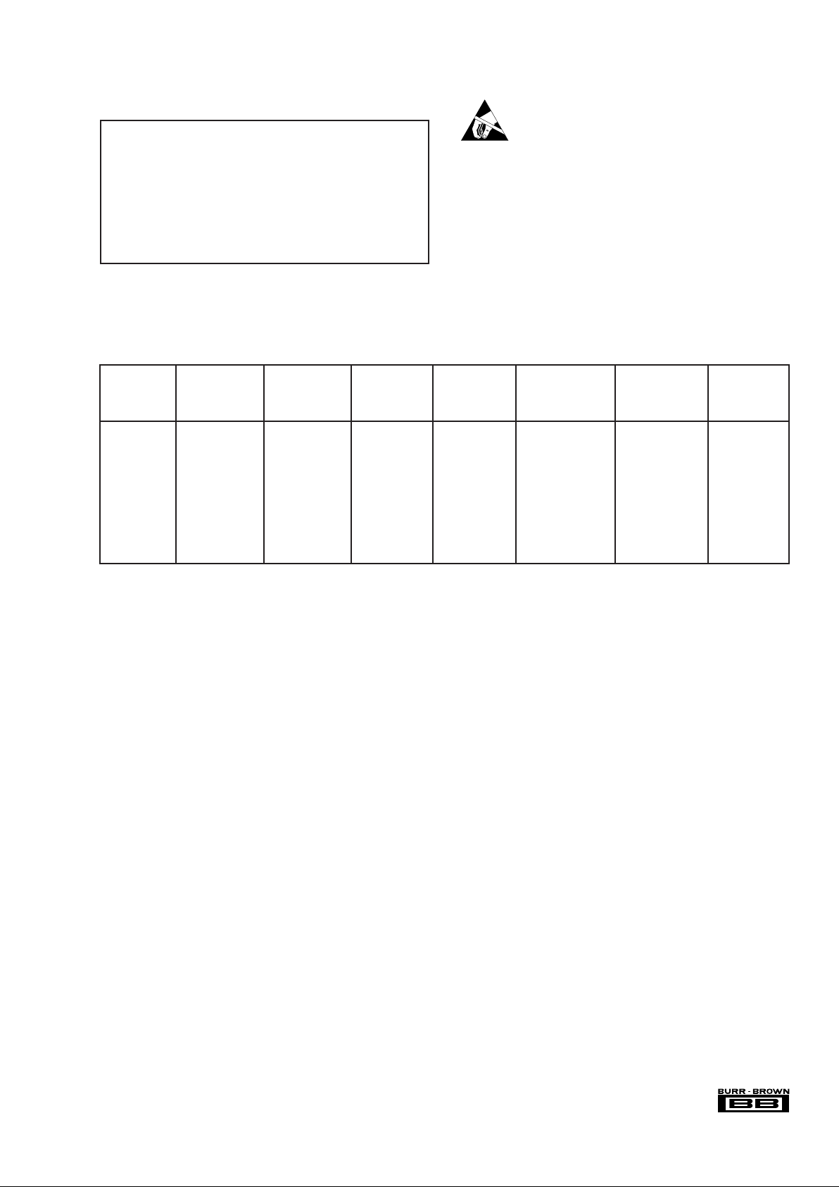
ABSOLUTE MAXIMUM RATINGS
(1)
VDD to VSS........................................................................... –0.3V to +11V
VDD to GND ........................................................................ –0.3V to +5.5V
V
REFL
to VSS...............................................................–0.3V to (VDD – VSS)
VDD to V
REFH
..............................................................–0.3V to (VDD – VSS)
V
REFH
to V
REFL
............................................................–0.3V to (VDD – VSS)
Digital Input Voltage to GND...................................... –0.3V to V
DD
+ 0.3V
Maximum Junction Temperature ................................................... +150°C
Operating Temperature Range ......................................... –40°C to +85°C
Storage Temperature Range .......................................... –65°C to +150°C
Lead Temperature (soldering, 10s) ............................................... +300°C
NOTE: (1) Stresses above those listed under “Absolute Maximum Ratings” may
cause permanent damage to the device. Exposure to absolute maximum
conditions for extended periods may affect device reliability.
ELECTROSTATIC
DISCHARGE SENSITIVITY
This integrated circuit can be damaged by ESD. Burr-Brown
recommends that all integrated circuits be handled with
appropriate precautions. Failure to observe proper handling
and installation procedures can cause damage.
ESD damage can range from subtle performance degradation
to complete device failure. Precision integrated circuits may
be more susceptible to damage because very small parametric
changes could cause the device not to meet its published
specifications.
PACKAGE/ORDERING INFORMATION
MAXIMUM MAXIMUM
LINEARITY DIFFERENTIAL PACKAGE SPECIFICATION
ERROR LINEARITY DRAWING TEMPERATURE ORDERING TRANSPORT
PRODUCT (LSB) (LSB) PACKAGE NUMBER
(1)
RANGE NUMBER
(2)
MEDIA
DAC7614P ±2 ±1 16-Pin DIP 180 –40°C to +85°C DAC7614P Rails
DAC7614PB ±1
""" "DAC7614PB Rails
DAC7614U ±2 ±1 16-Lead SOIC 211 –40°C to +85°C DAC7614U Rails
"" """ "DAC7614U/1K Tape and Reel
DAC7614UB ±1 ±1 16-Lead SOIC 211 –40°C to +85°C DAC7614UB Rails
"" """ "DAC7614UB/1K Tape and Reel
DAC7614E ±2 ±1 20-Lead SSOP 334 –40°C to +85°C DAC7614E Rails
"" """ "DAC7614E/1K Tape and Reel
DAC7614EB ±1 ±1 20-Lead SSOP 334 –40°C to +85°C DAC7614EB Rails
"" """ "DAC7614EB/1K Tape and Reel
NOTES: (1) For detailed drawing and dimension table, please see end of data sheet, or Appendix C of Burr-Brown IC Data Book. (2) Models with a slash (/) are
available only in Tape and Reel in the quantities indicated (e.g., /1K indicates 1000 devices per reel). Ordering 1000 pieces of “DAC7614EB/1K” will get a single
1000-piece Tape and Reel. For detailed Tape and Reel mechanical information, refer to Appendix B of Burr-Brown IC Data Book.
®
4
DAC7614
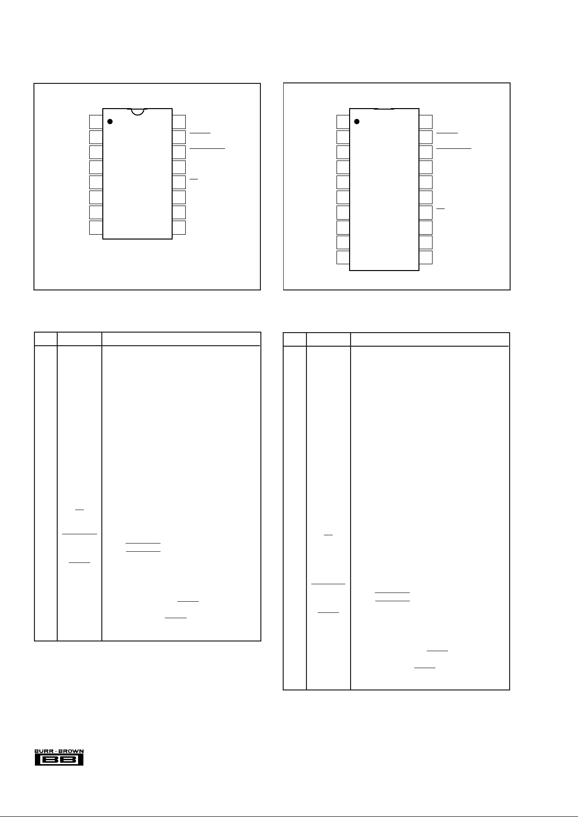
PIN CONFIGURATION—P, U Packages
Top View PDIP, SOIC
PIN DESCRIPTIONS—P, U Packages
PIN LABEL DESCRIPTION
1VDDPositive Analog Supply Voltage, +5V nominal.
2V
OUTD
DAC D Voltage Output
3V
OUTC
DAC C Voltage Output
4V
REFL
Reference Input Voltage Low. Sets minimum output voltage for all DACs.
5V
REFH
Reference Input Voltage High. Sets maximum output voltage for all DACs.
6V
OUTB
DAC B Voltage Output
7V
OUTA
DAC A Voltage Output
8V
SS
Negative Analog Supply Voltage, 0V or –5V nomi-
nal.
9 GND Ground
10 SDI Serial Data Input
11 CLK Serial Data Clock
12 CS Chip Select Input
13 NIC Not Internally Connected.
14 LOADDACS The selected DAC register becomes transparent
when LOADDACS is LOW. It is in the latched state
when LOADDACS is HIGH.
15 RESET Asynchronous Reset Input. Sets all DAC registers
to either zero-scale (000
H
) or mid-scale (800H)
when LOW. RESETSEL determines which code is
active.
16 RESETSEL When LOW, a LOW on RESET will cause all DAC
registers to be set to code 000
H
. When RESETSEL
is HIGH, a LOW on RESET will set the registers to
code 800
H
.
PIN CONFIGURATION—E Package
Top View SSOP
PIN DESCRIPTIONS—E Package
PIN LABEL DESCRIPTION
1VDDPositive Analog Supply Voltage, +5V nominal.
2V
OUTD
DAC D Voltage Output
3V
OUTC
DAC C Voltage Output
4V
REFL
Reference Input Voltage Low. Sets minimum out-
put voltage for all DACs.
5 NIC Not Internally Connected.
6 NIC Not Internally Connected.
7V
REFH
Reference Input Voltage High. Sets maximum out-
put voltage for all DACs.
8V
OUTB
DAC B Voltage Output.
9V
OUTA
DAC A Voltage Output.
10 V
SS
Negative Analog Supply Voltage, 0V or –5V nomi-
nal.
11 GND Ground
12 SDI Serial Data Input
13 CLK Serial Data Clock
14 CS Chip Select Input
15 NIC Not Internally Connected.
16 NIC Not Internally Connected.
17 NIC Not Internally Connected.
18 LOADDACS The selected DAC register becomes transparent
when LOADDACS is LOW. It is in the latched state
when LOADDACS is HIGH.
19 RESET Asynchronous Reset Input. Sets all DAC registers
to either zero-scale (000
H
) or mid-scale (800H)
when LOW. RESETSEL determines which code is
active.
20 RESETSEL When LOW, a LOW on RESET will cause all DAC
registers to be set to code 000
H
. When RESETSEL
is HIGH, a LOW on RESET will set the registers to
code 800
H
.
1
2
3
4
5
6
7
8
16
15
14
13
12
11
10
9
V
DD
V
OUTD
V
OUTC
V
REFL
V
REFH
V
OUTB
V
OUTA
V
SS
RESETSEL
RESET
LOADDACS
NIC
CS
CLK
SDI
GND
DAC7614P, U
1
2
3
4
5
6
7
8
9
10
20
19
18
17
16
15
14
13
12
11
V
DD
V
OUTD
V
OUTC
V
REFL
NIC
NIC
V
REFH
V
OUTB
V
OUTA
V
SS
RESETSEL
RESET
LOADDACS
NIC
NIC
NIC
CS
CLK
SDI
GND
DAC7614E