


Burr Brown Corporation DAC7613EB-1K, DAC7613EB, DAC7613E-1K, DAC7613E Datasheet
1
®
DAC7613
12-Bit, Voltage Output
DIGITAL-TO-ANALOG CONVERTER
®
DAC7613
DESCRIPTION
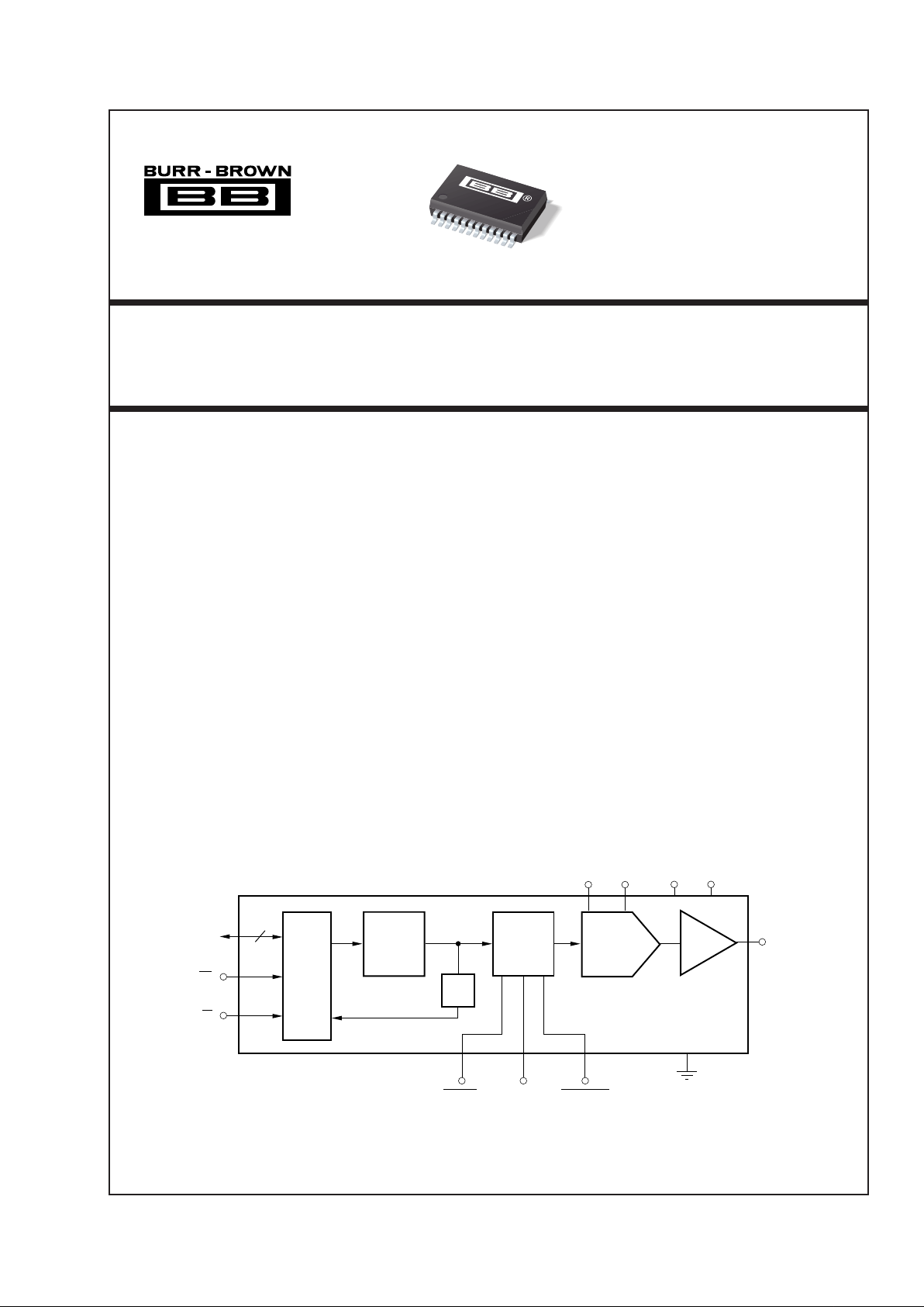
The DAC7613 is a 12-bit, voltage output digital-toanalog converter with guaranteed 12-bit monotonic
performance over the specified temperature range.
The DAC7613 accepts a 12-bit parallel input data, has
double-buffered DAC input logic and provides a
readback mode of the internal input register. An asynchronous reset clears all registers to a mid-scale code
of 800H or to a zero-scale of 000H. The DAC7613 can
operate from a single +5V supply or from +5V and
–5V supplies.
Low power and small size makes the DAC7613 ideal
for data acquisition systems and closed-loop servocontrol. The DAC7613 is available in a plastic
SSOP-24 package, and offers guaranteed specifications over the –40°C to +85°C temperature range.
FEATURES
● LOW POWER: 1.8mW
● UNIPOLAR OR BIPOLAR OPERATION
● SETTLING TIME: 10µs to 0.012%
● 12-BIT LINEARITY AND MONOTONICITY:
–40°C to +85°C
● DATA READBACK
● DOUBLE-BUFFERED DATA INPUTS
● 24-LEAD SSOP PACKAGE
APPLICATIONS
● PROCESS CONTROL
● CLOSED-LOOP SERVO-CONTROL
● MOTOR CONTROL
● DATA ACQUISITION SYSTEMS
© 1998 Burr-Brown Corporation PDS-1500B Printed in U.S.A. January, 2000
International Airport Industrial Park • Mailing Address: PO Box 11400, Tucson, AZ 85734 • Street Address: 6730 S. Tucson Blvd., Tucson, AZ 85706 • Tel: (520) 746-1111
Twx: 910-952-1111 • Internet: http://www.burr-brown.com/ • Cable: BBRCORP • Telex: 066-6491 • FAX: (520) 889-1510 • Immediate Product Info: (800) 548-6132
TS
DAC
Register
DAC
DAC7613
Input
Register
I/O
Buffer
Data I/O
CS
12
R/W
V
REFL
V
OUT
RESET RESETSEL LOADDAC GND
V
REFH
V
DDVSS
DAC7613
For most current data sheet and other product
information, visit www.burr-brown.com
2
®
DAC7613
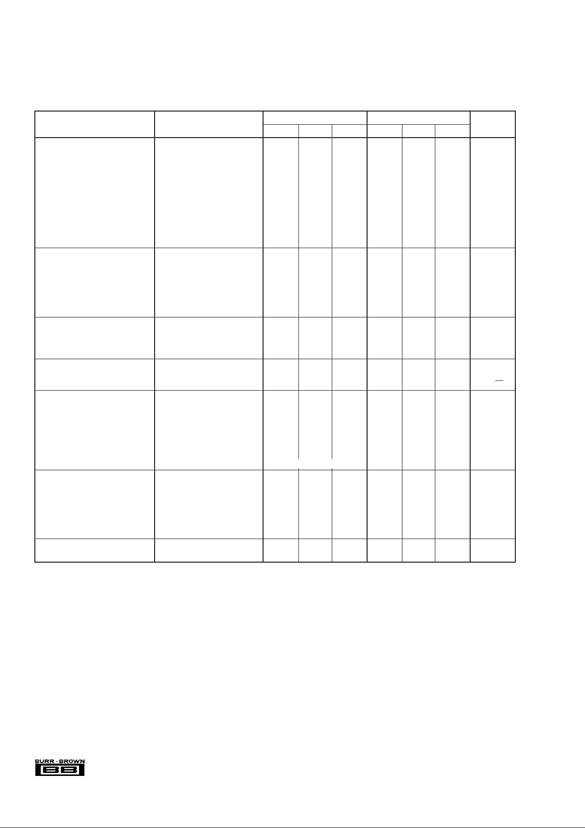
SPECIFICATION
At TA = –40°C to +85°C, VDD = +5V, VSS = –5V, V
REFH
= +2.5V, and V
REFL
= –2.5V, unless otherwise noted.
The information provided herein is believed to be reliable; however, BURR-BROWN assumes no responsibility for inaccuracies or omissions. BURR-BROWN assumes
no responsibility for the use of this information, and all use of such information shall be entirely at the user’s own risk. Prices and specifications are subject to change
without notice. No patent rights or licenses to any of the circuits described herein are implied or granted to any third party. BURR-BROWN does not authorize or warrant
any BURR-BROWN product for use in life support devices and/or systems.
DAC7613E DAC7613EB
NOTES: (1) If VSS = 0V, specification applies at code 00AH and above. (2) LSB means Least Significant Bit, when V
REFH
equals +2.5V and V
REFL
equals –2.5V,
then one LSB equals 1.22mV. (3) Ideal output voltage, does not take into account zero or full-scale error. (4) If V
SS
= –5V, full-scale 5V step. If VSS = 0V, full-scale
positive 2.5V step and negative step from code FFF
H
to 00AH.
PARAMETER CONDITIONS MIN TYP MAX MIN TYP MAX UNITS
ACCURACY
Linearity Error
(1)
VSS = 0V or –5V ±2 ±1 LSB
(2)
Differential Linearity Error VSS = 0V or –5V ±1 ±1 LSB
Monotonicity T
MIN
to T
MAX
12 ✻ Bits
Zero-Scale Error Code = 000
H
±4 ✻ LSB
Zero-Scale Drift 25 ✻✻ppm/°C
Full-Scale Error Code = FFF
H
±4 ✻ LS
Zero-Scale Error Code = 00A
H
, VSS = 0V ±8 ✻ LSB
Zero-Scale Drift VSS = 0V 5 10 ✻✻ppm/°C
Full-Scale Error Code = FFFH, VSS = 0V ±8 ✻ LSB
Power Supply Rejection 30 ✻ ppm/V
ANALOG OUTPUT
Voltage Output
(3)
V
REFL
= 0V, VSS = 0V 0 V
REFH
✻✻V
VSS = –5V V
REFL
V
REFH
✻✻V
Output Current –1.25 +1.25 ✻✻mA
Load Capacitance No Oscillation 100 ✻ pF
Short-Circuit Current +5, –15 ✻ mA
Short-Circuit Duration
Indefinite
✻
REFERENCE INPUT
V
REFH
Input Range VSS = 0V or –5V
V
REFL
+ 1.25
+2.5 ✻✻V
V
REFL
Input Range VSS = 0V 0
V
REFH
– 1.25
✻✻V
V
REFL
Input Range VSS = –5V –2.5
V
REFH
– 1.25
✻✻V
DYNAMIC PERFORMANCE
Settling Time
(4)
To ±0.012% 5 10 ✻✻ µs
Output Noise Voltage 0Hz to 1MHz 40 ✻ nV/√Hz
DIGITAL INPUT/OUTPUT
Logic Family CMOS ✻
Logic Levels
V
IH
IIH ≤ ±10µA 0.7 V
DD
VDD + 0.3 ✻✻V
V
IL
IIL ≤ ±10µA –0.3 0.3 V
DD
✻✻V
V
OH
IOH = –0.8mA 3.6 V
DD
✻✻V
V
OL
IOL = 1.6mA 0.0 0.4 ✻✻V
Data Format Straight Binary ✻
POWER SUPPLY REQUIREMENTS
V
DD
4.75 5.25 ✻✻V
V
SS
If VSS ≠ 0V –5.25 –4.75 ✻✻V
I
DD
0.35 0.5 ✻✻ mA
I
SS
–0.65 –0.45 ✻✻ mA
Power Dissipation V
SS
= –5V 4 5.75 ✻✻ mW
V
SS
= 0V 1.8 2.5 ✻✻ mW
TEMPERATURE RANGE
Specified Performance –40 +85 ✻✻°C
3
®
DAC7613
ABSOLUTE MAXIMUM RATINGS
(1)
V
DD
to VSS............................................................................. –0.3V to 11V
V
DD
to GND .......................................................................... –0.3V to 5.5V
V
REFL
to VSS..............................................................–0.3V to (V
DD
– VSS)
V
DD
to V
REFH
............................................................. –0.3V to (V
DD
– VSS)
V
REFH
to V
REFL
..........................................................–0.3V to (V
DD
– VSS)
Digital Input Voltage to GND ................................... –0.3V to V
DD
+ 0.3V
Digital Output Voltage to GND ................................. –0.3V to V
DD
+ 0.3V
Maximum Junction Temperature................................................... +150°C
Operating Temperature Range ........................................ –40°C to +85°C
Storage Temperature Range ......................................... –65°C to +150°C
Lead Temperature (soldering, 10s) ............................................... +300°C
NOTE: (1) Stresses above those listed under “Absolute Maximum Ratings”
may cause permanent damage to the device. Exposure to absolute maximum
conditions for extended periods may affect device reliability.
ELECTROSTATIC
DISCHARGE SENSITIVITY
This integrated circuit can be damaged by ESD. Burr-Brown
recommends that all integrated circuits be handled with
appropriate precautions. Failure to observe proper handling
and installation procedures can cause damage.
ESD damage can range from subtle performance degradation
to complete device failure. Precision integrated circuits may
be more susceptible to damage because very small parametric
changes could cause the device not to meet its published
specifications.
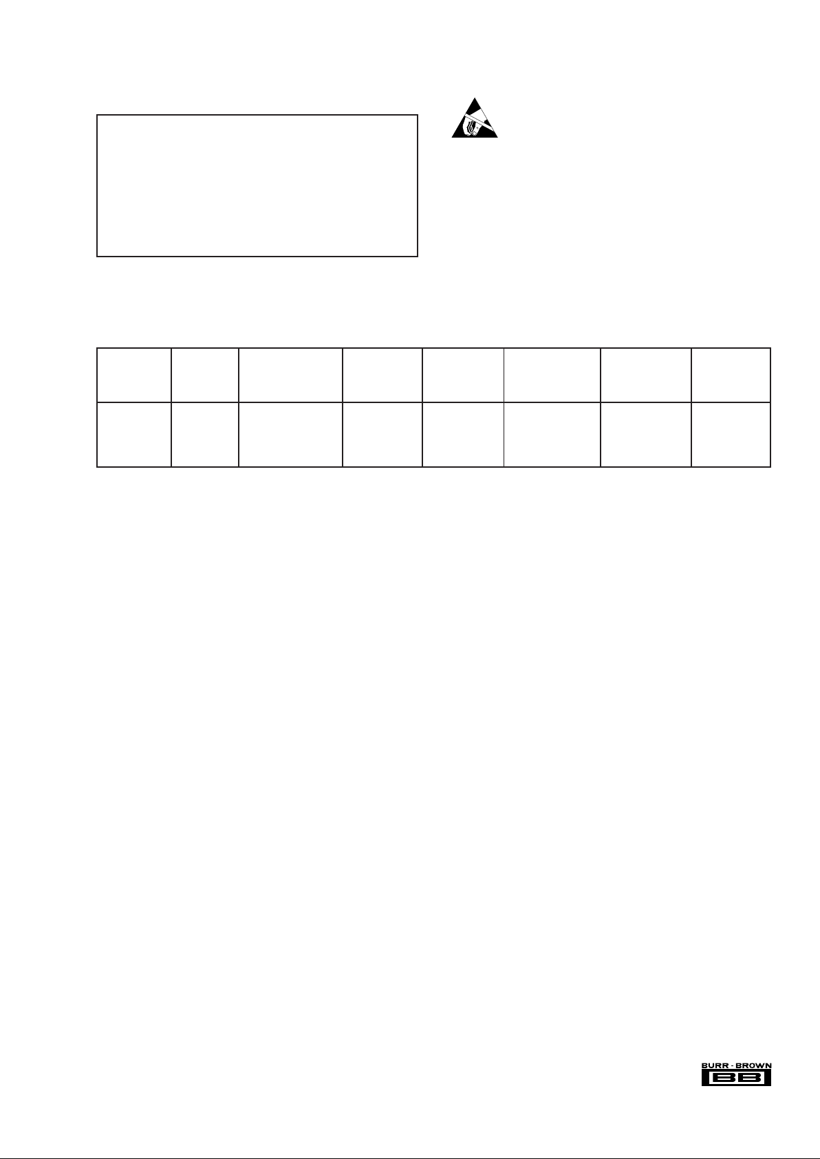
PACKAGE/ORDERING INFORMATION
MAXIMUM MAXIMUM
LINEARITY DIFFERENTIAL PACKAGE SPECIFICATION
ERROR LINEARITY ERROR DRAWING TEMPERATURE ORDERING TRANSPORT
PRODUCT (LSB) (LSB) PACKAGE NUMBER RANGE NUMBER
(1)
MEDIA
DAC7613E ±2 ±1 SSOP-24 338 –40°C to +85°C DAC7613E Rails
""""""DAC7613E/1K Tape and Reel
DAC7613EB ±1 ±1 SSOP-24 338 –40°C to +85°C DAC7613EB Rails
""""""DAC7613EB/1K Tape and Reel
NOTE: (1) Models with a slash (/) are available only in Tape and Reel in the quantities indicated (e.g., /1K indicates 1000 devices per reel). Ordering 1000 pieces
of “DAC7613E/1K” will get a single 1000-piece Tape and Reel.