

Burr Brown Corporation DAC725KP, DAC725JP Datasheet
®
DAC725
Dual 16-Bit
DIGITAL-TO-ANALOG CONVERTER
FEATURES
● COMPLETE DUAL V
● DOUBLE-BUFFERED INPUT REGISTER
● HIGH-SPEED DATA INPUT:
Serial or Parallel
● HIGH ACCURACY:
● 14-BIT MONOTONICITY OVER
TEMPERATURE
● PLASTIC PACKAGE
● CLEAR INPUT TO SET ZERO OUTPUT
DAC
OUT
±0.003% Linearity Error
High
Byte
Low
Byte
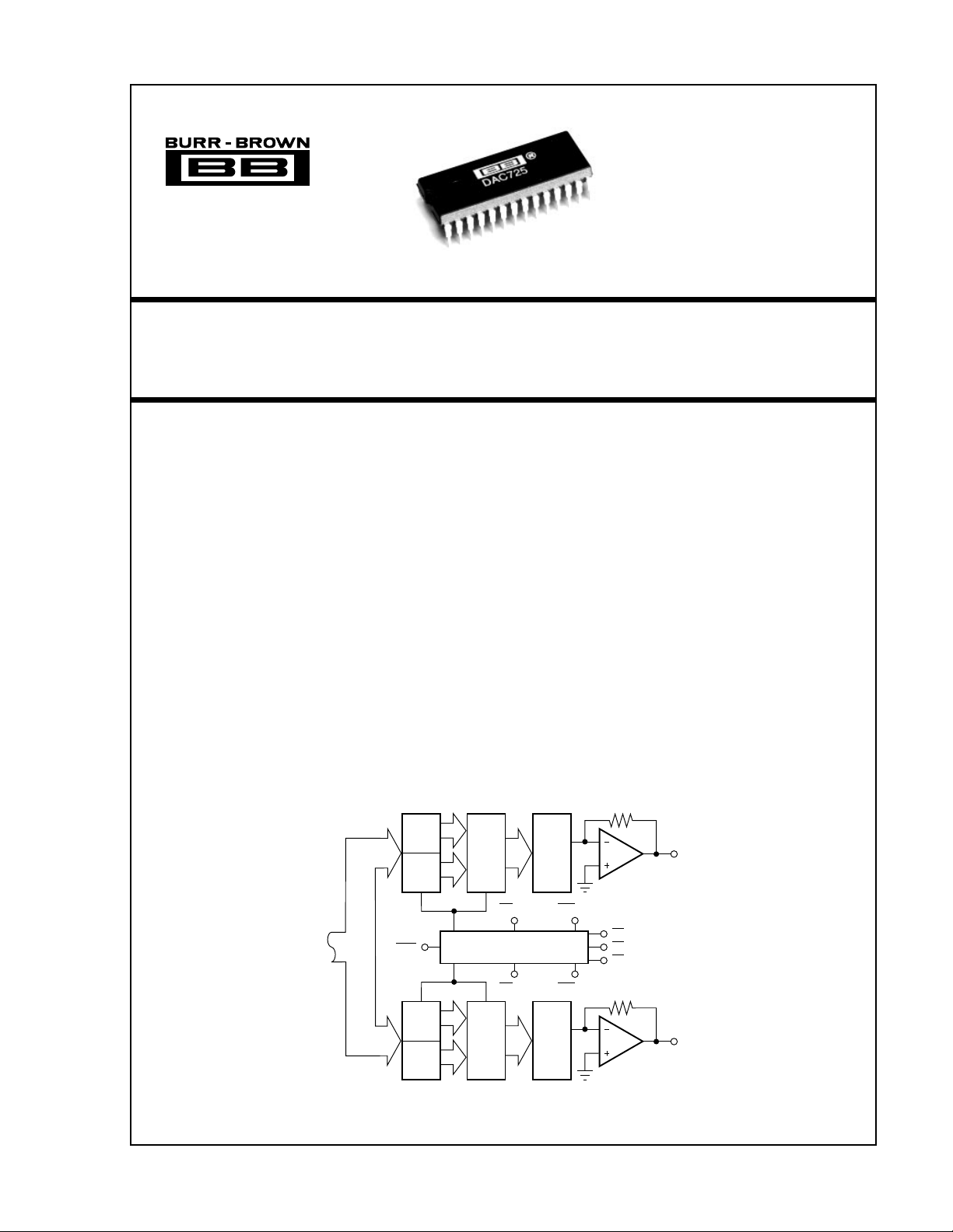
DESCRIPTION
The DAC725 is a dual 16-bit DAC, complete with
internal reference and output op amps. The DAC725 is
designed to interface to an 8-bit microprocessor bus,
but can also be interfaced to wider buses. The hybrid
construction minimizes the digital feedthrough typically associated with products that combine the digital
bus interface circuitry with high-accuracy analog circuitry.
The 16-bit data word is loaded into either of the DACs
in two 8-bit bytes per 16-bit word. The versatility of
the control lines allows the data word to be directed to
either DAC, in any order. The voltage-out DACs are
dedicated to a bipolar output voltage of ±10V. The
output is immediately set to 0V when the Clear command is given. This feature, combined with the bus
interfacing and complete DAC circuitry, makes the
DAC725 ideal for automatic test equipment, power
control, servo systems, and robotics applications.
8
D/A
Latch
8
16-
Bit
16
D/A
(A)
CS (A) WR (A)
A
8-Bit
Data Bus
International Airport Industrial Park • Mailing Address: PO Box 11400 • Tucson, AZ 85734 • Street Address: 6730 S. Tucson Blvd. • Tucson, AZ 85706
Tel: (520) 746-1111 • Twx: 910-952-1111 • Cable: BBRCORP • Telex: 066-6491 • FAX: (520) 889-1510 • Immediate Product Info: (800) 548-6132
© 1987 Burr-Brown Corporation PDS-757D Printed in U.S.A. August, 1993
CLR
High
Byte
Low
Byte
8
8
Control Logic
CS (B) WR (B)
D/A
16
Latch
16-
Bit
D/A
(B)
0
A
1
A
2
SPECIFICATIONS
ELECTRICAL
At TA = +25°C, V
PARAMETER MIN TYP MAX MIN TYP MAX UNITS
INPUT
DIGITAL INPUT
Resolution 16 * Bits
Bipolar Input Code Binary Twos Complement *
Logic Levels
TRANSFER CHARACTERISTICS
ACCURACY
Linearity Error ±0.003 ±0.006 ±0.0015 ±0.003 % of FSR
Differential Linearity Error
At Bipolar Zero: KP
Gain Error
Bipolar Zero Error
Montonicity Over Specified Temp. Range 13 14 Bits
Power Supply Sensitivity: +V
DRIFT (Over Specified Temperature Range)
Gain Drift ±10 * ±25 ppm/°C
Bipolar Zero Drift ±5*±12 ppm of FSR/°C
Differential Linearity Over Temperature
Linearity Error Over Temperature
SETTLING TIME (to ±0.003% of FSR)
20V Step (2kΩ load) 4 * 8 µs
1LSB Step at Worst-Case Code
Slew Rate 10 * V/µs
OUTPUT
Output Voltage Range
Output Current ±5* mA
Output Impedance 0.15 * Ω
Short Circuit to Common Duration Indefinite *
POWER SUPPLY REQUIREMENTS
Voltage: +V
Current (No load, ±15V supplies): +V
Power Dissipation (±15V supplies) 920 1175 * * mW
TEMPERATURE RANGE
Specification 0 +70 * * °C
Storage –60 +150 * * °C
*Specification same as model to the left.
NOTES: (1) Digital inputs are TTL, LSTTL, 54/74HC and 54/74HTC compatible over the specification temperature range. (2) FSR means Full-Scale Range. For
example, for ±10V output, FSR = 20V. (3) ±0.0015% of FSR is equal to 1LSB in 16-bit resolution. ±0.003% of FSR is equal to 1LSB in 15-bit resolution. ±0.006%
of FSR is equal to 1LSB in 14-bit resolution. (4) Error at input code 0000
potentiometer rotates the transfer function around the bipolar zero point. (6) Maximum represents the 3σ limit. Not tested for this parameter. (7) The bipolar worstcase code change is FFFF
±9V.
= ±15V, and after a 10-minute warm-up unless otherwise noted.
CC
DAC725JP DAC725KP
(1)
:V
IH
V
IL
I
(VI = +2.7V) 1 * µA
IH
I
(VI = +0.4V) 1 * µA
IL
(3)
(3, 4)
(5)
, –V
CC
CC
V
DD
(3)
(3)
(6)
(7)
(8)
CC
CC
CC
–V
CC
V
DD
to 0000H (BTC). (8) Minimum supply voltage for ±10V output swing is approximately ±13V. Output swing for ±12V supplies is at least
H
–V
V
(5)
DD
+2 +5.5 * * V
–1 +0.8 * * V
±0.0045 ±0.012 0.003 ± 0.006 % of FSR
±0.003 ±0.006 % of FSR
±0.07 ±0.2 * ±0.15 %
±0.05 ±0.1 * * % of FSR
±0.0015 ±0.006 * * % of FSR/%V
±0.0001 ±0.001 * * % of FSR/%V
±0.0045 ±0.012 ±0.003 ±0.006 % of FSR
±0.012 ±0.006 % of FSR
2.5 * 4 µs
±10 * V
+11.4 +15 +16.5 * * * V
–11.4 –15 –16.5 * * * V
+4.5 +5 +5.5 * * * V
+29 +35 * * mA
–35 –40 * * mA
+6 +10 * * mA
(BTC). (5) Adjustable to zero with external trim potentiometer. Adjusting the gain
H
(2)
CC
DD
The information provided herein is believed to be reliable; however, BURR-BROWN assumes no responsibility for inaccuracies or omissions. BURR-BROWN assumes
no responsibility for the use of this information, and all use of such information shall be entirely at the user’s own risk. Prices and specifications are subject to change
without notice. No patent rights or licenses to any of the circuits described herein are implied or granted to any third party. BURR-BROWN does not authorize or warrant
any BURR-BROWN product for use in life support devices and/or systems.
®
DAC725
2
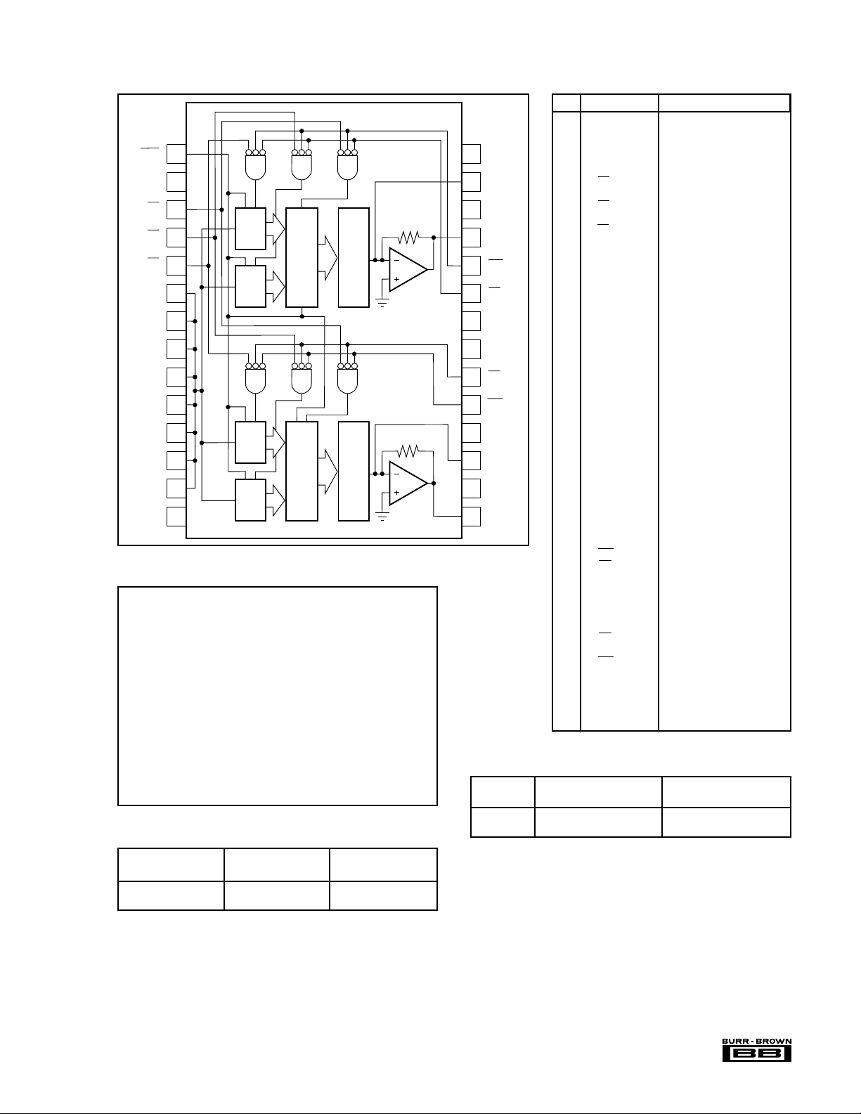
CONNECTION DIAGRAM
1
CLR
V
2
DD
A
3
D
7
D
6
D
5
D
4
D
3
D
2
D
1
D
0
DCOM
2
A
4
0
A
5
1
6
(D
)
15
7
(D
)
14
8
(D
)
13
9
(D
)
12
10
(D
)
11
11
(D
)
10
12
)
(D
9
13
)
(D
8
14
High
Byte
Latch
Low
Byte
Latch
High
Byte
Latch
Low
Byte
Latch
8
D/A
Latch
16-
16
Bit
D/A
8
8
D/A
Latch
16-
16
Bit
D/A
8
ABSOLUTE MAXIMUM RATINGS
VDD to COMMON ........................................................................ 0V, +15V
+V
to COMMON ...................................................................... 0V, +18V
CC
–V
to COMMON ...................................................................... 0V, –18V
CC
Digital Data Inputs to COMMON...................................... –0.5V, V
DC Current any Input ...................................................................... ±10mA
DD
Reference Out to COMMON ........................ Indefinite Short to COMMON
V
............................................................ Indefinite Short to COMMON
OUT
External Voltage Applied to R
External Voltage Applied to D/A Output ............................................... ±5V
......................................................... ±18V
F
Power Dissipation ........................................................................ 2000mW
Storage Temperature...................................................... –60°C to +150°C
Lead Temperature (soldering, 10s).................................................. 300°C
NOTE: These devices are sensitive to electrostatic discharge. Appropriate
I.C. handling procedures should be followed.
Stresses above those listed under “Absolute Maximum Ratings” may cause
permanent damage to the device. Exposure to absolute maximum conditions for extended periods may affect device reliability.
ORDERING INFORMATION
MODEL max (% of FSR) RANGE
DAC725JP ±0.012 0°C to +70°C
DAC725KP ±0.006 0°C to +70°C
LINEARITY ERROR TEMPERATURE
+ 0.5
PIN DESCRIPTIONS
PIN DESIGNATOR DESCRIPTION
1 CLR Clear line. Sets the D/A
register to 0000
28
GA (A)
2V
27
SJ (A)
ACOM
26
(A)
25
(A)
V
OUT
3A
4A
5A
6D
24
WR (A)
DD
2
0
1
(D15) Input for data bit 7 if en-
7
(MSB) abling low byte (LB) latch,
which gives bipolar zero
on the D/A output.
Logic supply (+5V).
Latch enable for D/A latch
(active low).
Latch enable for “low byte”
input (active low).
Latch enable for “high byte”
input (active low).
HEX
,
or data bit 15 if enabling
23
CS (A)
22
–V
CC
7D
(D14) Input for data bit 6 if en-
6
the high byte (HB) latch.
abling LB latch, or data bit
14 if enabling HB latch.
8D5 (D13) Data bit 5 (LB) or data bit
21
+V
CC
20
CS (B)
19
WR (B)
18
GA (B)
17
SJ (B)
ACOM
16
(B)
15
(B)
V
OUT
9D
10 D
11 D
12 D
13 D
(D12) Data bit 4 (LB) or data bit
4
(D11) Data bit 3 (LB) or data bit
3
(D10) Data bit 2 (LB) or data bit
2
(D9) Data bit 1 (LB) or data bit 9
1
(D8) Data bit 0 (LB) or data bit
0
14 DCOM Digital common.
15 V
16 ACOM (B)
(B) Voltage output for DAC B.
OUT
17 SJ (B) Summing junction of the in-
13 (HB).
12 (HB).
11 (HB).
10 (HB).
(HB).
8 (HB).
Analog common for DAC B.
ternal op amp for DAC B.
18 GA (B) Gain adjust pin for DAC B.
19 WR (B)
Write control line for DAC B.
20 CS (B) Chip select control line for
DAC B.
21 +V
22 –V
CC
CC
Positive supply voltage
(+15V).
Negative supply voltage
(–15V).
23 CS (A) Chip select control line for
DAC A.
24 WR (A)
25 V
26 ACOM (A) Analog common for DAC A.
(A) Voltage output for DAC A.
OUT
Write control line for DAC A.
27 SJ (A) Summing junction of the in-
ternal op amp for DAC A.
28 GA (A) Gain adjust pin for DAC A.
PACKAGE INFORMATION
MODEL PACKAGE NUMBER
PACKAGE DRAWING
DAC725JP 28-Pin Plastic DIP 215
DAC725KP 28-Pin Plastic DIP 215
NOTE: (1) For detailed drawing and dimension table, please see end of data
sheet, or Appendix D of Burr-Brown IC Data Book.
(1)
®
3
DAC725
 Loading...