

Burr Brown Corporation DAC714U, DAC714P, DAC714HL, DAC714HC, DAC714HB Datasheet
®
DAC714
16-Bit DIGITAL-TO-ANALOG CONVERTER
With Serial Data Interface
FEATURES:
● SERIAL DIGITAL INTERFACE
● VOLTAGE OUTPUT:
●
±1 LSB INTEGRAL LINEARITY
16-BIT MONOTONIC OVER TEMPERATURE
●
● PRECISION INTERNAL REFERENCE
● LOW NOISE: 120nV/ √Hz Including Reference
● 16-LEAD PLASTIC AND CERAMIC SKINNY
DIP AND PLASTIC SOIC PACKAGES
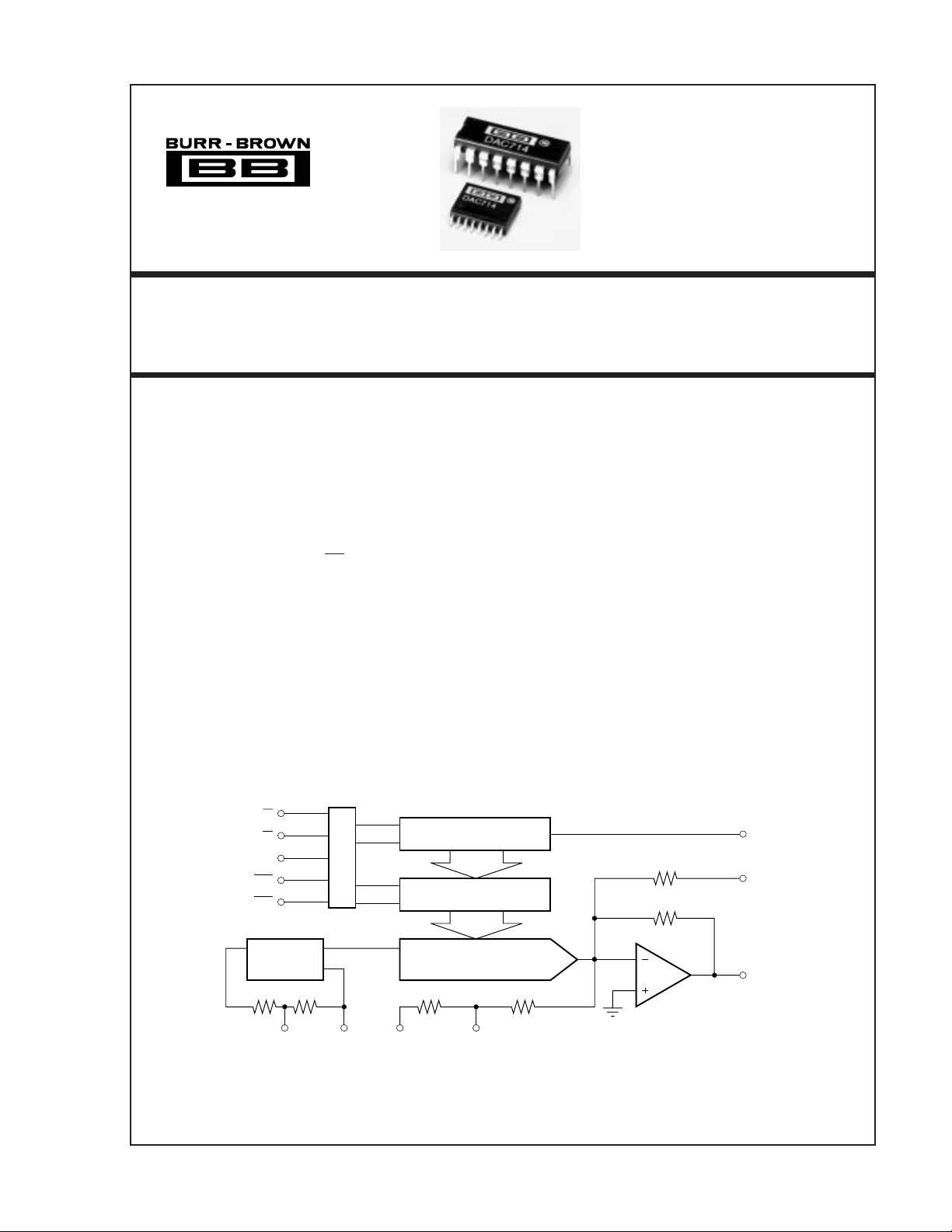
A
0
A
1
SDI
CLK
CLR
±10V, ±5V, 0 to +10V
Input Shift Register
D/A Latch
DESCRIPTION
The DAC714 is a complete monolithic digital-toanalog converter including a +10V temperature compensated reference, current-to-voltage amplifier, a
high-speed synchronous serial interface, a serial output which allows cascading multiple converters, and
an asynchronous clear function which immediately
sets the output voltage to midscale.
The output voltage range is ±10V, ±5V, or 0 to +10V
while operating from ±12V or ±15V supplies. The
gain and bipolar offset adjustments are designed so
that they can be set via external potentiometers or
external D/A converters. The output amplifier is protected against short circuit to ground.
The 16-pin DAC714 is available in a plastic 0.3" DIP,
ceramic 0.3" CERDIP, and wide-body plastic SOIC
package. The DAC714P, U, HB, and HC are specified
over the –40°C to +85°C temperature range while the
DAC714HL is specified over the 0°C to +70°C range.
SDO
16
R
FB2
16
Reference
Circuit
V
REF OUT
Adjust
International Airport Industrial Park • Mailing Address: PO Box 11400, Tucson, AZ 85734 • Street Address: 6730 S. Tucson Blvd., Tucson, AZ 85706 • Tel: (520) 746-1111 • Twx: 910-952-1111
Internet: http://www.burr-brown.com/ • FAXLine: (800) 548-6133 (US/Canada Only) • Cable: BBRCORP • Telex: 066-6491 • FAX: (520) 889-1510 • Immediate Product Info: (800) 548-6132
© 1994 Burr-Brown Corporation PDS-1252D Printed in U.S.A. July, 1997
+10V
16-Bit D/A Converter
R
BPO
V
OUT
Offset AdjustGain
®
1
DAC714
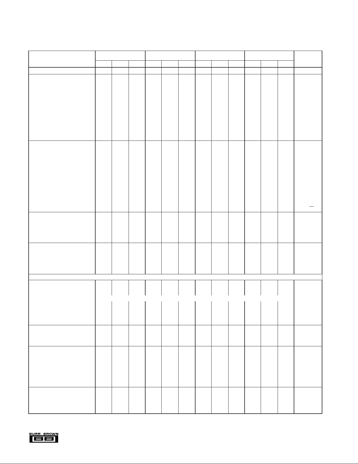
SPECIFICATIONS
At TA = +25°C, +V
PARAMETER MIN TYP MAX MIN TYP MAX MIN TYP MAX MIN TYP MAX UNITS
TRANSFER CHARACTERISTICS
ACCURACY
Linearity Error ±4 ±2 ±1 ±1 LSB
T
to T
MIN
MAX
Differential Linearity Error ±4 ±2 ±1 ±1 LSB
T
to T
MIN
MAX
Monotonicity 14 15 16 16 Bits
Monotonicity Over Spec Temp Range 13 14 15 16 Bits
Gain Error
T
to T
MIN
MAX
Unipolar/Bipolar Zero Error
T
to T
MIN
MAX
Power Supply Sensitivity of Gain ±0.003 ±0.003 ±0.003 ±0.003 %FSR/%V
DYNAMIC PERFORMANCE
Settling Time
(to ±0.003%FSR, 5kΩ || 500pF Load)
20V Output Step 6 10 6 10 6 10 6 10 µs
1LSB Output Step
Output Slew Rate 10 10 10 10 V/µs
Total Harmonic Distortion
0dB, 1001Hz, f
–20dB, 1001Hz, f
–60dB, 1001Hz, f
SINAD: 1001Hz, f
Digital Feedthrough
Digital-to-Analog Glitch Impulse
Output Noise Voltage (includes reference)
ANALOG OUTPUT
Output Voltage Range
+V
, –VCC = ±11.4V ±10 ±10 ±10 ±10 V
CC
Output Current ±5 ±5 ±5 ±5mA
Output Impedance 0.1 0.1 0.1 0.1 Ω
Short Circuit to ACOM Duration Indefinite Indefinite Indefinite Indefinite
REFERENCE VOLTAGE
Voltage +9.975 +10.000 +10.025 +9.975 +10.000 +10.025 +9.975 +10.000 +10.025 +9.975 +10.000 +10.025 V
T
to T
MIN
MAX
Output Resistance 1 1 1 1 Ω
Source Current 2 2 2 2 mA
Short Circuit to ACOM Duration Indefinite Indefinite Indefinite Indefinite
INTERFACE
RESOLUTION 16 16 16 16 Bits
DIGITAL INPUTS
Serial Data Input Code
Logic Levels
V
IH
V
IL
(VI = +2.7V) ±10 ±10 ±10 ±10 µA
I
IH
(VI = +0.4V) ±10 ±10 ±10 ±10 µA
I
IL
DIGITAL OUTPUT
Serial Data
V
OL (ISINK
V
OH (ISOURCE
POWER SUPPLY REQUIREMENTS
Voltage
+V
CC
–V
CC
Current (No Load, ±15V Supplies)
+V
CC
–V
CC
Power Dissipation
TEMPERATURE RANGES
Specification
All Grades –40 +85 –40 +85 –40 +85 0 +70 °C
Storage –60 +150 –60 +150 –60 +150 –60 +150 °C
Thermal Coefficient,
NOTES: (1) Digital inputs are TTL and +5V CMOS compatible over the specification temperature range. (2) FSR means Full Scale Range. For example, for ±10V output, FSR = 20V. (3) Errors
externally adjustable to zero. (4) Maximum represents the 3σ limit. Not 100% tested for this parameter. (5) For the worst-case Binary Two’s Complement code changes: FFFF
to FFFFH. (6) During power supply turn on, the transient supply current may approach 3x the maximum quiescent specification. (7) Typical (i.e. rated) supply voltages times maximum currents.
= +12V and +15V, –VCC = –12V, and –15V, unless otherwise noted.
CC
DAC714P, U DAC714HB DAC714HC DAC714HL
±8 ±4 ±2 ±2 LSB
±8 ±4 ±2 ±1 LSB
(3)
(3)
±0.1 ±0.1 ±0.1 ±0.1 %
±0.25 ±0.25 ±0.25 ±0.25 %
±0.1 ±0.1 ±0.1 ±0.1 % of FSR
±0.2 ±0.2 ±0.2 ±0.2 % of FSR
±30 ±30 ±30 ±30 ppm FSR/%V
(4)
(5)
= 100kHz 0.005 0.005 0.005 0.005 %
S
= 100kHz 0.03 0.03 0.03 0.03 %
S
= 100kHz 3.0 3.0 3.0 3.0 %
S
= 100kHz 87 87 87 87 dB
S
(5)
(5)
4444µs
2 2 2 2 nV–s
15 15 15 15 nV–s
120 120 120 120 nV/√Hz
+9.960 +10.040 +9.960 +10.040 +9.960 +10.040 +9.960 +10.040 V
(1)
+2.0
(VCC –1.4)
+2.0
Binary Two’s Complement
(VCC –1.4)
+2.0
(VCC –1.4)
+2.0
(VCC –1.4)
0 +0.8 0 +0.8 0 +0.8 0 +0.8 V
= 1.6mA) 0 +0.4 0 +0.4 0 +0.4 0 +0.4 V
= 500µA), T
MIN
to T
+2.4 +5 +2.4 +5 +2.4 +5 +2.4 +5 V
MAX
+11.4 +15 +16.5 +11.4 +15 +16.5 +11.4 +15 +16.5 +11.4 +15 +16.5 V
–11.4 –15 –16.5 –11.4 –15 –16.5 –11.4 –15 –16.5 –11.4 –15 –16.5 V
(6)
13 16 13 16 13 16 13 16 mA
(7)
θ
JA
®
DAC714
22 26 22 26 22 26 22 26 mA
625 625 625 625 mW
75 75 75 75 °C/W
to 0000H and 0000
H
2
(2)
CC
CC
V
H
PIN CONFIGURATION
Top View
1
CLK
2
A
0
3
A
1
4
SDI
5
SDO
6
DCOM
7
+V
CC
8
ACOM
DAC714
16
CLR
15
–V
14
Gain Adjust
13
Offset Adjust
12
V
11
R
10
R
9
V
CC
REF OUT
BPO
FB2
OUT
SOIC/DIP
PIN DESCRIPTIONS
PIN LABEL DESCRIPTION
1 CLK Serial Data Clock
2A
3A
4 SDI Serial Data Input
5 SDO Serial Data Output
6 DCOM Digital Ground
7+V
8 ACOM Analog Ground
9V
10 R
11 R
12 V
13 Offset Adjust Offset Adjust
14 Gain Adjust Gain Adjust
15 –V
16 CLR Clear
0
1
CC
OUT
FB2
BPO
REF OUT
CC
Enable for Input Register (Active Low)
Enable for D/A Latch (Active Low)
Positive Power Supply
D/A Output
±10V Range Feedback Output
Bipolar Offset
Voltage Reference Output
Negative Power Supply
ELECTROSTATIC
DISCHARGE SENSITIVITY
Electrostatic discharge can cause damage ranging from performance degradation to complete device failure. BurrBrown Corporation recommends that all integrated circuits
be handled and stored using appropriate ESD protection
methods.
ESD damage can range from subtle performance degradation to complete device failure. Precision integrated circuits
may be more susceptible to damage because very small
parametric changes could cause the device not to meet
published specifications.
ABSOLUTE MAXIMUM RATINGS
to Common .................................................................... 0V to +17V
+V
CC
–V
to Common .................................................................... 0V to –17V
CC
+V
to –VCC....................................................................................... 34V
CC
ACOM to DCOM ............................................................................... ±0.5V
Digital Inputs to Common............................................. –1V to (V
External Voltage Applied to BPO and Range Resistors..................... ±V
V
......................................................... Indefinite Short to Common
REF OUT
V
............................................................... Indefinite Short to Common
OUT
SDO ............................................................... Indefinite Short to Common
Power Dissipation .......................................................................... 750mW
Storage Temperature ...................................................... –60°C to +150°C
Lead Temperature (soldering, 10s)................................................ +300°C
NOTE: (1) Stresses above those listed under “Absolute Maximum Ratings”
may cause permanent damage to the device. Exposure to absolute maximum
conditions for extended periods may affect device reliability.
(1)
CC
–0.7V)
CC
ORDERING INFORMATION
PRODUCT PACKAGE max at +25
DAC714P Plastic DIP ±4 LSB –40°C to +85°C
DAC714U Plastic SOIC ±4 LSB –40°C to +85°C
DAC714HB Ceramic DIP ±2 LSB –40°C to +85°C
DAC714HC Ceramic DIP ±1 LSB –40°C to +85°C
DAC714HL Ceramic DIP ±1 LSB 0°C to +70°C
LINEARITY ERROR TEMPERATURE
°C RANGE
PACKAGE INFORMATION
PRODUCT PACKAGE NUMBER
PACKAGE DRAWING
DAC714P Plastic DIP 180
DAC714U Plastic SOIC 211
DAC714H Ceramic DIP 129
NOTE: (1) For detailed drawing and dimension table, please see end of data sheet,
or Appendix C of Burr-Brown IC Data Book.
(1)
The information provided herein is believed to be reliable; however, BURR-BROWN assumes no responsibility for inaccuracies or omissions. BURR-BROWN assumes
no responsibility for the use of this information, and all use of such information shall be entirely at the user’s own risk. Prices and specifications are subject to change
without notice. No patent rights or licenses to any of the circuits described herein are implied or granted to any third party. BURR-BROWN does not authorize or warrant
any BURR-BROWN product for use in life support devices and/or systems.
3
DAC714
®
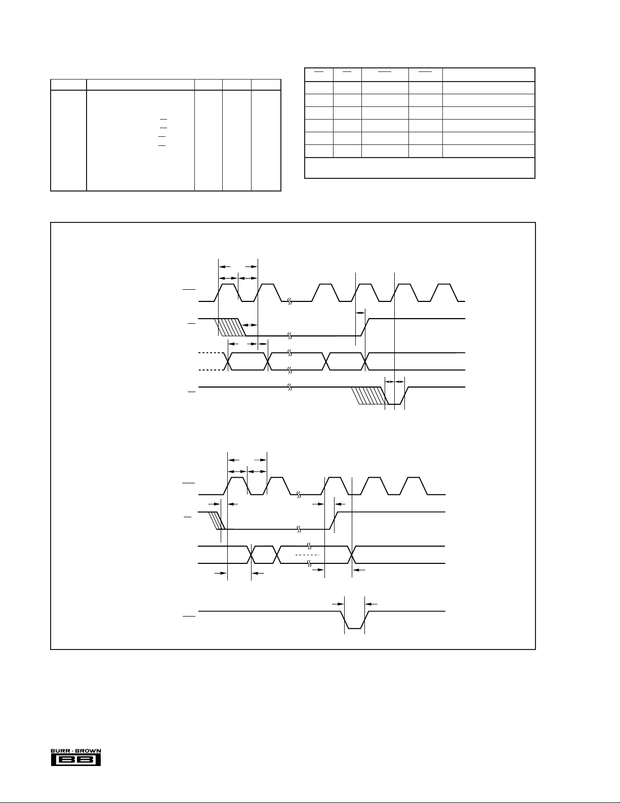
TIMING SPECIFICATIONS
TA = –40°C to +85°C, +VCC = +12V or +15V, –VCC = –12V or –15V.
SYMBOL PARAMETER MIN MAX UNITS
t
CLK
t
CL
t
CH
t
A0S
t
A1S
t
AOH
t
A1H
t
DS
t
DH
t
DSOP
t
CP
Data Clock Period 100 ns
Clock LOW 50 ns
Clock HIGH 50 ns
Setup Time for A
Setup Time for A
Hold Time for A
Hold Time for A
Setup Time for DATA 50 ns
0
1
0
1
50 ns
50 ns
0ns
0ns
Hold Time for DATA 10 ns
Output Propagation Delay 140 ns
Clear Pulsewidth 200 ns
TIMING DIAGRAMS
Serial Data In
t
CLK
Serial Data Input
MSB First
Latch Data
In D/A Latch
CLK
SDI
t
CH
A
0
A
1
t
CL
t
A0S
t
DS
D
15
TRUTH TABLE
A
A
0
011 → 0 → 1 1 Shift Serial Data into SDI
101 → 0 → 1 1 Load D/A Latch
111 → 0 → 1 1 No Change
001 → 0 → 1 1 Two Wire Operation
X X 1 1 No Change
X X X 0 Reset D/A Latch
NOTES: X = Don’t Care. (1) All digital input changes will appear at the
output.
t
A0H
t
DH
D
14
D
0
CLK CLR DESCRIPTION
1
t
A1S
t
A1H
(1)
Serial Data
Out
CLK
A
SDO
CLR
Serial Data Out
t
CLK
t
CH
0
t
DSOP
t
CL
t
A0S
D
15
D
14
Clear
t
A0H
D
0
t
DSOP
t
CP
®
DAC714
4
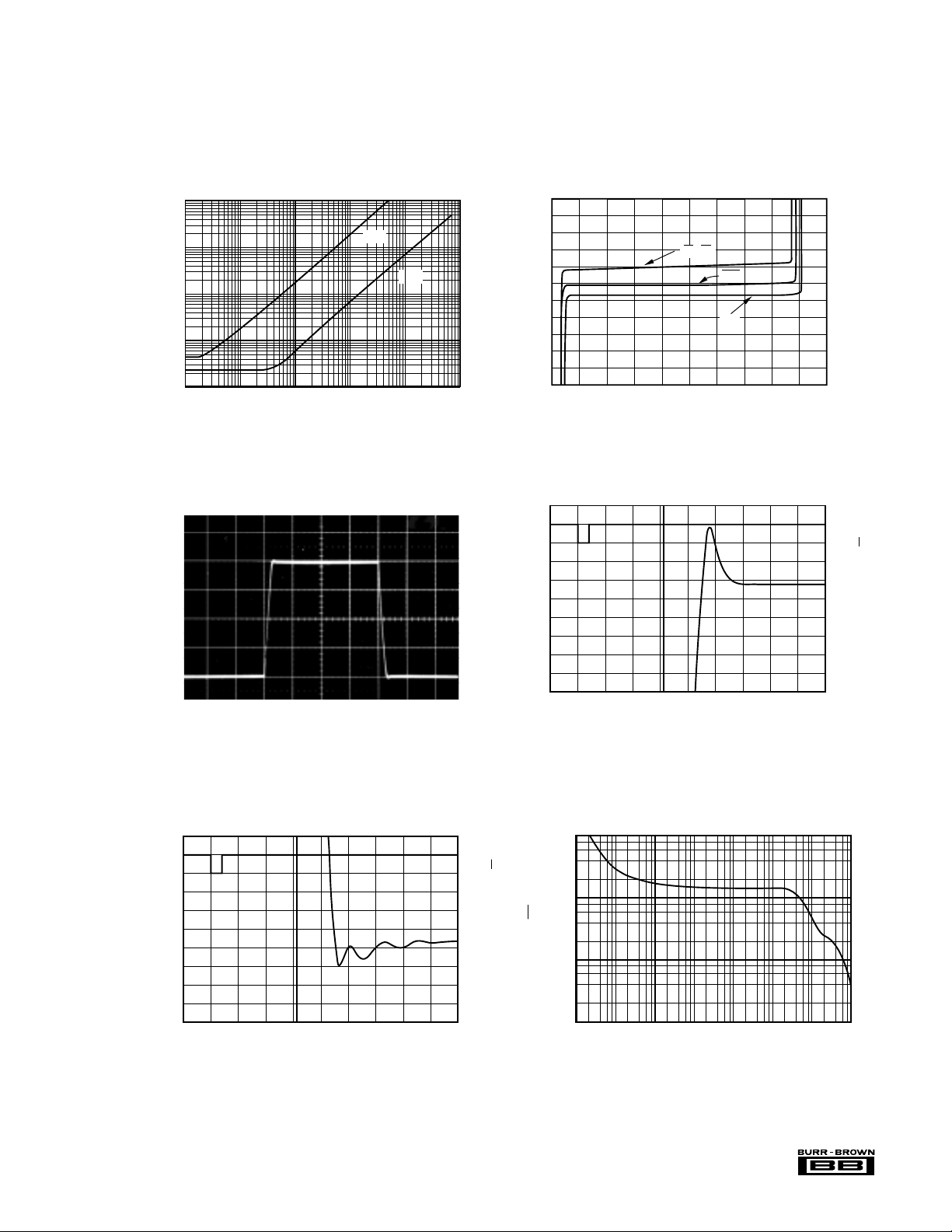
TYPICAL PERFORMANCE CURVES
1000
100
10
1
1 10 100 1k 10k 100k 1M 10M
Frequency (Hz)
nV/√Hz
V
OUT
SPECTRAL NOISE DENSITY
At TA = +25°C, VCC = ±15V, unless otherwise noted.
POWER SUPPLY REJECTION vs
POWER SUPPLY RIPPLE FREQUENCY
1k
–V
100
10
(ppm of FSR/ %)
1
0.1
[Change in FSR]/[Change in Supply Voltage]
10 100 1k 10k 100k 1M
Frequency (Hz)
± FULL SCALE OUTPUT SWING
10
OUT
0
V (V)
–10
Time (10µs/div)
LOGIC vs V LEVEL
2.0
CC
+V
CC
1.0
A
, A
0
1
CLR
0
I Digital Input (µA)
–1.0
SDI
–2.0
–0.85 0 2.55 4.25 5.95 6.8
0.85 1.7 3.4 5.1
V Digital Input
SETTLING TIME, +10V TO –10V
2500
2000
1500
+5V
0V
(V)
1
A
1000
500
0
–500
–1000
∆ Around –10V (µV)
–1500
–2000
–2500
Time (1µs/div)
2500
SETTLING TIME, –10V TO +10V
2000
1500
1000
500
0
–500
–1000
∆ Around +10V (µV)
–1500
–2000
–2500
Time (1µs/div)
+5V
0V
1
A
®
5
DAC714
 Loading...