

Burr Brown Corporation DAC712UL, DAC712UK, DAC712UB, DAC712U, DAC712PL Datasheet
...
®
DAC712
DAC712
DAC712
16-BIT DIGITAL-TO-ANALOG CONVERTER
With 16-Bit Bus Interface
FEATURES
● HIGH-SPEED 16-BIT PARALLEL DOUBLE-
BUFFERED INTERFACE
● VOLTAGE OUTPUT: ±10V
● 13-, 14-, AND 15-BIT LINEARITY GRADES
● 16-BIT MONOTONIC OVER
TEMPERATURE (L GRADE)
● POWER DISSIPATION: 600mW max
● GAIN AND OFFSET ADJUST: Convenient
for Auto-Cal D/A Converters
● 28-LEAD DIP AND SOIC PACKAGES
DB
0
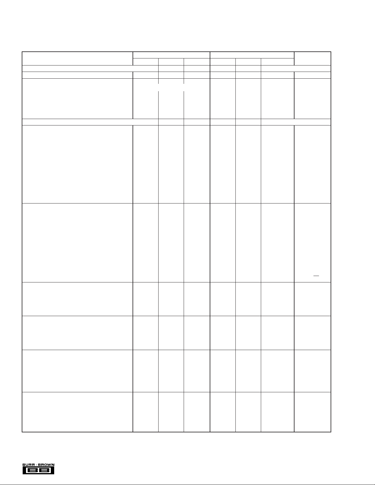
DESCRIPTION
DAC712 is a complete 16-bit resolution D/A converter
with 16 bits of monotonicity over temperature.
DAC712 has a precision +10V temperature compensated voltage reference, ±10V output amplifier and
16-bit port bus interface.
The digital interface is fast, 60ns minimum write pulse
width, is double-buffered and has a CLEAR function
that resets the analog output to bipolar zero.
GAIN and OFFSET adjustment inputs are arranged so
that they can be easily trimmed by external D/A
converters as well as by potentiometers.
DAC712 is available in two linearity error performance grades: ±4LSB and ±2LSB and three differential linearity grades: ±4LSB, ±2LSB, and ±1LSB. The
DAC712 is specified at power supply voltages of
±12V and ±15V.
DAC712 is packaged in a 28-pin 0.3" wide plastic DIP
and in a 28-lead wide-body plastic SOIC. The
DAC712P, U, PB, UB, are specified over the –40°C to
+85°C temperature range and the DAC712PK, UK,
PL, UL are specified over the 0°C to +70°C range.
DB
15
A
1
A
0
WR
CLR
Reference
Circuit
Gain Adjust
International Airport Industrial Park • Mailing Address: PO Box 11400, Tucson, AZ 85734 • Street Address: 6730 S. Tucson Blvd., Tucson, AZ 85706 • Tel: (520) 746-1111 • Twx: 910-952-1111
Internet: http://www.burr-brown.com/ • FAXLine: (800) 548-6133 (US/Canada Only) • Cable: BBRCORP • Telex: 066-6491 • FAX: (520) 889-1510 • Immediate Product Info: (800) 548-6132
© 1994 Burr-Brown Corporation PDS-1164G Printed in U.S.A. May, 1998
V
REF OUT
+10V
Input Latch
16
D/A Latch
16
16-Bit D/A Converter
Bipolar Offset Adjust
V
OUT
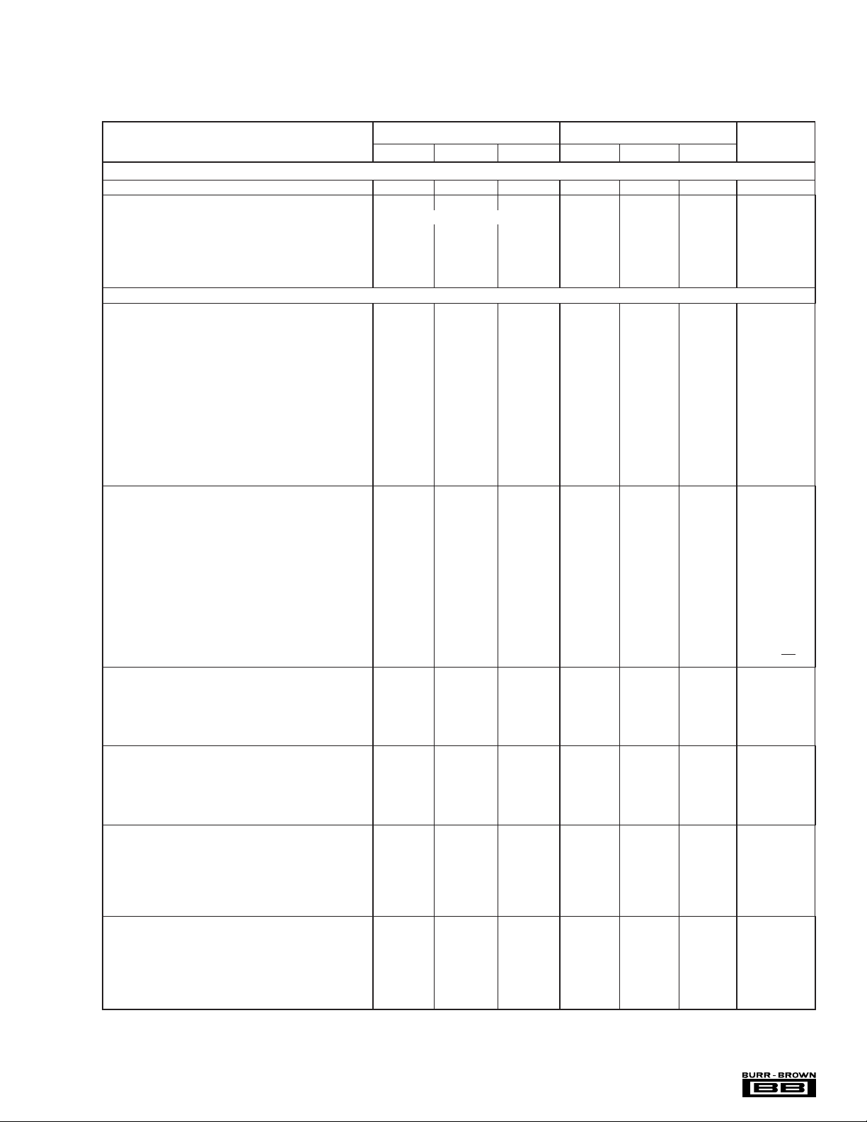
SPECIFICATIONS
ELECTRICAL
At TA = 25°C, +V
PARAMETER MIN TYP MAX MIN TYP MAX UNITS
INPUT
RESOLUTION 16 ✻ Bits
DIGITAL INPUTS
Input Code Binary Two’s Complement ✻
Logic Levels
V
IH
V
IL
(VI = +2.7V) ±10 ✻ µA
I
IH
(V
I
IL
I
TRANSFER CHARACTERISTICS
ACCURACY
Linearity Error ±4 ±2 LSB
to T
T
MIN
Differential Linearity Error ±4 ±2 LSB
to T
T
MIN
Monotonicity Over Temp 13 14 Bits
Gain Error
to T
T
MIN
Bipolar Zero Error
to T
T
MIN
Power Supply Sensitivity Of Full Scale: ±0.003 ✻ % FSR/% V
DYNAMIC PERFORMANCE
Settling Time (to ±0.003%FSR, 5kΩ || 500pF Load)
20V Output Step 6 ✻ 10 µs
1 LSB Output Step
Output Slew Rate 10 ✻ V/µs
Total Harmonic Distortion + Noise
0dB, 1001Hz, f
–20dB, 1001Hz, f
–60dB, 1001Hz, f
SINAD
1001Hz, f
Digital Feedthrough
Digital-to-Analog Glitch Impulse
Output Noise Voltage (Includes Reference) 120 ✻ nV/√Hz
ANALOG OUTPUT
Output Voltage Range
, –VCC = ±11.4V ±10 ✻ V
+V
CC
Output Current ±5 ✻ mA
Output Impedance 0.1 ✻ Ω
Short Circuit to ACOM, Duration Indefinite ✻
REFERENCE VOLTAGE
Voltage +9.975 +10.000 +10.025 ✻✻ ✻ V
to T
T
MIN
Output Resistance 1 ✻ Ω
Source Current 2 ✻ mA
Short Circuit to ACOM, Duration Indefinite ✻
POWER SUPPLY REQUIREMENTS
Voltage: +V
Current (No Load, ±15V Supplies)
Power Dissipation
TEMPERATURE RANGES
Specification
All Grades –40 +85 ✻✻°C
Storage –60 +150 ✻✻°C
Thermal Coefficient
DIP Package 75 ✻ °C/W
SOIC Package 75 ✻ °C/W
✻ Specifications are the same as grade to the left.
NOTES: (1) Digital inputs are TTL and +5V CMOS compatible over the specification temperature range. (2) FSR means Full Scale Range. For example, for a ±10V
output, FSR = 20V. (3) Errors externally adjustable to zero. (4) Maximum represents the 3σ limit. Not 100% tested for this parameter. (5) For the worst case code changes:
to 0000
FFFF
HEX
= +12V and +15V, –V
CC
= –12V and –15V, unless otherwise noted.
CC
DAC712P, U DAC712PB, UB
(1)
+2.0
0 +0.8 ✻✻V
+V
CC
– 1.4
✻✻V
= +0.4V) ±10 ✻ µA
MAX
MAX
(3)
MAX
(3)
±8 ±4 LSB
±8 ±4 LSB
±0.1 ±0.1 %
±0.2 ±0.15 %
±0.1 ✻ % FSR
±20 ✻ mV
MAX
±0.2 ±0.15 % FSR
±40 ±30 mV
±30 ✻ ppm FSR/% V
(4)
(5)
= 100kHz 0.005 ✻ %
S
= 100kHz 0.03 ✻ %
S
= 100kHz 3.0 ✻ %
S
= 100kHz 87 ✻ dB
S
–V
+V
–V
MAX
CC
CC
CC
CC
(6)
and 0000
HEX
®
(5)
θ
JA
HEX
(5)
to FFFF
+9.960 +10.040 ✻✻V
+11.4 +15 +16.5 ✻✻ ✻ V
–11.4 –15 –16.5 ✻✻ ✻ V
. These are Binary Two’s Complement (BTC) codes. (6) Typical supply voltages times maximum currents.
HEX
DAC712
4 ✻ µs
2 ✻ nV-s
15 ✻ nV-s
13 15 ✻✻ mA
22 25 ✻✻ mA
525 600 ✻✻ mW
2
(2)
CC
CC
SPECIFICATIONS
ELECTRICAL
At TA = +25°C, +V
PARAMETER MIN TYP MAX MIN TYP MAX UNITS
INPUT
RESOLUTION 16 ✻ Bits
DIGITAL INPUTS
Input Code Binary Two’s Complement ✻
Logic Levels
V
IH
V
IL
(VI = +2.7V) ±10 ✻ µA
I
IH
(VI = +0.4V) ±10 ✻ µA
I
IL
TRANSFER CHARACTERISTICS
ACCURACY
Linearity Error ±2 ±2 LSB
to T
T
MIN
Differential Linearity Error ±2 ±1 LSB
to T
T
MIN
Monotonicity Over Temp 15 16 Bits
Gain Error
to T
T
MIN
Bipolar Zero Error
to T
T
MIN
Power Supply Sensitivity of Full Scale ±0.003 ✻ %FSR/% V
DYNAMIC PERFORMANCE
Settling Time (to ±0.003%FSR, 5kΩ || 500pF Load)
20V Output Step 6 10 ✻ 10 µs
1LSB Output Step
Output Slew Rate 10 ✻ V/µs
Total Harmonic Distortion + Noise
0dB, 1001Hz, f
–20dB, 1001Hz, f
–60dB, 1001Hz, f
SINAD
1001Hz, f
Digital Feedthrough
Digital-to-Analog Glitch Impulse
Output Noise Voltage (includes reference) 120 ✻ nV/√Hz
ANALOG OUTPUT
Output Voltage Range
, –VCC = ±11.4V ±10 ✻ V
+V
CC
Output Current ±5 ✻ mA
Output Impedance 0.1 ✻ Ω
Short Circuit to ACOM, Duration Indefinite ✻
REFERENCE VOLTAGE
Voltage +9.975 +10.000 +10.025 ✻✻✻ V
to T
T
MIN
Output Resistance 1 ✻ Ω
Source Current 2 ✻ mA
Short Circuit to ACOM, Duration Indefinite ✻
POWER SUPPLY REQUIREMENTS
Voltage: +V
Current (No Load, ±15V Supplies)
Power Dissipation
TEMPERATURE RANGES
Specification
All Grades 0 +70 ✻✻°C
Storage –60 +150 ✻✻°C
Thermal Coefficient,
DIP Package 75 ✻ °C/W
SOIC Package 75 ✻ °C/W
✻ Same specification as grade to the left.
NOTES: (1) Digital inputs are TTL and +5V CMOS compatible over the specification temperature range. (2) FSR means Full Scale Range. For example, for a ±10V
output, FSR = 20V. (3) Errors externally adjustable to zero. (4) Maximum represents the 3σ limit. Not 100% tested for this parameter. (5) For the worst case code changes:
FFFF
to 0000
HEX
= +12V and +15V, –VCC = –12V and –15V, unless otherwise noted.
CC
DAC712PK, UK DAC712PL, UL
(1)
+2.0 +VCC – 1.4 ✻✻V
0 +0.8 ✻✻V
MAX
MAX
(3)
MAX
(3)
±2 ±2 LSB
±2 ±1 LSB
±0.1 ✻ %
±0.15 ±0.02 %
±0.1 ✻ % FSR
±20 ✻ mV
MAX
±0.15 ±0.15 % FSR
±30 ✻ mV
±30 ✻ ppm FSR/% V
(4)
(5)
= 100kHz 0.005 ✻ %
S
= 100kHz 0.03 ✻ %
S
= 100kHz 3.0 ✻ %
S
= 100kHz 87 ✻ dB
S
+V
–V
–V
MAX
CC
CC
CC
CC
(6)
and 0000
HEX
(5)
θ
(5)
+9.960 +10.040 ✻✻V
+11.4 +15 +16.5 ✻✻✻ V
–11.4 –15 –16.5 ✻✻✻ V
JA
HEX
to FFFF
. These are Binary Two’s Complement (BTC) codes. (6) Typical supply voltages times maximum currents.
HEX
4 ✻ µs
2 ✻ nV–s
15 ✻ nV–s
13 15 ✻✻ mA
22 25 ✻✻ mA
525 600 ✻ mW
3
DAC712
(2)
CC
CC
®
ABSOLUTE MAXIMUM RATINGS
+VCC to COMMON ...................................................................... 0V, +17V
–V
to COMMON ...................................................................... 0V, –17V
CC
to –VCC........................................................................................ 34V
+V
CC
Digital Inputs to COMMON .......................................... –1V to +V
External Voltage Applied to BPO and Range Resistors..................... ±V
V
V
Power Dissipation .......................................................................... 750mW
Storage Temperature ...................................................... –60°C to +150°C
Lead Temperature (soldering, 10s)................................................ +300°C
NOTE: Stresses above those listed under “Absolute Maximum Ratings” may
cause permanent damage to the device. Exposure to absolute maximum
conditions for extended periods may affect device reliability.
...................................................... Indefinite Short to COMMON
REF OUT
............................................................ Indefinite Short to COMMON
OUT
CC
–0.7V
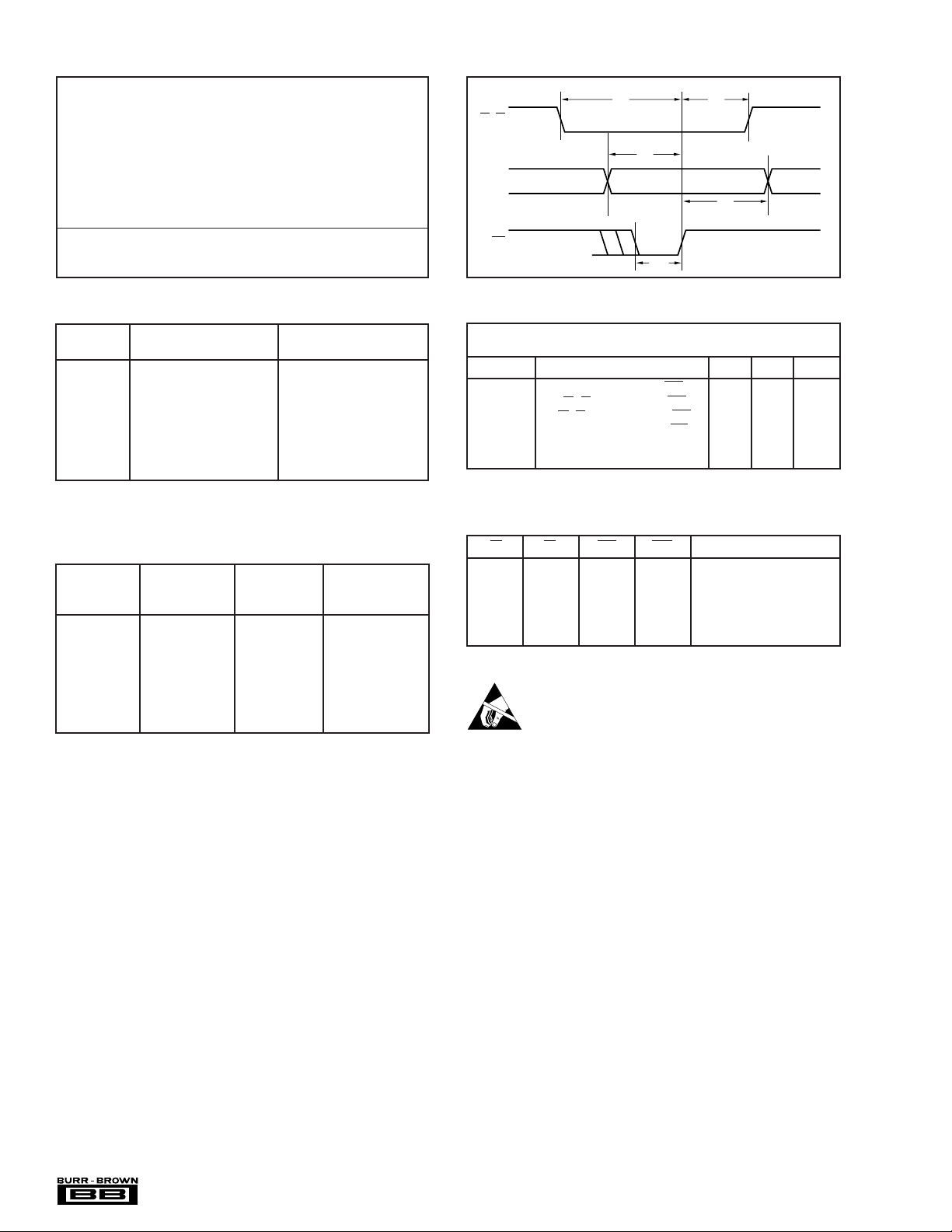
TIMING DIAGRAM
t
AW
A
, A
0
1
CC
D0-D15
WR
t
DW
t
WP
t
AH
t
DH
PACKAGE INFORMATION
PRODUCT PACKAGE NUMBER
PACKAGE DRAWING
DAC712P Plastic DIP 246
DAC712U Plastic SOIC 217
DAC712PB Plastic DIP 246
DAC712UB Plastic SOIC 217
DAC712PK Plastic DIP 246
DAC712UK Plastic SOIC 217
DAC712PL Plastic DIP 246
DAC712UL Plastic SOIC 217
NOTE: (1) For detailed drawing and dimension table, please see end of data
sheet, or Appendix C of Burr-Brown IC Data Book.
(1)
ORDERING INFORMATION
PRODUCT RANGE at +25
TEMPERATURE ERROR MAX LINEARITY ERROR
DAC712P –40°C to +85°C ±4LSB ±4LSB
DAC712U –40°C to +85°C ±4LSB ±4LSB
DAC712PB –40°C to +85°C ±2LSB ±2LSB
DAC712UB –40°C to +85°C ±2LSB ±2LSB
DAC712PK 0°C to +70°C ±2LSB ±2LSB
DAC712UK 0°C to +70°C ±2LSB ±2LSB
DAC712PL 0°C to +70°C ±2LSB ±1LSB
DAC712UL 0°C to +70°C ±2LSB ±1LSB
LINEARITY DIFFERENTIAL
°C MAX at +25°C
TIMING SPECIFICATIONS
TA = –40°C to +85°C, +VCC = +12V or +15V, –VCC = –12V or –15V.
SYMBOL PARAMETER MIN MAX UNITS
t
DW
t
AW
t
AH
t
DH
(1)
t
WP
t
CP
NOTES: (1) For single-buffered operation, t
Data Valid to End of WR 50 ns
A0, A1 Valid to End of WR 50 ns
A0, A1 Hold after End of WR 10 ns
Data Hold after end of WR 10 ns
Write Pulse Width 50 ns
CLEAR Pulse Width 200 ns
is 80ns min. Refer to page 10.
WP
TRUTH TABLE
A
011 → 0 → 1 1 Load Input Latch
101 → 0 → 1 1 Load D/A Latch
111 → 0 → 1 1 No Change
0 0 0 1 Latches Transparent
X X 1 1 No Change
X X X 0 Reset D/A Latch
A
0
1
WR CLR DESCRIPTION
ELECTROSTATIC
DISCHARGE SENSITIVITY
Electrostatic discharge can cause damage ranging from performance degradation to complete device failure. Burr-Brown
Corporation recommends that all integrated circuits be handled
and stored using appropriate ESD protection methods.
ESD damage can range from subtle performance degradation
to complete device failure. Precision integrated circuits may
be more susceptible to damage because very small parametric
changes could cause the device not to meet published specifications.
®
DAC712
4
 Loading...