

Burr Brown Corporation DAC709, DAC707KP-BI, DAC707KP, DAC707JP-BI, DAC707 Datasheet
Microprocessor-Compatible
16-BIT DIGITAL-TO-ANALOG CONVERTERS
FEATURES
● TWO-CHIP CONSTRUCTION
● HIGH-SPEED 16-BIT PARALLEL, 8-BIT
(BYTE) PARALLEL, AND SERIAL INPUT
MODES
● DOUBLE-BUFFERED INPUT REGISTER
CONFIGURATION
● V
OUT
AND I
OUT
MODELS
● HIGH ACCURACY:
Linearity Error
±0.003% of FSR max
Differential Linearity Error
±0.006% of FSR
max
● MONOTONIC (TO 14 BITS) OVER
SPECIFIED TEMPERATURE RANGE
● HERMETICALLY SEALED
● LOW COST PLASTIC VERSIONS
AVAILABLE (DAC707JP/KP)
DESCRIPTION
The DAC708 and DAC709 are 16-bit converters designed to interface to an 8-bit microprocessor bus. 16bit data is loaded in two successive 8-bit bytes into
parallel 8-bit latches before being transferred into the
D/A latch. The DAC708 and DAC709 are current and
voltage output models respectively and are in 24-pin
hermetic DIPs. Input coding is Binary Two’s Complement (bipolar) or Unipolar Straight Binary (unipolar,
when an external logic inverter is used to invert the
MSB). In addition, the DAC708/709 can be loaded
serially (MSB first).
The DAC707 is designed to interface to a 16-bit bus.
Data is written into a 16-bit latch and subsequently the
D/A latch. The DAC707 has bipolar voltage output
and input coding is Binary Two’s Complement (BTC).
All models have Write and Clear control lines as well
as input latch enable lines. In addition, DAC708 and
DAC709 have Chip Select control lines. In the bipolar
mode, the Clear input sets the D/A latch to give zero
voltage or current output. They are all 14-bit accurate
and are complete with reference, and for the DAC707,
and DAC709, a voltage output amplifier. All models
are available with an optional burn-in screening.
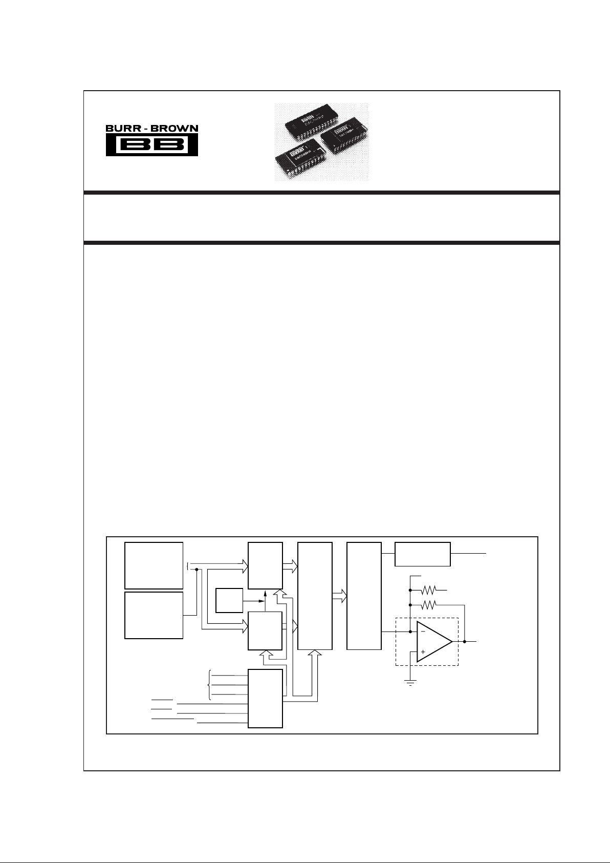
DAC707/708/709 Block Diagram
High
Byte
Latch
Latch Enables/
Mode Select
Control
Logic
CLEAR
WRITE
CHIP SELECT
16-Bit
D/A
Con-
verter
DAC707 or DAC709
Only
Summing Junction (708, 709)
10V Range (708, 709)
V
OUT
Reference
Circuit
Bipolar
Offset
Low
Byte
Latch
D/A
Latch
Serial
(DAC708, 709)
8-Bit
(DAC708, 709)
or
16-Bit (DAC707)
Serial
Data
PDS-557H
®
International Airport Industrial Park • Mailing Address: PO Box 11400, Tucson, AZ 85734 • Street Address: 6730 S. Tucson Blvd., Tucson, AZ 85706 • Tel: (520) 746-1111 • Twx: 910-952-1111
Internet: http://www.burr-brown.com/ • FAXLine: (800) 548-6133 (US/Canada Only) • Cable: BBRCORP • Telex: 066-6491 • FAX: (520) 889-1510 • Immediate Product Info: (800) 548-6132
DAC707
DAC708
DAC709
®
DAC707/708/709
2
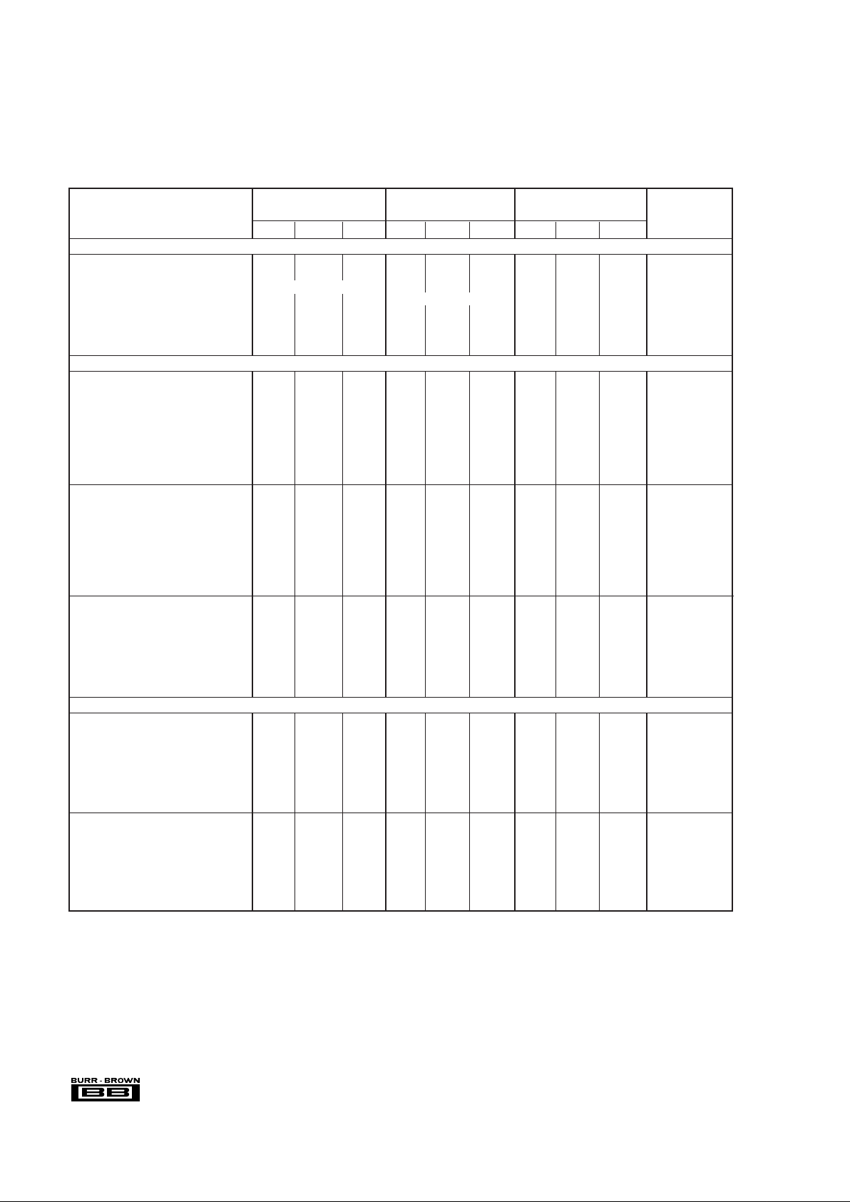
SPECIFICATIONS
ELECTRICAL
At TA = +25°C, V
CC
= ±15V, V
DD
= +5V, and after a 10-minute warm-up, unless otherwise noted.
DAC707/708/709KH, DAC707/708/
DAC707JP DAC707KP 709BH, SH
PRODUCT MIN TYP MAX MIN TYP MAX MIN TYP MAX UNITS
INPUT
DIGITAL INPUT
Resolution 16 * * Bits
Bipolar Input Code (all models) Binary Two’s Complement * *
Unipolar Input Code
(1)
(DAC708/709 only) Unipolar Straight Binary *
Logic Levels
(2)
: V
IH
+2.0 +5.5 * * * * V
V
IL
–1.0 +0.8 * * * * V
I
IH
(VI = +2.7V) 1 * * µA
I
IL
(VI = +0.4V) 1 * * µA
TRANSFER CHARACTERISTICS
ACCURACY
(3)
Linearity Error ±0.003 ±0.006 ±0.0015 ±0.003 * * % of FSR
(4)
Differential Linearity Error
(5)
±0.0045 ±0.012 ±0.003 ±0.006 * * % of FSR
at Bipolar Zero
(5, 6)
±0.003 ±0.006 ±0.0015 ±0.003 % of FSR
Gain Error
(7)
±0.07 ±0.30 * ±0.15 ±0.05 ±0.10 %
Zero Error
(7)
±0.05 ±0.1 * * * * % of FSR
Monotonicity Over Spec Temp Range 13 14 14 Bits
Power Supply Sensitivity: +V
CC,
–V
CC
±0.0015 ±0.006 * * * ±0.003 % of FSR/%V
CC
V
DD
±0.0001 ±0.001 * * * * % of FSR/%V
DD
DRIFT (Over Spec Temp Range
(3)
)
Total Error Over Temp Range
(8)
±0.08 * ±0.15 * ±0.10 % of FSR
Total Full Scale Drift ±10 * ±25 * ±15 ppm of FSR/°C
Gain Drift ±10 ±30 * ±25 ±7 ±15 ppm/°C
Zero Drift: Unipolar (DAC708/709 only) ±2.5 ±5 ±1.5 ±3 ppm of FSR/°C
Bipolar (all models) ±5 ±15 * ±12 ±4 ±10 ppm of FSR/°C
Differential Linearity Over Temp
(5)
±0.012 +0.009, *
–0.006 % of FSR
Linearity Error Over Temp
(5)
±0.012 ±0.006 * % of FSR
SETTLING TIME (to ±0.003% of FSR)
(9)
Voltage Output Models
Full Scale Step (2kΩ load) 4 * 8 * 8 µs
1LSB Step at Worst Case Code
(10)
2.5 * 4 * 4 µs
Slew Rate 10 * * V/µs
Current Output Models
Full Scale Step (2mA): 10 to 100Ω Load 350 * ns
1kΩ Load 1 * µs
OUTPUT
VOLTAGE OUTPUT MODELS
Output Voltage Range
DAC709: Unipolar (USB Code) 0 to +10 * V
Bipolar (BTC Code) ±5, ±10 * V
DAC707 Bipolar (BTC Code) ±10 * * V
Output Current ±5** mA
Output Impedance 0.15 * * Ω
Short Circuit to Common Duration Indefinite * *
CURRENT OUTPUT MODELS
Output Current Range (±30% typ)
DAC708: Unipolar (USB Code) 0 to –2 * mA
Bipolar (BTC Code) ±1*mA
Unipolar Output Impedance (±30% typ) 4.0 * kΩ
Bipolar Output Impedance (±30% typ) 2.45 * kΩ
Compliance Voltage ±2.5 * V
The information provided herein is believed to be reliable; however, BURR-BROWN assumes no responsibility for inaccuracies or omissions. BURR-BROWN assumes
no responsibility for the use of this information, and all use of such information shall be entirely at the user’s own risk. Prices and specifications are subject to change
without notice. No patent rights or licenses to any of the circuits described herein are implied or granted to any third party. BURR-BROWN does not authorize or warrant
any BURR-BROWN product for use in life support devices and/or systems.
3
®
DAC707/708/709
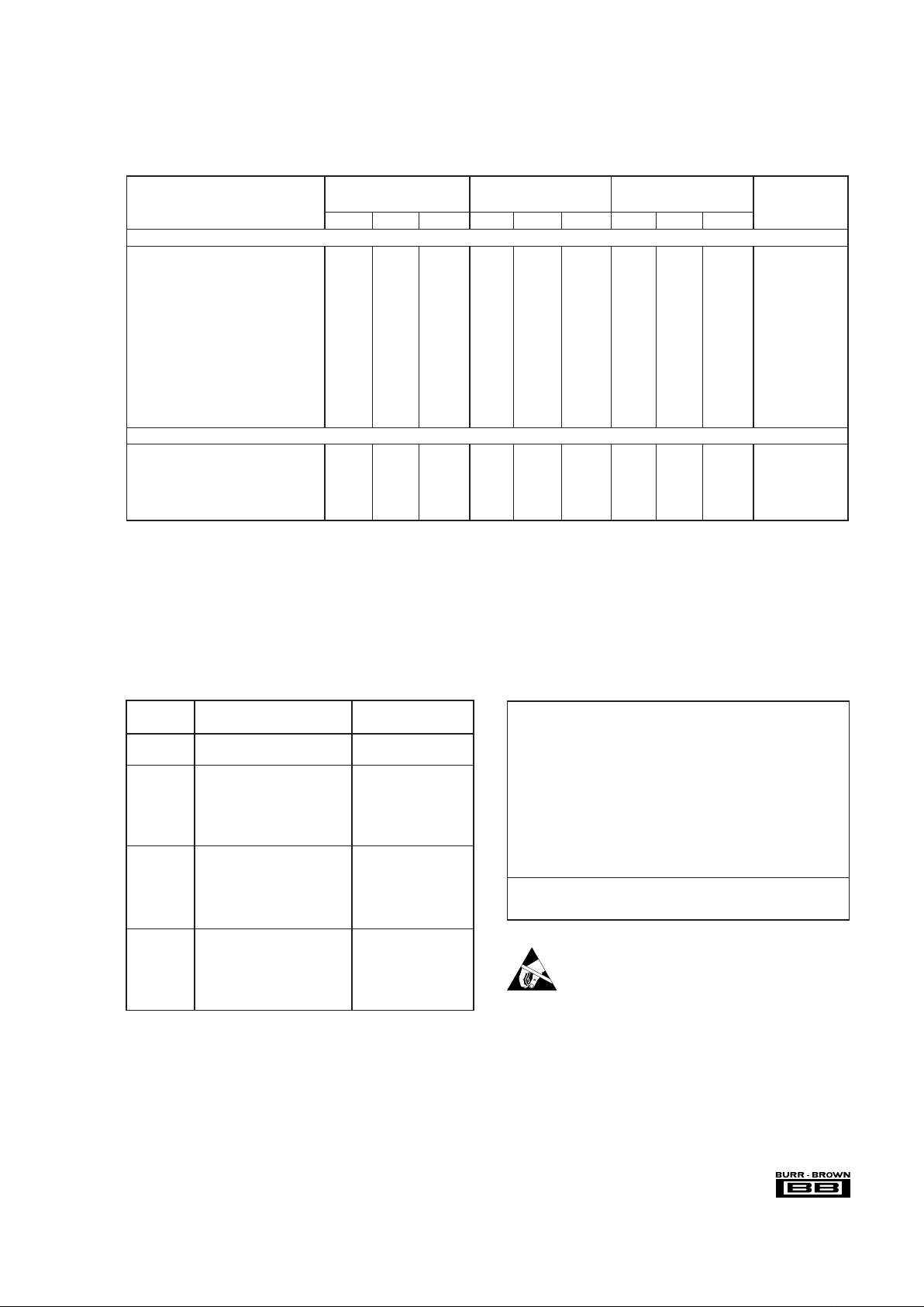
PACKAGE DRAWING
PRODUCT PACKAGE NUMBER
(1)
DAC707JP 28-Pin Plastic DBL Wide DIP 215
DAC707KP 28-Pin Plastic DBL Wide DIP 215
DAC707BH 28LD Side Brazed 149
Hermetic Dip
DAC707KH 28LD Side Brazed 149
Hermetic DIP
DAC707SH 28LD Side Brazed 149
Hermetic DIP
DAC708BH 24LD Side Brazed 165
Hermetic DIP
DAC708KH 24LD Side Brazed 165
Hermetic DIP
DAC708SH 24LD Side Brazed 165
Hermetic DIP
DAC709BH 24LD Side Brazed 165
Hermetic DIP
DAC709KH 24LD Side Brazed 165
Hermetic DIP
DAC709SH 24LD Side Brazed 165
Hermetic DIP
NOTE: (1) For detailed drawing and dimension table, please see end of data
sheet, or Appendix C of Burr-Brown IC Data Book.
DAC707/708/709KH, DAC707/708/
DAC707JP DAC707KP 709BH, SH
PRODUCT MIN TYP MAX MIN TYP MAX MIN TYP MAX UNITS
At T
A
= +25°C, V
CC
= ±15V, V
DD
= +5V, and after a 10-minute warm-up, unless otherwise noted.
ELECTRICAL (CONT)
*Specification same as for models in column to the left.
NOTES: (1) MSB must be inverted externally prior to DAC708/709 input. (2) Digital inputs are TTL, LSTTL, 54/74C, 54/74HC and 54/74HTC compatible over the specified
temperature range. (3) DAC708 (current-output models) are specified and tested with an external output operational amplifier connected using the internal feedback
resistor in all tests. (4) FSR means Full Scale Range. For example, for ±10V output, FSR = 20V. (5) ±0.0015% of Full Scale Range is equal to 1 LSB in 16-bit resolution,
±0.003% of Full Scale Range is equal to 1 LSB in 15-bit resolution. ±0.006% of Full Scale Range is equal to 1 LSB in 14-bit resolution. (6) Error at input code 0000
H
.
(For unipolar connection on DAC708/709, the MSB must be inverted externally prior to D/A input.) (7) Adjustable to zero with external trim potentiometer. Adjusting the
gain potentiometer rotates the transfer function around the bipolar zero point. (8) With gain and zero errors adjusted to zero at +25°C. (9) Maximum represents the 3σ
limit. Not 100% tested for this parameter. (10) The bipolar worst-case code change is FFFF
H
to 0000H and 0000H to FFFFH. For unipolar (DAC708/709 only) it is 7FFF
H
to 8000H and 8000H to 7FFFH.
POWER SUPPLY REQUIREMENTS
Voltage (all models): +V
CC
+13.5 +15 +16.5 * * * * * * V
–V
CC
–13.5 –15 –16.5 * * * * * * V
V
DD
+4.5 +5 +5.5 * * * * * * V
Current (No Load, +15V Supplies)
Current Output Models: +V
CC
+10 +25 * * mA
–V
CC
–13 –25 * * mA
V
DD
+5 +10 * * mA
Voltage Output Models: +V
CC
+16 +30 * * * * mA
–V
CC
–18 –30 * * * * mA
V
DD
+5 +10 * * * * mA
Power Dissipation (±15V supplies)
Current Output Models 370 800 * * mW
Voltage Output Models 535 * 950 * * mW
TEMPERATURE RANGE
Specification: BH Grades –25 +85 °C
JP, KP, KH Grades 0 +70 * * °C
SH Grades –55 +125 °C
Storage: Ceramic –65 +150 –65 +150 °C
Plastic –60 +100 * * °C
PACKAGE INFORMATION
ABSOLUTE MAXIMUM RATINGS
VDD to COMMON ........................................................................ 0V, +15V
+V
CC
to COMMON ..................................................................... 0V, +18V
–V
CC
to COMMON ...................................................................... 0V, –18V
Digital Data Inputs to COMMON ..................................... –0.5V, V
DD
+0.5
DC Current any input ..................................................................... ±10mA
Reference Out to COMMON ...................... Indefinite Short to COMMON
V
OUT
(DAC707, DAC709) ........................... Indefinite Short to COMMON
External Voltage Applied to R
F
(pin 13 or 14, DAC708) .................. ±18V
External Voltage Applied to D/A Output
(pin 1, DAC707; pin 14, DAC709) ......................................................... ±5V
Power Dissipation ........................................................................ 1000mW
Storage Temperature ..................................................... –60°C to +150 °C
Lead Temperature (soldering, 10s)................................................. 300°C
Stresses above those listed under “Absolute Maximum Ratings” may
cause permanent damage to the device. Exposure to absolute maximum
conditions for extended periods may affect device reliability.
ELECTROSTATIC
DISCHARGE SENSITIVITY
This integrated circuit can be damaged by ESD. Burr-Brown
recommends that all integrated circuits be handled with
appropriate precautions. Failure to observe proper handling
and installation procedures can cause damage.
ESD damage can range from subtle performance degradation
to complete device failure. Precision integrated circuits may
be more susceptible to damage because very small parametric
changes could cause the device not to meet its published
specifications.
®
DAC707/708/709
4
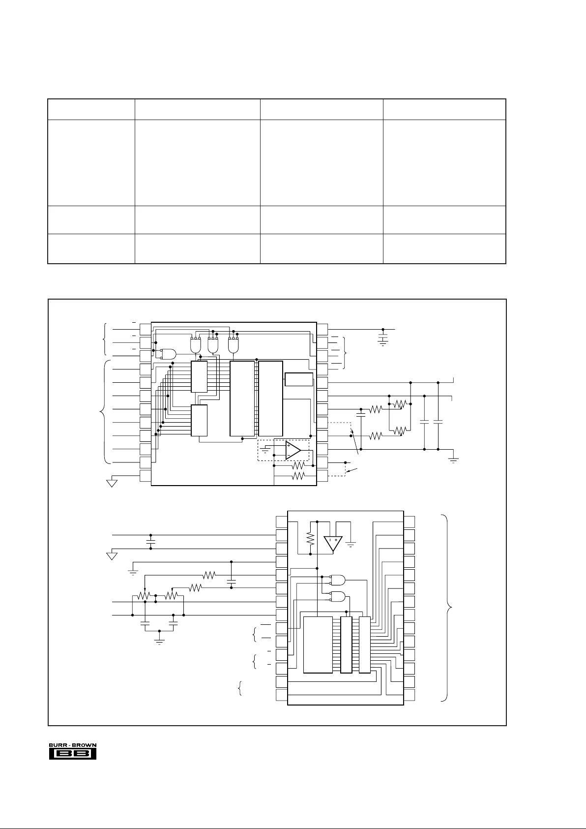
CONNECTION DIAGRAMS
F2
OUT
A
A
A
D7 (D15)
D6 (D14)
D5 (D13)
D4 (D12)
D3 (D11)
D2 (D10)
D1 (D9)
D0 (D8)/S1
DCOM
24
23
22
21
20
19
18
17
16
15
14
13
28
27
26
25
24
23
22
21
20
19
18
17
16
15
1
2
3
4
5
6
7
8
9
10
11
12
1
2
3
4
5
6
7
8
9
10
11
12
13
14
V
CS
WR
CLR
–V
+V
GA
BPO
SJ
ACOM
V
R
DD
CC
F
CC
DD
V
+
(2)
(2)
(2)
(3)
+
+
CC
CC
–V
+V
(1)
(1)
3.9M
270k
Offset Adjust
Gain
Adjust
Ω
Ω
Control
Lines
Connect for bipolar operation.
Connect for 10V range.
Leave pin 13 open for 20V range.
+
ΩΩ
10kΩ
DAC709
Only
16-Bit
Ladder
Resistor
Network
and
Current
Switches
Reference
Circuit
D/A
Latch
Low
Byte
Latch
High
Byte
Latch
2
0
1
D0 (LSB)
D1
D2
D3
D4
D5
D6
D7
D8
D9
D10
D11
D12
D13
R
16-Bit
Ladder
Resistor
Network
and
Current
Switches
D/A Latch
Input Latch
Digital
Inputs
V
+V
–V
V
CLR
WR
A
A
0
1
(2)
(3)
(1)
3.9M
270kΩΩ
NOTES: (1) Potentiometers are 10k to 100k .
(2) Decoupling capcitors are 0.1µF to 1.0µF.
(3) By
pass, 0.0022µF to 0.01µF.
DD
CC
–V
CC
+V
(2)
Digital Inputs
Latch Enable Lines
Control Lines
Gain Adjust
Analog Common
CC
Offset
Adjust
Digital
Common
(2)
V
DD
OUT
NOTES: (1) Potentiometer is
10k to 100k . (2) Decoupling
capcitors are 0.1µF to 1.0µF.
DAC708/709
DAC707
Register
Enable
Lines
Data
Inputs
DCOM
ACOM
SJ
GA
(MSB) D15
D14
ΩΩ
10kΩ
CC
ORDERING INFORMATION
TEMPERATURE INPUT OUTPUT
PRODUCT RANGE CONFIGURATION CONFIGURATION
DAC707JP 0°C to +70°C 16-bit port ±10V output
DAC707JP-BI
(1)
0°C to +70°C 16-bit port ±10V output
DAC707KP 0°C to +70°C 16-bit port ±10V output
DAC707KP-BI
(1)
0°C to +70°C 16-bit port ±10V output
DAC707KH 0°C to +70°C 16-bit port ±10V output
DAC707KH-BI
(1)
0°C to +70°C 16-bit port ±10V output
DAC707BH –25°C to +85°C 16-bit port ±10V output
DAC707BH-BI
(1)
–25°C to +85°C 16-bit port ±10V output
DAC707SH –55°C to +125°C 16-bit port ±10V output
DAC707SH-BI
(1)
–55°C to +125°C 16-bit port ±10V output
DAC708KH 0°C to +70°C 8-bit port ±1mA output
DAC708BH –25°C to +85°C 8-bit port ±1mA output
DAC708SH –55°C to +125°C 8-bit port ±1mA output
DAC709KH 0°C to +70°C 8-bit port ±10V output
DAC709BH –25°C to +85°C 8-bit port ±10V output
DAC709SH –55°C to +125°C 8-bit port ±10V output
NOTE: (1) 25 piece minimum order.
 Loading...