


Burr Brown Corporation DAC1600KP-V, DAC1600JP-V, DAC703SH, DAC703LH, DAC703KP Datasheet
...
1
®
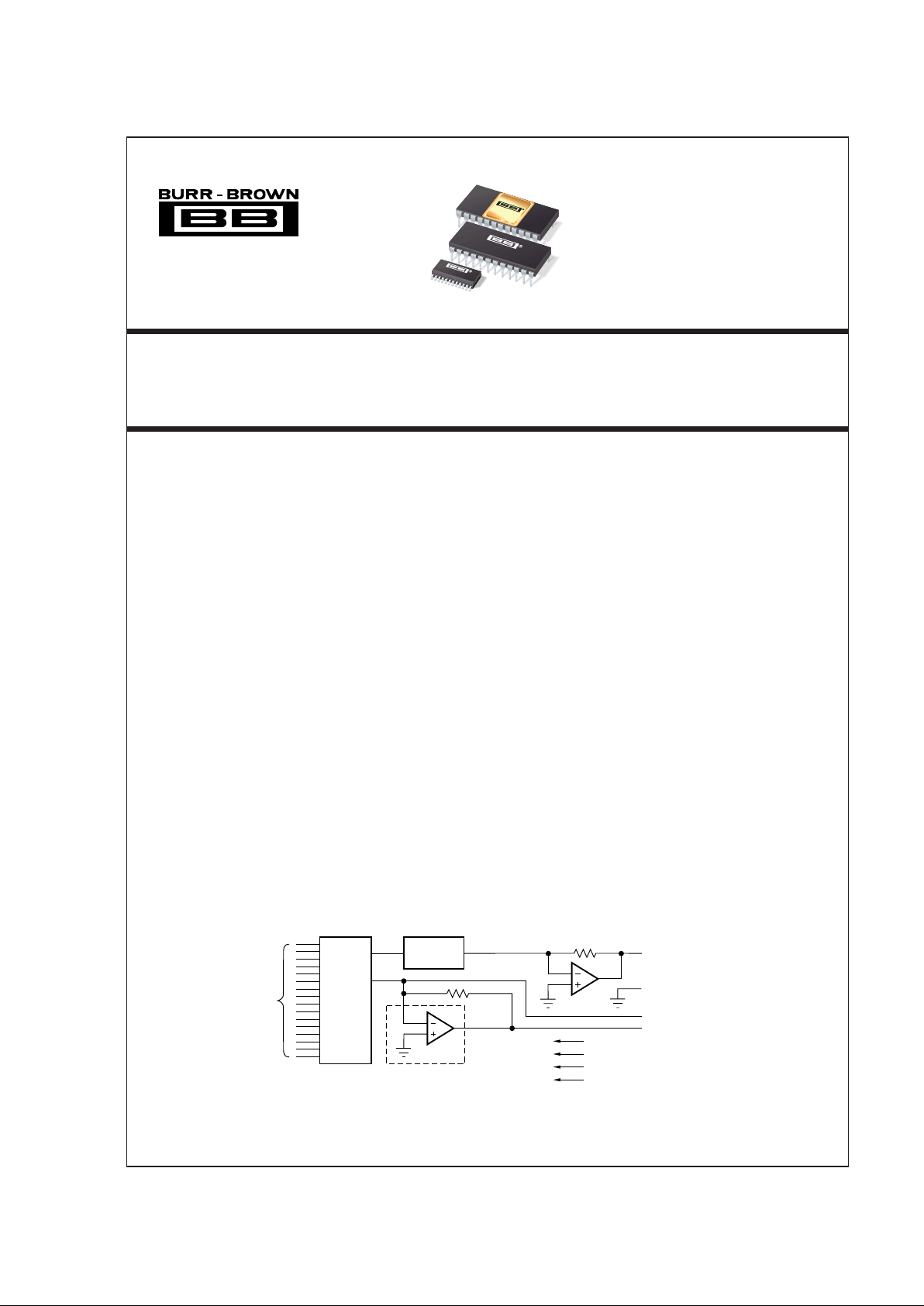
DAC701, 702, 703
Monolithic 16-Bit
DIGITAL-TO-ANALOG CONVERTERS
FEATURES
● V
OUT
AND I
OUT
MODELS
● HIGH ACCURACY:
Linearity Error
±0.0015% of FSR max
Differential Linearity Error
±0.003% of FSR
max
DAC701
DAC702
DAC703
®
16-Bit
Ladder
Resistor
Network
And
Current
Switches
Digital
Inputs
Reference
Circuit
Reference Output
Summing Junction
Output
Common
Gain Adjust
+V
–V
V
CC
CC
DD
Voltage Models
Only
International Airport Industrial Park • Mailing Address: PO Box 11400, Tucson, AZ 85734 • Street Address: 6730 S. Tucson Blvd., Tucson, AZ 85706 • Tel: (520) 746-1111 • Twx: 910-952-1111
Internet: http://www.burr-brown.com/ • FAXLine: (800) 548-6133 (US/Canada Only) • Cable: BBRCORP • Telex: 066-6491 • FAX: (520) 889-1510 • Immediate Product Info: (800) 548-6132
● MONOTONIC (at 15 bits) OVER FULL
SPECIFICATION TEMPERATURE RANGE
● PIN-COMPATIBLE WITH DAC70, DAC71,
DAC72
● DUAL-IN-LINE PLASTIC AND HERMETIC
CERAMIC AND SOIC
DESCRIPTION
The DAC70X family comprise of complete 16-bit
digital-to-analog converters that includes a precision
buried-zener voltage reference and a low-noise, fastsettling output operational amplifier (voltage output
models), all on one small monolithic chip. A combination of current-switch design techniques accomplishes
not only 15-bit monotonicity over the entire specified
temperature range, but also a maximum end-point
linearity error of ±0.0015% of full-scale range. Total
full-scale gain drift is limited to ±10ppm/°C maximum
(LH and CH grades).
Digital inputs are complementary binary coded and
are TTL-, LSTTL-, 54/74C- and 54/74HC-compatible
over the entire temperature range. Outputs of 0 to
+10V, ±10V, 0 to –2mA, and ±1mA are available.
These D/A converters are packaged in hermetic 24-pin
ceramic side-brazed or molded plastic. The DIP-packaged parts are pin-compatible with the voltage and
current output DAC71 and DAC72 model families.
The DAC702 is also pin-compatible with the DAC70
model family. In addition, the DAC703 is offered in a
24-pin SOIC package for surface mount applications.
© 1983 Burr-Brown Corporation PDS-494M Printed in U.S.A. March, 1998
DAC701
DAC702
DAC703

2
®
DAC701, 702, 703
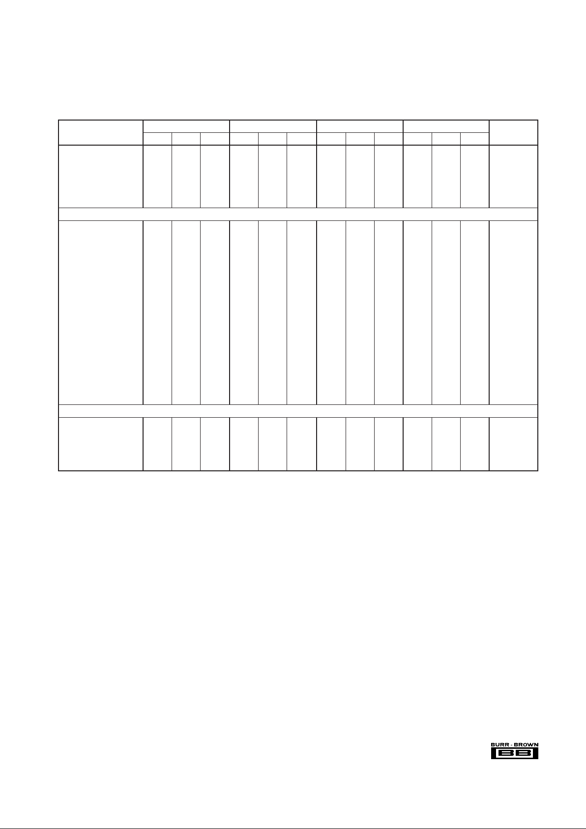
SPECIFICATIONS
At +25°C and rated power supplies, unless otherwise noted.
DAC702/703J DAC701/702/703K DAC701/702/703B, S DAC701/702/703L, C
PARAMETER MIN TYP MAX MIN TYP MAX MIN TYP MAX MIN TYP MAX UNITS
INPUT
DIGITAL INPUT
Resolution 16 ✻✻✻Bits
Digital Inputs
(1)
V
IH
+2.4 +V
CC
✻✻✻✻✻✻V
V
IL
–1.0 +0.8 ✻✻✻✻✻✻V
I
IH
, VI = +2.7V +40 ✻✻✻µA
I
IL
, VI = +0.4V –0.35 –0.5 ✻ ✻ ✻✻ ✻✻ mA
TRANSFER CHARACTERISTICS
ACCURACY
(2)
Linearity Error
(4)
±0.0015 ±0.006 ✻ ±0.003 ✻✻ ±0.00075 ±0.0015 % of FSR
(3)
Differential Linearity
Error
(4)
±0.003 ±0.012 ✻ ±0.006 ✻✻ ±0.0015 ±0.003 % of FSR
Differential Linearity
Error at Bipolar Zero
(DAC702/703)
(4)
±0.003 ±0.006 ±0.0015 ±0.003 ✻✻% of FSR
Gain Error
(5)
±0.07 ±0.30 ✻ ±0.15 ±0.05 ±0.10 ✻✻ %
Zero Error
(5, 6)
±0.05 ±0.10 ✻ ✻ ✻✻ ✻✻% of FSR
Monotonicity Over Spec.
Temp Range 13 14 ✻ 15 Bits
DRIFT (over specification
temperature range)
Total Error Over
Temperature Range
(all models)
(7)
±0.08 ✻ ±0.15 ±0.05 ±0.10 ✻✻% of FSR
Total Full Scale Drift:
DAC701 ±10 ✻ ±30 ±8.5 ±18 ±6 ±13 ppm of FSR/°C
DAC702/703 ±10 ✻ ±25 ±7 ±15 ✻✻ppm of FSR/°C
Gain Drift (all models) ±10 ±30 ✻ ±25 ±7 ±15 ±5 ±10 ppm/°C
Zero Drift:
DAC701 ±2.5 ±5 ±1.5 ±3 ✻✻ppm of FSR/°C
DAC702/703 ±5 ±15 ✻ ±12 ±4 ±10 ±2.5 ±5 ppm of FSR/°C
Differential Linearity
Over Temp.
(4)
±0.012 +0.009, ✻ +0.006, % of FSR
–0.006 –0.003
Linearity Error
Over Temp.
(4)
±0.012 ±0.006 ✻ ±0.003 % of FSR
SETTLING TIME (to
±0.003% of FSR)
(8)
DAC701/703 (V
OUT
Models)
Full Scale Step, 2kΩ Load 4 ✻ 8 ✻✻ ✻✻ µs
1LSB Step at
Worst-Case Code
(9)
2.5 ✻✻✻µs
Slew Rate 10 ✻✻✻V/µs
DAC702 (I
OUT
Models)
Full Scale Step (2mA),
10 to 100Ω Load 350 ✻ 1000 ✻✻ ✻✻ ns
1kΩ Load 1 ✻ 3 ✻✻ ✻✻ µs
OUTPUT
VOLTAGE OUTPUT
MODELS
DAC701 (CSB Code) 0 to +10 ✻ V
DAC703 (COB Code) ±10 ✻✻✻V
Output Current ±5 ✻✻✻ mA
Output Impedance 0.15 ✻✻✻Ω
Short Circuit to
Common Duration Indefinite ✻✻✻
CURRENT OUTPUT
MODELS
DAC702 (COB Code)
(10)
±1 ✻✻✻mA
Output Impedance
(10)
2.45 ✻✻✻kΩ
Compliance Voltage ±2.5 ✻✻✻V
3
®
DAC701, 702, 703
The information provided herein is believed to be reliable; however, BURR-BROWN assumes no responsibility for inaccuracies or omissions. BURR-BROWN assumes no
responsibility for the use of this information, and all use of such information shall be entirely at the user’s own risk. Prices and specifications are subject to change without notice.
No patent rights or licenses to any of the circuits described herein are implied or granted to any third party. BURR-BROWN does not authorize or warrant any BURR-BROWN
product for use in life support devices and/or systems.
DAC702/703J DAC701/702/703K DAC701/702/703B, S DAC701/702/703L, C
PARAMETER MIN TYP MAX MIN TYP MAX MIN TYP MAX MIN TYP MAX UNITS
REFERENCE VOLTAGE
Voltage +6.3 +6.0 +6.3 +6.6 +6.24 +6.3 +6.36 ✻✻✻ V
Source Current Available
for External Loads +2.5 +1.5 ✻✻✻✻✻ mA
Temperature Coefficient ±10 ✻ ±25 ✻ ±15 ✻✻ ppm/°C
Short Circuit to Common
Duration Indefinite ✻✻✻
POWER SUPPLY REQUIREMENTS
Voltage: +V
CC
13.5 15 16.5 ✻✻✻✻✻✻✻✻✻ V
–V
CC
13.5 15 16.5 ✻✻✻✻✻✻✻✻✻ V
V
DD
+4.5 +5 +16.5 ✻✻✻✻✻✻✻✻✻ V
Current (No Load):
DAC702
(I
OUT
Models)
+V
CC
+10 +25 ✻✻ ✻✻ ✻✻ mA
–V
CC
–13 –25 ✻✻ ✻✻ ✻✻ mA
V
DD
+4 +8 ✻✻ ✻✻ ✻✻ mA
DAC701/703
(V
OUT
Models)
+V
CC
+16 +30 ✻✻ ✻✻ ✻✻ mA
–V
CC
–18 –30 ✻✻ ✻✻ ✻✻ mA
V
DD
+4 +8 ✻✻ ✻✻ ✻✻ mA
Power Dissipation:
(V
DD
= +5.0V)
(11)
DAC702 365 ✻ 790 ✻ 630 ✻✻ mW
DAC701/703 530 ✻ 940 ✻ 780 ✻✻ mW
Power Supply Rejection:
+V
CC
±0.0015 ±0.006 ✻✻ ✻±0.003 ✻✻% of FSR/%V
CC
–V
CC
±0.0015 ±0.006 ✻✻ ✻±0.003 ✻✻% of FSR/%V
CC
V
DD
±0.0001 ±0.001 ✻✻ ✻✻ ✻✻% of FSR/%V
DD
TEMPERATURE RANGE
Specification:
B, C Grades –25 +85 ✻✻°C
S Grades –55 +125 °C
J, K, L Grades 0 +70 ✻✻ 0 +70 °C
Storage: Ceramic –60 +150 ✻✻✻✻°C
Plastic, SOIC –60 +100 ✻✻ °C
✻ Specification same as model to the left.
NOTES: (1) Digital inputs are TTL, LSTTL, 54/74C, 54/74HC, and 54/74HTC compatible over the operating voltage range of V
DD
= +5V to +15V and over the specified
temperature range. The input switching threshold remains at the TTL threshold of 1.4V over the supply range of V
DD
= +5V to +15V. As logic “0” and logic “1” inputs vary over
0V to +0.8V and +2.4V to +10V respectively, the change in the D/A converter output voltage will not exceed ±0.0015% of FSR for the LH and CH grades, ±0.003% of FSR for
the BH grade and ±0.006% of FSR for the KG grade. (2) DAC702 (current-output models) is specified and tested with an external output operational amplifier connected using
the internal feedback resistor in all parameters except settling time. (3) FSR means full-scale range and is 20V for the ±10V range (DAC703), 10V for the 0 to +10V range
(DAC701). FSR is 2mA for the ±1mA range (DAC702). (4) ±0.0015% of full-scale range is equivalent to 1LSB in 15-bit resolution. ±0.003% of full-scale range is equivalent to
1LSB in 14-bit resolution. ±0.006% of full-scale range is equivalent to 1LSB in 13-bit resolution. (5) Adjustable to zero with external trim potentiometer. Adjusting the gain
potentiometer rotates the transfer function around the zero point. (6) Error at input code FFFF
H
for DAC701, 7FFFH for DAC702 and DAC703. (7) With gain and zero errors
adjusted to zero at +25°C. (8) Maximum represents the 3σ limit. Not 100% tested for this parameter. (9) At the major carry, 7FFF
H
to 8000H and 8000H to 7FFFH. (10) Tolerance
on output impedance and output current is ±30%. (11) Power dissipation is an additional 40mW when V
DD
is operated at +15V.
SPECIFICATIONS (CONT)
At +25°C and rated power supplies, unless otherwise noted.