Burr Brown Corporation DAC56U-1K, DAC56U, DAC56 Datasheet

®
DAC56
1
49%
FPO
Monolithic 16-Bit Resolution
DIGITAL-TO-ANALOG CONVERTER
DAC56
FEATURES
● COMPLETE D/A CONVERTER:
Internal Voltage Reference
±3V Output Operational Amplifier
Pinout Allows I
OUT
(±1.0mA) Option
No external components required
●
0.012% LINEARITY ERROR MAX
● 12-BIT MONOTONICITY GUARANTEED
OVER 0
°C TO +70°C
●
±5V TO ±12V POWER SUPPLY
●
SETTLING TIME: V
OUT
= 1.5µs;
I
OUT
= 350ns
●
SERIAL DATA INPUT: Binary Two’s
Complement
● 16-PIN PLASTIC DIP AND SOIC
DESCRIPTION
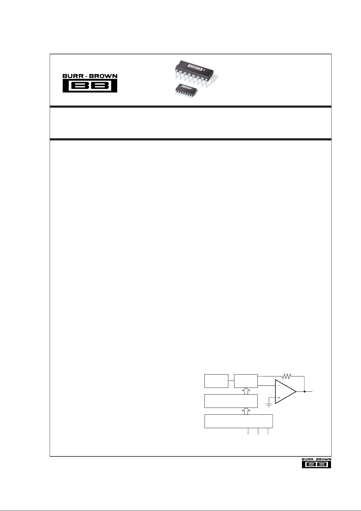
The DAC56 is a complete 16-bit monolithic D/A
converter. Completely self-contained with a stable,
low noise, internal zener voltage reference; high-speed
current switches; a resistor ladder network; and a low
noise output operational amplifier all on a single
monolithic chip. The DAC56 operates over a wide
power supply range from ±5V to ±12V.
Differential linearity error (DLE) is guaranteed to
meet specifications without external adjustment. However, provisions for an externally adjustable circuit
controlling the MSB error, the differential linearity
error at bipolar zero, makes the DLE at BPZ essentially zero and provides for high system performance.
The I/V amplifier stage includes an output current
limiting circuit to protect both amplifier and load from
excessive current. This assures the user of high system
reliability.
A high-speed interface is capable of clocking in data
at a rate of 10MHz max, and its interface logic contains a serial data clock (input), serial data (input) and
latch-enable (input). Serial data is clocked MSB first
into a 16-bit register and then latched into a 16-bit
parallel register.
The DAC56 is packaged in a 16-pin plastic DIP and
16-pin SOIC.
R
F
Output
Reference
16-Bit
I
OUT
DAC
16-Bit Input Latch
16-Bit Serial-to-Parallel Conversion
Clock LE Data
APPLICATIONS
● PROCESS CONTROL
●
ATE PIN ELECTRONICS LEVEL SETTING
● CLOSED-LOOP SERVO-CONTROL
●
AUTO-CALIBRATION CIRCUIT FOR A/D
BOARDS
●
UP-GRADE REPLACEMENT FOR
MULTIPLYING D/A
●
X-Y PLOTTER
●
DSP PROCESSOR BOARDS
PDS-1231A
®
International Airport Industrial Park • Mailing Address: PO Box 11400, Tucson, AZ 85734 • Street Address: 6730 S. Tucson Blvd., Tucson, AZ 85706 • Tel: (520) 746-1111 • Twx: 910-952-1111
Internet: http://www.burr-brown.com/ • FAXLine: (800) 548-6133 (US/Canada Only) • Cable: BBRCORP • Telex: 066-6491 • FAX: (520) 889-1510 • Immediate Product Info: (800) 548-6132
DAC56
DAC56

®
DAC56
2
SPECIFICATIONS
ELECTRICAL
All specifications at +25°C, and power supply voltage of ±5V, unless otherwise noted.
DAC56
PARAMETER CONDITIONS MIN TYP MAX UNITS
DIGITAL INPUT
Resolution 16 Bits
Digital Input Level:
(1)
V
IH
+2.4 +V
L
V
V
IL
0 +0.8 V
I
IH
• VI = +2.7V +1 µA
I
IL
• VI = +0.4V –50 µA
Input Clock Frequency 10 MHz
ACCURACY
Integral Linearity Error ±0.012 % of FSR
(3)
Differential Linearity Error ±0.024 % of FSR
Gain Error ±1.5 % of FSR
Bipolar Zero Error ±0.5 % of FSR
Monotonicity 0°C to +70°C 12 Bits
TEMPERATURE DRIFT 0°C to +70°C
Gain Drift ±60 ppm of FSR/°C
Bipolar Zero Drift ±20 ppm of FSR/°C
Linearity Drift ±0.012 % of FSR
Differential Linearity Drift ±0.024 % of FSR
POWER SUPPLY SENSITIVITY ±V
S
= ±VL = ±5VDC
Gain ±0.0045 % of FSR/%V
Bipolar Zero ±0.0015 % of FSR/%V
SETTLING TIME to ±0.006% of FSR
Voltage Output
6V Step 1.5 µs
1LSB 1 µs
Current Output
1mA Step 10 to 100Ω Load 350 ns
1kΩ Load
(3)
350 ns
Slew Rate 12 V/µs
ANALOG OUTPUT
Voltage Output Configuration
Bipolar Range ±2.66 ±3.0 ±3.34 V
Output Current ±8mA
Output Impedance 0.1 Ω
Short Circuit Duration Indefinite to Common
Current Output Configuration
Bipolar Range ±1mA
Output Impedance 1.2 kΩ
WARMUP TIME 1 min
POWER SUPPLY REQUIREMENTS
(4)
Supply Voltage
+V
S
and +V
L
+4.75 +5.00 +13.2 V
–V
S
and –V
L
–4.75 –5.00 –13.2 V
Supply Drain (No Load)
+V (+V
S
and +VL = +5V) +10 +17 mA
–V (–V
S
and –VL = –5V) –25 –35 mA
+V (+V
S
and +VL = +12V) +12 mA
–V (–V
S
and –VL = –12V) –27 mA
Power Dissipation
V
S
and VL = ±5V 175 260 mW
V
S
and VL = ±12V 468 mW
TEMPERATURE RANGE
Specification 070°C
Storage –60 100 °C
NOTES: (1) Logic input levels are TTL-/CMOS-compatible. (2) FSR means full-scale range and is equivalent to 6V (±3V) for DAC56 in the V
OUT
mode. (3) Measured
with an active clamp to provide a low impedance for approximately 200ns. (4) All specifications assume +V
S
connected to +VL and –VS connected to –VL. If supplies
are connected separately, –V
L
must not be more negative than –VS to assure proper operation. No similar restriction applies to the value of +VL with respect to +VS.
 Loading...