Burr Brown Corporation DAC4813 Datasheet

®
DAC4813
DAC4813
QUAD 12-BIT DIGITAL-TO-ANALOG
CONVERTER (12-bit port interface)
FEATURES
● COMPLETE WITH REFERENCE AND
OUTPUT AMPLIFIERS
● 12-BIT PORT INTERFACE
● ANALOG OUTPUT RANGE:
● MONOTONICITY GUARANTEED OVER
TEMPERATURE
● INTEGRAL LINEARITY
ERROR:
±12V to ±15V SUPPLIES
●
±1/2LSB max
● 28-PIN PLASTIC DIP PACKAGE
10V
Reference
D/A 1
D/A 2
DB0
DAC4813
LSB
±10V
V
REF OUT
V
OUT 1
V
OUT 2
DESCRIPTION
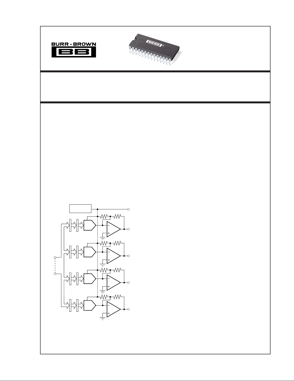
DAC4813 is a complete quad 12-bit digital-to-analog
converter with bus interface logic. Each package includes a precision +10V voltage reference, doublebuffered bus interface including a RESET function
and 12-bit D/A converters with voltage-output operational amplifiers.
The double-buffered interface consists of a 12-bit
input latch and a D/A latch for each D/A converter. A
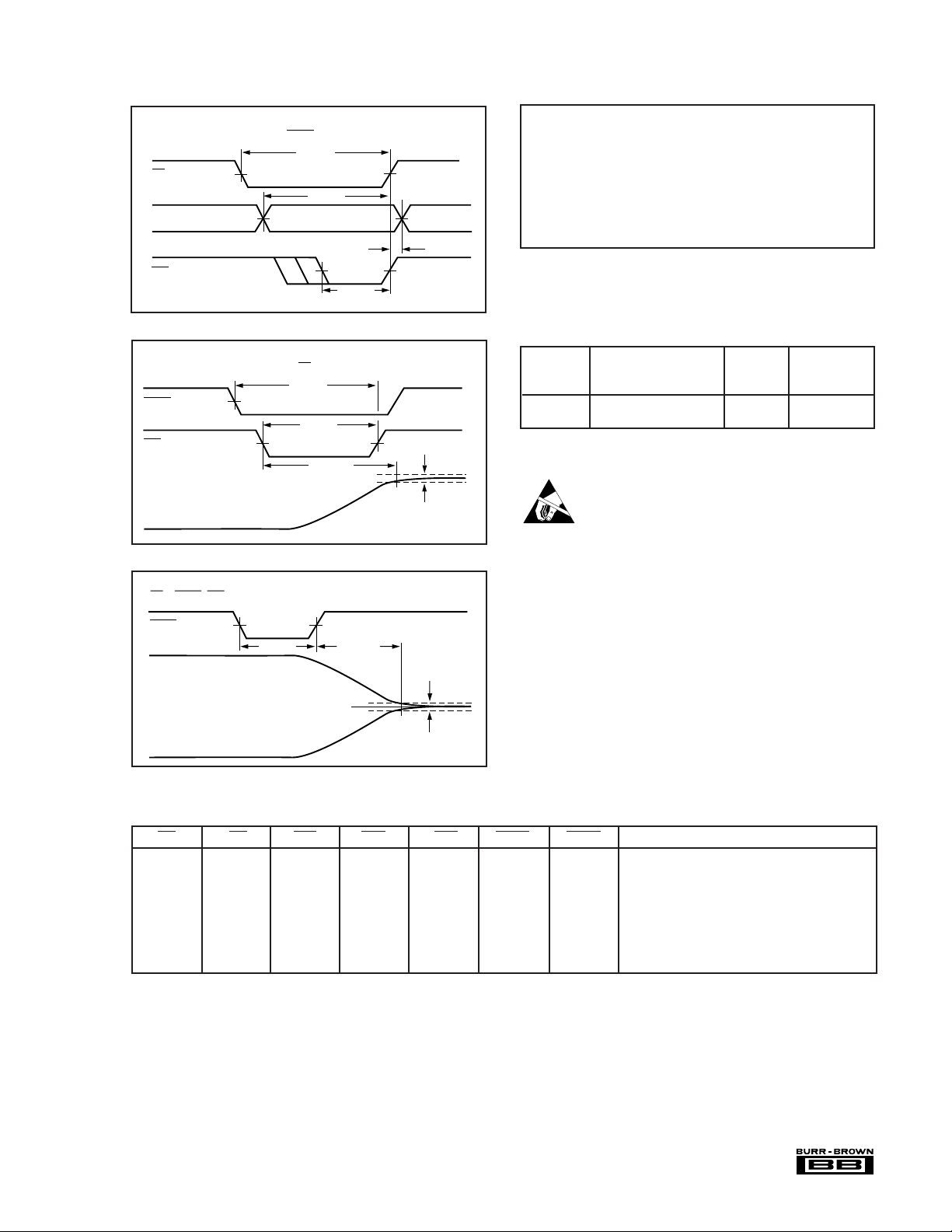
RESET control allows the D/A outputs to be asynchronously reset to bipolar zero, a feature useful for
power-up reset, system initialization and recalibration.
DAC4813 D/A converters are committed to the ±10V
output range only. Gain and offset are not externally
adjustable.
DAC4813 is available with a integral linearity error of
1/2LSB and 12-bit monotonicity guaranteed over temperature. It is packaged in a 28-pin 0.6in. wide plastic
DIP package and specified over –40
0°C to +70°C.
o
C to +85oC and
12-bit
12
Latches
DB11
MSB
International Airport Industrial Park • Mailing Address: PO Box 11400, Tucson, AZ 85734 • Street Address: 6730 S. Tucson Blvd., Tucson, AZ 85706 • Tel: (520) 746-1111 • Twx: 910-952-1111
Internet: http://www.burr-brown.com/ • FAXLine: (800) 548-6133 (US/Canada Only) • Cable: BBRCORP • Telex: 066-6491 • FAX: (520) 889-1510 • Immediate Product Info: (800) 548-6132
© 1992 Burr-Brown Corporation PDS-1148C Printed in U.S.A. May, 1997
D/A 3
D/A 4
V
V
OUT 3
OUT 4
®
1
DAC4813

SPECIFICATIONS
ELECTRICAL
TA = +25oC, +VCC = +12V or +15V, –VCC = –12V or –15V, unless otherwise noted.
DAC4813AP, JP
PARAMETER CONDITIONS MIN TYP MAX UNITS
INPUTS
DIGITAL INPUTS Over Temperature
Input Code
Logic Levels
V
V
Logic Input Currents
DB0-DB11, WR, LDAC, RESET,EN
I
IH
I
IL
(1)
(2)
(3)
IH
IL
X
TRANSFER CHARACTERISTICS
ACCURACY
Linearity Error ±1/4 ±1/2 LSB
Differential Linearity Error ±1/2 ±1 LSB
Gain Error ±0.05 ±0.2 %
Bipolar Zero Error
(5)
Power Supply Sensitivity
Of Full Scale +V
–V
CC
CC
DRIFT Over Specification
Gain ±5 ±30 ppm/°C
Bipolar Zero Drift ±5 ±15 ppmFSR/°C
Linearity Error over Temperature ±1/2 ±3/4 LSB
Monotonicity Guaranteed
DYNAMIC CHARACTERISTICS
SETTLING TIME
Full Scale Range Change 20V Range 4.5 6 µs
1LSB Output Step
Slew Rate 10 V/µs
Crosstalk
(6)
(7)
At Major Carry 2 µs
(8)
OUTPUT
Output Voltage Range ±V
Output Current ±5mA
Output Impedance 0.2 Ω
Short Circuit to ACOM Duration at DC Indefinite
REFERENCE VOLTAGE
Voltage +9.95 +10.00 +10.05 V
Source Current Available
for External Loads 2 mA
Impedance 0.2 Ω
Temperature Coefficient ±5 ±25 ppm/°C
Short Circuit to Common Duration at DC Indefinite
POWER SUPPLY REQUIREMENTS
Voltage:+V
Current: No Load
+V
–V
Power Dissipation 1080 1320 mW
Potential at DCOM with
Respect to ACOM
–V
CC
CC
CC
CC
(9)
TEMPERATURE RANGES
Specification: AP –40 +85 °C
JP 0 +70 °C
Storage –60 +100 °C
Thermal Resistance,
θ
,Plastic DIP 30 °C/W
JA
NOTES: (1) For Two’s Complement Input Coding invert the MSB with an external logic inverter. (2) Digital inputs are TTL and +5V CMOS compatible over the specification
temperature range. (3) Open DATA input lines will be pulled above +5.5V. See discussion under LOGIC INPUT COMPATIBILITY in the OPERATION section. (4) FSR
means Full Scale Range. For example, for ±10V output, FSR = 20V. (5) Error at input code 800
parameter. (7) For the worst-case code change: 7FF
output being driven from –10V to +10V at rated output current. (9) The maximum voltage at which ACOM and DCOM may be separated without affecting accuracy
specifications.
Range Bipolar Offset Binary
+2 +5.5 V
0 +0.8 V
V
= +2.7V ±40 µA
I
V
= +0.4V ±40 µA
I
±0.05 ±0.2 %FSR
±5 ±20 ppmFSR/%+V
±1 ±10 ppmFSR/%–V
Temperature Range
To within ±0.012%FSR
of Final Value
5kΩ || 500pF Load
5kΩ Loads 0.2 LSB
≥ ±11.4V ±10 V
CC
+11.4 +15 +16.5 V
–11.4 –15 –16.5 V
±V
= ±15V
CC
48 60 mA
24 28 mA
–3 +3 V
. (6) Maximum represents the 3σ limit. Not 100% tested for this
HEX
to 800
HEX
and 800
HEX
to 7FF
HEX
HEX
. (8) Crosstalk is defined as the change in any output as a result of any other
(4)
CC
CC
®
DAC4813
2

TIMING DIAGRAMS
WRITE CYCLE #1
(Load first rank from Data Bus: LDAC = 1)
EN
X
DB11–DB0
WR
WRITE CYCLE #2
(Load second rank from first rank: EN
> 50ns
LDAC
WR
V
OUT
> 50ns
> 50ns
= 1)
X
> 50ns
t
SETTLING
> 50ns
> 5ns
±1/2LSB
ABSOLUTE MAXIMUM RATINGS
+VCC to ACOM ............................................................................0 to +18V
–V
to ACOM ............................................................................ 0 to –18V
CC
+V
to –VCC...............................................................................0 to +36V
CC
ACOM to DCOM .................................................................................. ±4V
Digital Inputs to DCOM ...........................................................–1V to +V
External Voltage applied to BPO Resistor ......................................... ±18V
V
.............................................................. Indefinite short to ACOM
REF OUT
V
............................................................................ Momentary to ±18V
OUT
Lead Temperature, soldering 10s .................................................. +300
Max Junction Temperature .............................................................. 165
NOTE: Stresses above those listed under “Absolute Maximum Ratings” may
cause permanent damage to the device. Exposure to absolute maximum
conditions for extended periods may affect device reliability.
CC
o
C
o
C
PACKAGE/ORDERING INFORMATION
PACKAGE
DRAWING TEMPERATURE
PRODUCT PACKAGE NUMBER
DAC4813AP 28-Pin Plastic DBL Wide DIP 215 –40°C to +85°C
DAC4813JP 28-Pin Plastic DBL Wide DIP 215 0°C to +70°C
NOTE: (1) For detailed drawing and dimension table, please see end of data
sheet, or Appendix C of Burr-Brown IC Data Book.
(1)
RANGE
ELECTROSTATIC
DISCHARGE SENSITIVITY
Electrostatic discharge can cause damage ranging from performance degradation to complete device failure. Burr-Brown
RESET COMMAND (Bipolar Mode)
EN
, LDAC, WR = Don’t Care
X
Reset
+10V
V
OUT
–10V
> 50ns
t
SETTLING
0V
±1/2LSB
Corporation recommends that all integrated circuits be handled
and stored using appropriate ESD protection methods.
TRUTH TABLE
WR EN1 EN2 EN3 EN4 LDAC RESET OPERATION
X X X X X X 0 Reset all D/A Latches
1 X X X X X 1 No Operation
X 1 1 1 1 1 1 No Operation
0 1 1 1 0 1 1 Load Data into First Rank for D/A 4
0 1 1 0 1 1 1 Load Data into First Rank for D/A 3
0 1 0 1 1 1 1 Load Data into First Rank for D/A 2
0 0 1 1 1 1 1 Load Data into First Rank for D/A 1
0 1 1 1 1 0 1 Load Second Rank from First Rank, All D/As
0 0 0 0 0 0 1 All Latches Transparent
“X” = Don’t Care
®
3
DAC4813
 Loading...