®
For most current data sheet and other product
information, visit www.burr-brown.com
20-Bit Low Power
DIGITAL-TO-ANALOG CONVERTER
DAC1220
DAC1220
FEATURES
● 20-BIT MONOTONICITY GUARANTEED
OVER –40°C to +85°C
● LOW POWER: 2.5mW
● VOLTAGE OUTPUT
● SETTLING TIME: 2ms to 0.012%
● MAX LINEARITY ERROR: ±0.0015%
● ON-CHIP CALIBRATION
DESCRIPTION
The DAC1220 is a 20-bit digital-to-analog (D/A)
converter offering 20-bit monotonic performance over
the specified temperature range. It utilizes delta-sigma
technology to achieve inherently linear performance
in a small package at very-low power. The resolution
of the device can be programmed to 20 bits for fullscale, settling to 0.003% within 15ms typical, or 16
bits for full-scale, settling to 0.012% within 2ms max.
The output range is two times the external reference
voltage. On-chip calibration circuitry dramatically reduces low offset and gain errors.
APPLICATIONS
● PROCESS CONTROL
● ATE PIN ELECTRONICS
● CLOSED-LOOP SERVO-CONTROL
● SMART TRANSMITTERS
● PORTABLE INSTRUMENTS
The DAC1220 features a synchronous serial interface.
In single-converter applications, the serial interface
can be accomplished with just two wires, allowing
low-cost isolation. For multiple converters, a CS signal
allows for selection of the appropriate D/A converter.
The DAC1220 has been designed for closed-loop
control applications in the industrial process control
market and high-resolution applications in the test and
measurement market. It is also ideal for remote applications, battery-powered instruments, and isolated systems. The DAC1220 is available in a SSOP-16
package.
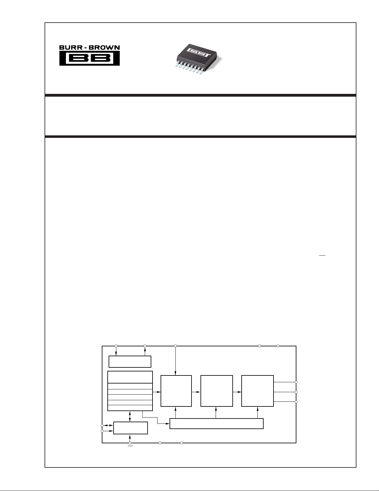
X
IN
Clock Generator
Microcontroller
Instruction Register
Command Register
Data Register
Offset Register
Full-Scale Register
SDIO
SCLK
International Airport Industrial Park • Mailing Address: PO Box 11400, Tucson, AZ 85734 • Street Address: 6730 S. Tucson Blvd., Tucson, AZ 85706 • Tel: (520) 746-1111
Twx: 910-952-1111 • Internet: http://www.burr-brown.com/ • Cable: BBRCORP • Telex: 066-6491 • FAX: (520) 889-1510 • Immediate Product Info: (800) 548-6132
© 1998 Burr-Brown Corporation PDS-1418B Printed in U.S.A. April , 2000
X
OUT
Serial
Interface
CS DV
V
REF
Second-Order
∆∑
Modulator
DGND
DD
First-Order
Switched
Capacitor Filter
Modulator Control
1
AVDDAGND
Second-Order
Continuous
Time Post Filter
C
1
V
OUT
C
2
®

SPECIFICATIONS
All specifications T
PARAMETER CONDITIONS MIN TYP MAX UNITS
ACCURACY
Monotonicity 16 Bits
Monotonicity 20-Bit Mode 20 Bits
Linearity Error ±1
Unipolar Offset Error
Unipolar Offset Error Drift
Bipolar Zero Offset Error
Bipolar Zero Offset Drift
Gain Error
Gain Error Drift
Power Supply Rejection Ratio at DC, dB = –20log(∆V
ANALOG OUTPUT
Output Voltage
Output Current 0.5 mA
Capacitive Load 500 pF
Short-Circuit Current ±20 mA
Short-Circuit Duration GND or V
DYNAMIC PERFORMANCE
Settling Time
Output Noise Voltage 0.1Hz to 10Hz 1 µVrms
REFERENCE INPUT
Input Voltage 2.25 2.5 2.75 V
Input Impedance 100 kΩ
DIGITAL INPUT/OUTPUT
Logic Family TTL-Compatible CMOS
Logic Levels (all except X
V
IH
V
IL
V
OH
V
OL
Input-Leakage Current ±10 µA
XIN Frequency Range (f
Data Format User Programmable Offset Two’s Complement
POWER SUPPLY REQUIREMENTS
Power Supply Voltage 4.75 5.25 V
Supply Current
Analog Current 360 µA
Digital Current 140 µA
Analog Current 20-Bit Mode 460 µA
Digital Current 20-Bit Mode 140 µA
Power Dissipation 2.5 3.5 mW
TEMPERATURE RANGE
Specified Performance –40 +85 °C
NOTES: (1) Valid from AGND + 20mV to AV
(4) Ideal output voltage, does not take into account gain and offset error. (5) Valid from AGND +20mV to AV
be twice the value indicated. For 16-bit mode, C
to T
MIN
, AVDD = DVDD = +5V, f
MAX
= 2.5MHz, V
XIN
= +2.5V, and 16-bit mode, unless otherwise noted.
REF
DAC1220E
(1)
(2)
(3)
(2)
(3)
(2)
(3)
(4)
(5)
V
= 20mV ±4 LSB
OUT
1 ppm/°C
V
OUT
= V
REF
±1 LSB
1 ppm/°C
±10 LSB
2 ppm/°C
/∆VDD)60dB
OUT
0 2 • V
DD
Indefinite
REF
To ±0.012% 1.8 2 ms
20-Bit Mode, to ±0.003% 15 ms
)
IN
2.0 DVDD +0.3 V
–0.3 0.8 V
IOH = –0.8mA 3.6 V
IOL = 1.6mA 0.4 V
) 0.5 2.5 MHz
XIN
or Straight Binary
20-Bit Mode 3.0 mW
Sleep Mode 0.45 mW
– 20mV, in the 16-bit mode. (2) Applies after calibration, in 16-bit mode. (3) Re-calibration can remove these errors.
DD
= 2.2nF, C2 = 0.22nF; for 20-bit mode, C1 = 10nF, C2 = 3.3nF.
1
–20mV. Outside of this range, settling time may
DD
LSB
V
®
DAC1220
2

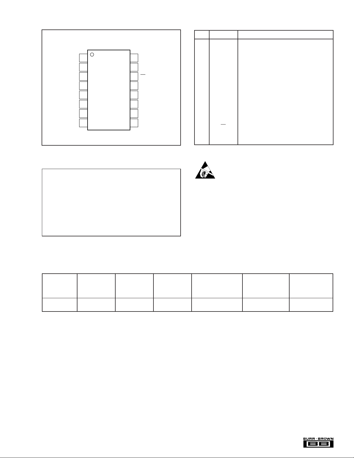
PIN CONFIGURATION
PIN DESCRIPTIONS
Top View SSOP
DV
1
DD
X
2
OUT
X
3
IN
4
DGND
AV
DNC
DNC
DNC
DD
DAC1220E
5
6
7
8
ABSOLUTE MAXIMUM RATINGS
AV
to DVDD................................................................................... ±0.3V
DD
to AGND ........................................................................ –0.3V to 6V
AV
DD
to DGND ....................................................................... –0.3V to 6V
DV
DD
AGND to DGND ............................................................................... ±0.3V
Voltage to AGND .......................................................... 2.0V to 3.0V
V
REF
Digital Input Voltage to DGND .............................. –0.3V to DV
Digital Output Voltage to DGND ........................... –0.3V to DV
Package Power Dissipation ............................................. (T
Maximum Junction Temperature (T
Thermal Resistance,
SSOP-16................................................................................ 200°C/W
Lead Temperature (soldering, 10s) ............................................... +300°C
NOTE: (1) Stresses above those listed under “Absolute Maximum Ratings”
may cause permanent damage to the device. Exposure to absolute maximum
conditions for extended periods may affect device reliability.
θ
JA
) ..................................... +150°C
JMAX
SCLK
16
SDIO
15
CS
14
AGND
13
V
12
REF
11
V
OUT
C
10
2
9
C
1
(1)
+ 0.3V
DD
+ 0.3V
DD
– TA)/
JMAX
θ
JA
PIN NAME DESCRIPTION
1DV
2X
3X
4 DGND Digital Ground
5AV
6 DNC Do Not Connect
7 DNC Do Not Connect
8 DNC Do Not Connect
9C
10 C
11 V
12 V
13 AGND Analog Ground
14 CS Chip Select Input
15 SDIO Serial Data Input/Output
16 SCLK Clock Input for Serial Data Transfer
OUT
IN
OUT
REF
Digital Supply, +5V nominal
DD
System Clock Output (for Crystal)
System Clock Input
Analog Supply, +5V nominal
DD
Filter Capacitor, see text.
1
Filter Capacitor, see text.
2
Analog Output Voltage
Reference Input
ELECTROSTATIC
DISCHARGE SENSITIVITY
This integrated circuit can be damaged by ESD. Burr-Brown
recommends that all integrated circuits be handled with
appropriate precautions. Failure to observe proper handling
and installation procedures can cause damage.
ESD damage can range from subtle performance degradation
to complete device failure. Precision integrated circuits may
be more susceptible to damage because very small parametric
changes could cause the device not to meet its published
specifications.
PACKAGE/ORDERING INFORMATION
MAXIMUM
LINEARITY PACKAGE SPECIFICATION
PRODUCT (LSB) PACKAGE NUMBER RANGE NUMBER
ERROR DRAWING TEMPERATURE ORDERING TRANSPORT
DAC1220E ±1 SSOP-16 322 –40°C to +85°C DAC1220E Rails
"""" "DAC1220E/2K5 Tape and Reel
NOTE: (1) Models with a slash (/) are available only in Tape and Reel in the quantities indicated (e.g., /2K5 indicates 2500 devices per reel). Ordering 2500 pieces
of “DAC1220E/2K5” will get a single 2500-piece Tape and Reel.
The information provided herein is believed to be reliable; however, BURR-BROWN assumes no responsibility for inaccuracies or omissions. BURR-BROWN assumes
no responsibility for the use of this information, and all use of such information shall be entirely at the user’s own risk. Prices and specifications are subject to change
without notice. No patent rights or licenses to any of the circuits described herein are implied or granted to any third party. BURR-BROWN does not authorize or warrant
any BURR-BROWN product for use in life support devices and/or systems.
(1)
MEDIA
®
3

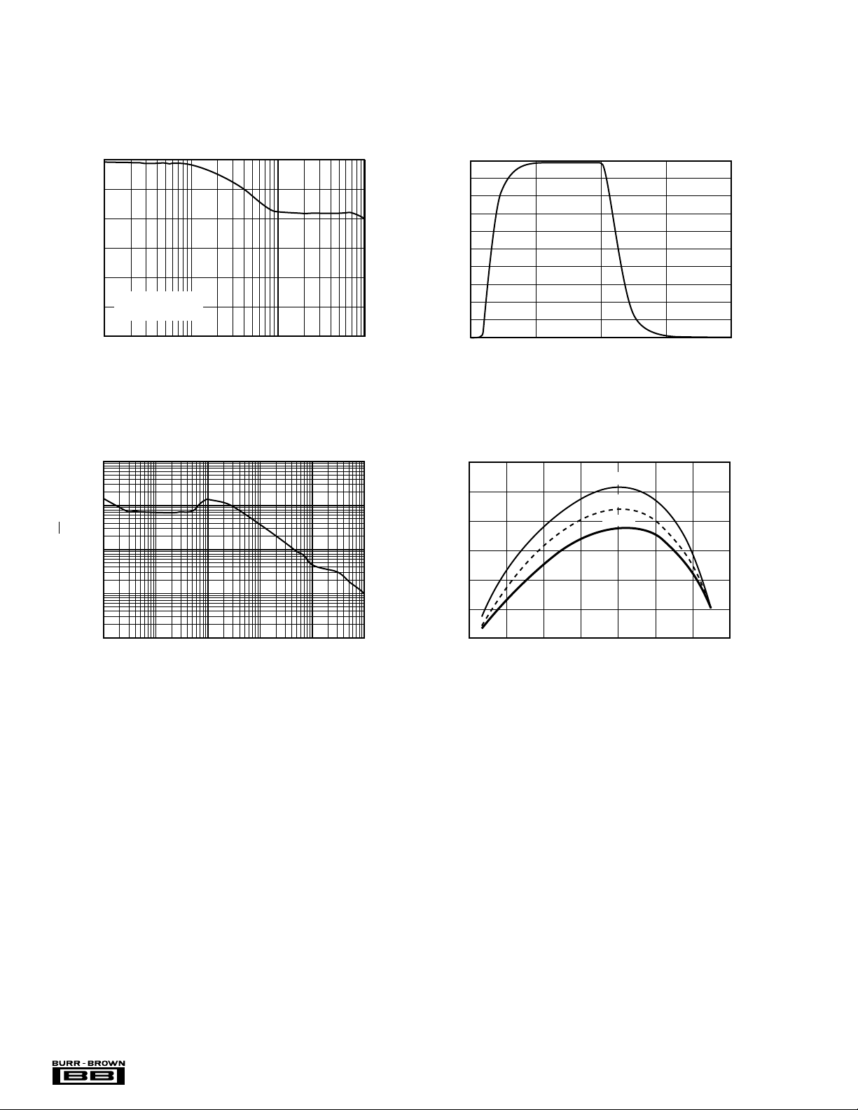
TYPICAL PERFORMANCE CURVES
At TA = +25°C, AVDD = DVDD = +5.0V, f
POWER SUPPLY REJECTION RATIO vs FREQUENCY
60
50
40
30
PSRR (dB)
20
400mVp-p Ripple
10
Mid-Range Output
0
10 100 1k 10k
Frequency (Hz)
OUTPUT NOISE VOLTAGE vs FREQUENCY
10k
1k
= 2.5MHz, V
XIN
= 2.5V, C1 = 2.2nF and C2 = 0.22nF, calibrated mode, unless otherwise specified.
REF
5.0
4.5
4.0
3.5
3.0
2.5
(V)
2.0
1.5
1.0
0.5
0.0
01234
10
8
6
LARGE-SIGNAL SETTLING TIME
Time (ms)
LINEARITY ERROR vs CODE
–40°C
+25°C
+85°C
100
Noise (nV/√Hz)
10
1
10 100 1k 10k 100k 1M
Frequency (Hz)
4
2
Linearity Error (ppm)
0
–2
0
10000 20000 30000 40000 50000 60000 70000
Code
®
DAC1220
4

THEORY OF OPERATION
The DAC1220 is a precision, high dynamic range, selfcalibrating, 20-bit, delta-sigma digital-to-analog converter.
It contains a second-order delta-sigma modulator, a firstorder switched-capacitor filter, a second-order continuoustime post filter, a microcontroller including the Instruction,
Command and Calibration registers, a serial interface, and a
clock generator circuit.
The design topology provides low system noise and good
power-supply rejection. The modulator frequency of the
delta-sigma D/A converter is controlled by the system clock.
The DAC1220 also includes complete onboard calibration
that can correct for internal offset and gain errors.
The calibration registers are fully readable and writable.
This feature allows for system calibration. The various
settings, modes, and registers of the DAC1220 are read or
written via a synchronous serial interface. This interface
operates as an externally clocked interface.
DEFINITION OF TERMS
Differential Nonlinearity Error—The differential
nonlinearity error is the difference between an actual step
width and the ideal value of 1 LSB. If the step width is
exactly 1 LSB, the differential nonlinearity error is zero.
A differential nonlinearity specification of less than 1 LSB
guarantees monotonicity.
Drift—The drift is the change in a parameter over temperature.
Full-Scale Range (FSR)—This is the magnitude of the
typical analog output voltage range which is 2 • V
For example, when the converter is configured with a 2.5V
reference, the full-scale range is 5.0V.
Gain Error—This error represents the difference in the
slope between the actual and ideal transfer functions.
Linearity Error—The linearity error is the deviation of the
actual transfer function from an ideal straight line between
the data end points.
Least Significant Bit (LSB) Weight—This is the ideal
change in voltage that the analog output will change with a
change in the digital input code of 1 LSB.
Monotonicity—Monotonicity assures that the analog output will increase or stay the same for increasing digital input
codes.
Offset Error—The offset error is the difference between
the expected and actual output, when the output is zero. The
value is calculated from measurements made when
V
= 20mV.
OUT
Settling Time—The settling time is the time it takes the
output to settle to its new value after the digital code has
been changed.
f
—The frequency of the crystal oscillator or CMOS-
XIN
compatible input signal at the XIN input of the DAC1220.
REF
ANALOG OPERATION
The system clock is divided down to provide the sample
clock for the modulator. The sample clock is used by the
modulator to convert the multi-bit digital input into a one-bit
digital output stream. The use of a 1-bit DAC provides
inherent linearity. The digital output stream is then converted into an analog signal via the 1-bit DAC and then
filtered by the 1st-order switched capacitor filter.
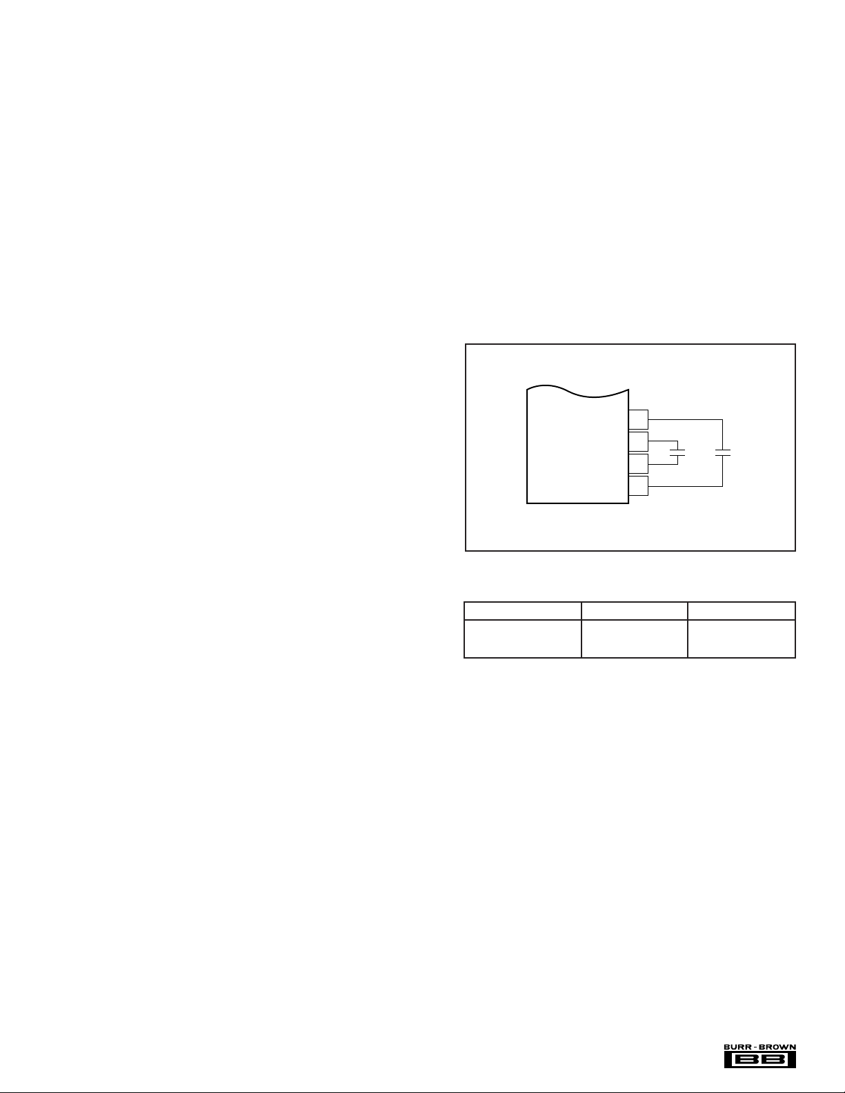
The output of the switched-capacitor filter feeds into the
continuous time filter. The continuous time filter uses external capacitors connected between the C1, C2, V
V
pins to adjust the settling time. The connections for the
OUT
capacitors are shown in Figure 1 (C1 connects between the
V
and C1 pins, and C2 connects between the V
REF
pins).
DAC1220
FIGURE 1. External Capacitor Connections.
.
CAPACITOR 16-BIT MODE 20-BIT MODE
C
1
C
2
TABLE I. External Capacitor Values.
CALIBRATION
The DAC1220 offers a self-calibration mode which automatically calibrates the output offset and gain. The calibration is performed once and then normal operation is resumed. In general, calibration is recommended immediately
after power-on and whenever there is a “significant” change
in the operating environment. The amount of change which
should cause a re-calibration is dependent on the application. Where high accuracy is important, re-calibration should
be done on changes in temperature and power supply.
After a calibration has been accomplished, the Offset Calibration Register (OCR) and the Full-Scale Calibration Register (FCR) contain the results of the calibration.
Note that the values in the calibration registers will vary
from configuration-to-configuration and from part to part.
V
12
REF
V
11
OUT
C
10
2
C
9
1
2.2nF 10nF
0.22nF 3.3nF
C
2
OUT
C
1
REF
and C
, and
2
®
5
 Loading...