Burr Brown Corporation BUF601AU-2K5, BUF601, BUF600AU, BUF600 Datasheet
1
®
BUF600, 601
HIGH-SPEED BUFFER AMPLIFIER
FEATURES
● OPEN-LOOP BUFFER
● HIGH-SLEW RATE: 3600V/
µs, 5.0Vp-p
● BANDWIDTH: 320MHz, 5.0Vp-p
900MHz, 0.2Vp-p
● LOW INPUT BIAS CURRENT: 0.7
µA/1.5µA
● LOW QUIESCENT CURRENT: 3mA/6mA
● GAIN FLATNESS: 0.1dB, 0 to 300MHz
The BUF601, with 6mA quiescent current and therefore lower output impedance, can easily drive 50Ω
inputs or 75Ω systems and cables.
The broad range of analog and digital applications
extends from decoupling of signal processing stages,
impedance transformation, and input amplifiers for
RF equipment and ATE systems to video systems,
distribution fields, IF/communications systems, and
output drivers for graphic cards.
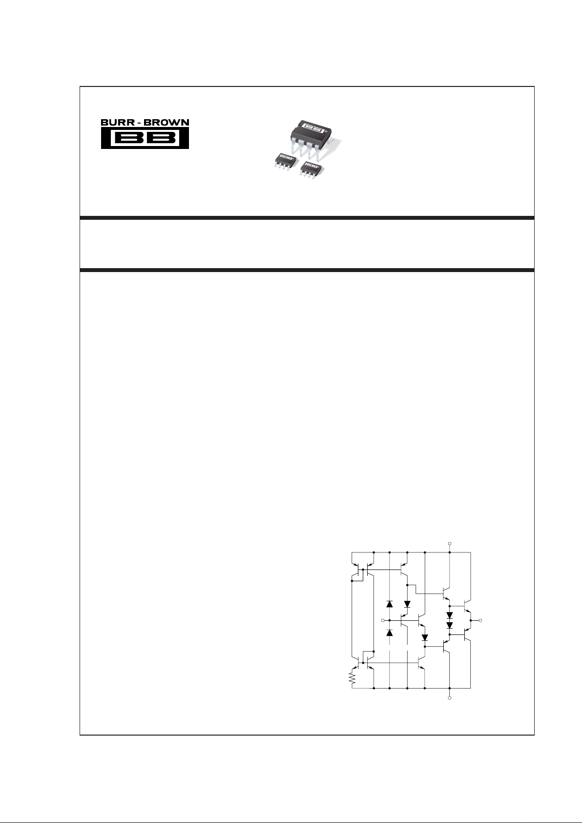
V+ = +5V
(1)
Bias
Circuitry
V
OUT
(8)
V
IN
(4)
V– = –5V
(5)
BUFFER
Simplified Circuit Diagram
BUF600
BUF601
®
DESCRIPTION
The BUF600 and BUF601 are monolithic open-loop
unity-gain buffer amplifiers with a high symmetrical
slew rate of up to 3600V/µs and a very wide bandwidth of 320MHz at 5Vp-p output swing. They use a
complementary bipolar IC process, which incorporates pn-junction isolated high-frequency NPN and
PNP transistors to achieve high-frequency performance
previously unattainable with conventional integrated
circuit technology.
Their unique design offers a high-performance alternative to expensive discrete or hybrid solutions.
The BUF600 and BUF601 feature low quiescent
current, low input bias current, small signal delay time
and phase shift, and low differential gain and phase
errors.
The BUF600 with 3mA quiescent current is wellsuited for operation between high-frequency
processing stages. It demonstrates outstanding performance even in feedback loops of wide-band amplifiers
or phase-locked loop systems.
APPLICATIONS
● VIDEO BUFFER/LINE DRIVER
● INPUT/OUTPUT AMPLIFIER FOR
MEASUREMENT EQUIPMENT
● PORTABLE SYSTEMS
● TRANSMISSION SYSTEMS
● TELECOMMUNICATIONS
● HIGH-SPEED ANALOG SIGNAL
PROCESSING
● ULTRASOUND
International Airport Industrial Park • Mailing Address: PO Box 11400, Tucson, AZ 85734 • Street Address: 6730 S. Tucson Blvd., Tucson, AZ 85706 • Tel: (520) 746-1111 • Twx: 910-952-1111
Internet: http://www.burr-brown.com/ • FAXLine: (800) 548-6133 (US/Canada Only) • Cable: BBRCORP • Telex: 066-6491 • FAX: (520) 889-1510 • Immediate Product Info: (800) 548-6132
BUF600
BUF600
BUF601
© 1991 Burr-Brown Corporation PDS-1128F Printed in U.S.A. March, 1998
2
®
BUF600, 601
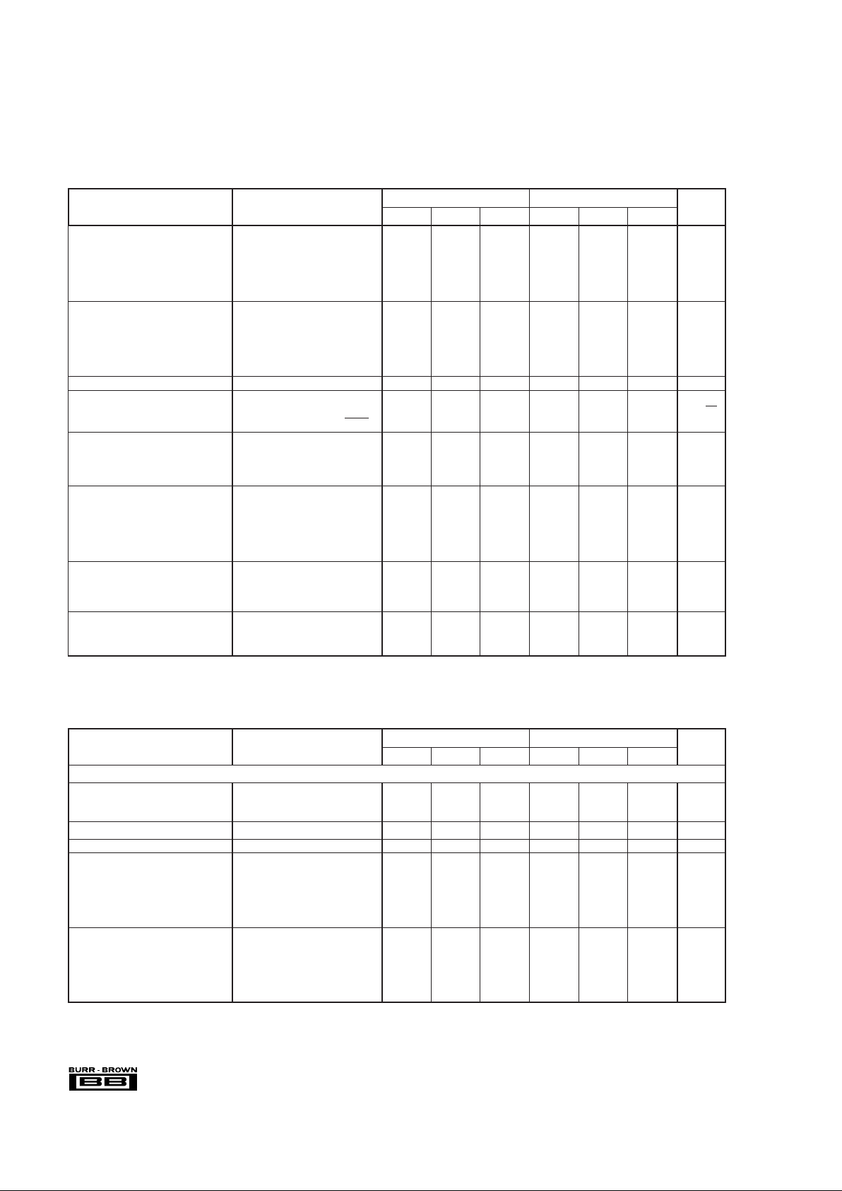
INPUT OFFSET VOLTAGE
Initial ±15 ±30 ±15 ±30 mV
vs Temperature 925µV/°C
vs Supply (tracking) V
CC
= ±4.5V to ±5.5V –54 –72 –54 –77 dB
vs Supply (non-tracking) V
CC
= +4.5V to +5.5V –55 –55 dB
vs Supply (non-tracking) V
CC
= –4.5V to –5.5V –54 –54 dB
INPUT BIAS CURRENT
Initial +3.5 –2.5/+5 +3.5 –5/+10 µA
vs Temperature 0.4 0.7 nA/°C
vs Supply (tracking) V
CC
= ±4.5V to ±5.5V 0.15 0.3 µA/V
vs Supply (non-tracking) V
CC
= +4.5V to +5.5V 0.5 0.5 µA/V
vs Supply (non-tracking) V
CC
= –4.5V to –5.5V 20 20 nA/V
INPUT IMPEDANCE 4.8 || 1 2.5 || 1 MΩ || pF
INPUT NOISE
Voltage Noise Density f = 100kHz to 100MHz 5.2 4.8 nV/√Hz
Signal-to-Noise Ratio S/N = 20 Log (0.7/(Vn • √5MHz)) 95 96 dB
TRANSFER CHARACTERISTICS Voltage Gain; V
IN
= ±2.5V
R
LOAD
= 100Ω 0.95 V/V
R
LOAD
= 200Ω 0.96 V/V
R
LOAD
= 10kΩ 0.99 0.99 V/V
RATED OUTPUT
Voltage Output V
IN
= ±2.7V
R
LOAD
= 100Ω±2.5 ±2.6 V
R
LOAD
= 200Ω±2.5 ±2.6 V
DC Current Output DC, R
LOAD
= 100Ω±20 ±20 mA
Output Impedance 6.2 3.6 Ω
POWER SUPPLY
Rated Voltage ±5 ±5V
Derated Performance ±4.5 ±5.5 ±4.5 ±5.5 V
Quiescent Current ±2.6 ±3 ±3.4 ±5.4 ±6 ±6.6 mA
TEMPERATURE RANGE
Specification –40 85 –40 85 °C
Storage –40 125 –40 125 °C
BUF600AP, AU BUF601AU
PARAMETER CONDITIONS MIN TYP MAX MIN TYP MAX UNITS
AC SPECIFICATION
At VCC = ±5V, R
LOAD
= 200Ω (BUF600) and 100Ω (BUF601), R
SOURCE
= 50Ω, and T
AMB
= +25°C, unless otherwise noted.
FREQUENCY DOMAIN
LARGE SIGNAL BANDWIDTH V
O
= 5Vp-p, C
OUT
= 1pF 320 320 MHz
(–3dB) V
O
= 2.8Vp-p, C
OUT
= 1pF 400 400 MHz
V
O
= 1.4Vp-p, C
OUT
= 1pF 700 700 MHz
SMALL SIGNAL BANDWIDTH V
O
= 0.2Vp-p, C
OUT
= 1pF 650 900 MHz
GROUP DELAY TIME 250 200 ps
DIFFERENTIAL GAIN V
IN
= 0.3Vp-p, f = 4.43MHz
V = 0 to 0.7V
BUF600 R
LOAD
= 200Ω 0.5 %
R
LOAD
= 1kΩ 0.075 %
BUF601 R
LOAD
= 100Ω 0.4 %
R
LOAD
= 500Ω 0.05 %
DIFFERENTIAL PHASE V
IN
= 0.3Vp-p, f = 4.43MHz
V = 0 to 0.7V
BUF600 R
LOAD
= 200Ω 0.02 Degrees
R
LOAD
= 1kΩ 0.04 Degrees
BUF601 R
LOAD
= 100Ω 0.025 Degrees
R
LOAD
= 500Ω 0.03 Degrees
SPECIFICATIONS
DC SPECIFICATION
At VCC = ±5V, R
LOAD
= 10kΩ, R
SOURCE
= 50Ω, and T
AMB
= +25°C, unless otherwise noted.
BUF600AP, AU BUF601AU
PARAMETER CONDITIONS MIN TYP MAX MIN TYP MAX UNITS
3
®
BUF600, 601
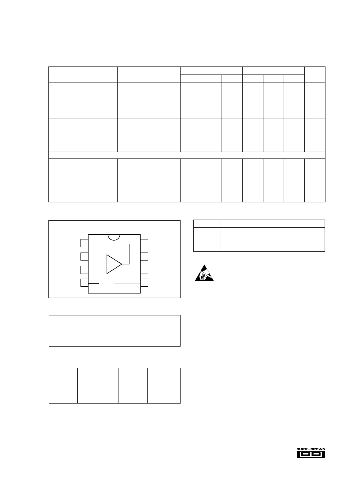
BUF600AP, AU BUF601AU
PARAMETER CONDITIONS MIN TYP MAX MIN TYP MAX UNITS
HARMONIC DISTORTION
Second Harmonic f = 10MHz, V
O
= 1.4Vp-p –65 –65 dBc
Third Harmonic –64 –67 dBc
Second Harmonic f = 30MHz, V
O
= 1.4Vp-p –51 –59 dBc
Third Harmonic –56 –62 dBc
Second Harmonic f = 50MHz, V
O
= 1.4Vp-p –43 –53 dBc
Third Harmonic –48 –54 dBc
GAIN FLATNESS PEAKING
V
O
= 0.4Vp-p, DC to 30MHz 0.01 0.005 dB
V
O
= 0.4Vp-p, 30MHz to 300MHz 0.3 0.1 dB
LINEAR PHASE DEVIATION
V
O
= 0.4Vp-p, DC to 30MHz 5.5 3.8 Degrees
V
O
= 0.4Vp-p, 30 to 300MHz 55 45 Degrees
TIME DOMAIN
RISE TIME 10% to 90%, 700ps
1.4Vp-p Step 0.82 0.87 ns
2.8Vp-p Step 0.97 0.95 ns
5.0Vp-p Step 1.18 1.13 ns
SLEW RATE
V
O
= 1.4Vp-p 1500 1500 V/µs
V
O
= 2.8Vp-p 2400 2400 V/µs
V
O
= 5.0Vp-p 3400 3600 V/µs
AC-SPECIFICATIONS (CONT)
At VCC = ±5V, R
LOAD
= 200Ω (BUF600) and 100Ω (BUF601), R
SOURCE
= 50Ω, and T
AMB
= +25°C, unless otherwise noted.
PIN CONFIGURATION
Top View
DIP/SO-8
FUNCTION DESCRIPTION
In Analog Input
Out Analog Output
+V
CC
Positive Supply Voltage; typical +5VDC
–V
CC
Negative Supply Voltage; typical –5VDC
FUNCTIONAL DESCRIPTION
ELECTROSTATIC
DISCHARGE SENSITIVITY
This integrated circuit can be damaged by ESD. Burr-Brown
recommends that all integrated circuits be handled with
appropriate precautions. Failure to observe proper handling
and installation procedures can cause damage.
ESD damage can range from subtle performance degradation to complete device failure. Precision integrated circuits
may be more susceptible to damage because very small
parametric changes could cause the device not to meet its
published specifications.
Power Supply Voltage.......................................................................... ±6V
Input Voltage
(1)
.........................................................................±VCC ±0.7V
Operating Temperature..................................................... –40°C to +85 °C
Storage Temperature...................................................... –40°C to +125°C
Junction Temperature .................................................................... +150°C
Lead Temperature (soldering, 10s)................................................ +300°C
NOTE: (1) Inputs are internally diode-clamped to ±V
CC.
ABSOLUTE MAXIMUM RATINGS
PACKAGE
DRAWING TEMPERATURE
PRODUCT PACKAGE NUMBER
(1)
RANGE
BUF600AP Plastic 8-Pin DIP 006 –40°C to +85°C
BUF600AU SO-8 Surface Mount 182 –40°C to +85°C
BUF601AU SO-8 Surface Mount 182 –40°C to +85°C
NOTE: (1) For detailed drawing and dimension table, please see end of data
sheet, or Appendix C of Burr-Brown IC Data Book.
PACKAGE/ORDERING INFORMATION
1
2
3
4
8
7
6
5
+V
CC
NC
NC
In
Out
NC
NC
–V
CC
BUF600, BUF601
The information provided herein is believed to be reliable; however, BURR-BROWN assumes no responsibility for inaccuracies or omissions. BURR-BROWN assumes
no responsibility for the use of this information, and all use of such information shall be entirely at the user’s own risk. Prices and specifications are subject to change
without notice. No patent rights or licenses to any of the circuits described herein are implied or granted to any third party. BURR-BROWN does not authorize or warrant
any BURR-BROWN product for use in life support devices and/or systems.
4
®
BUF600, 601
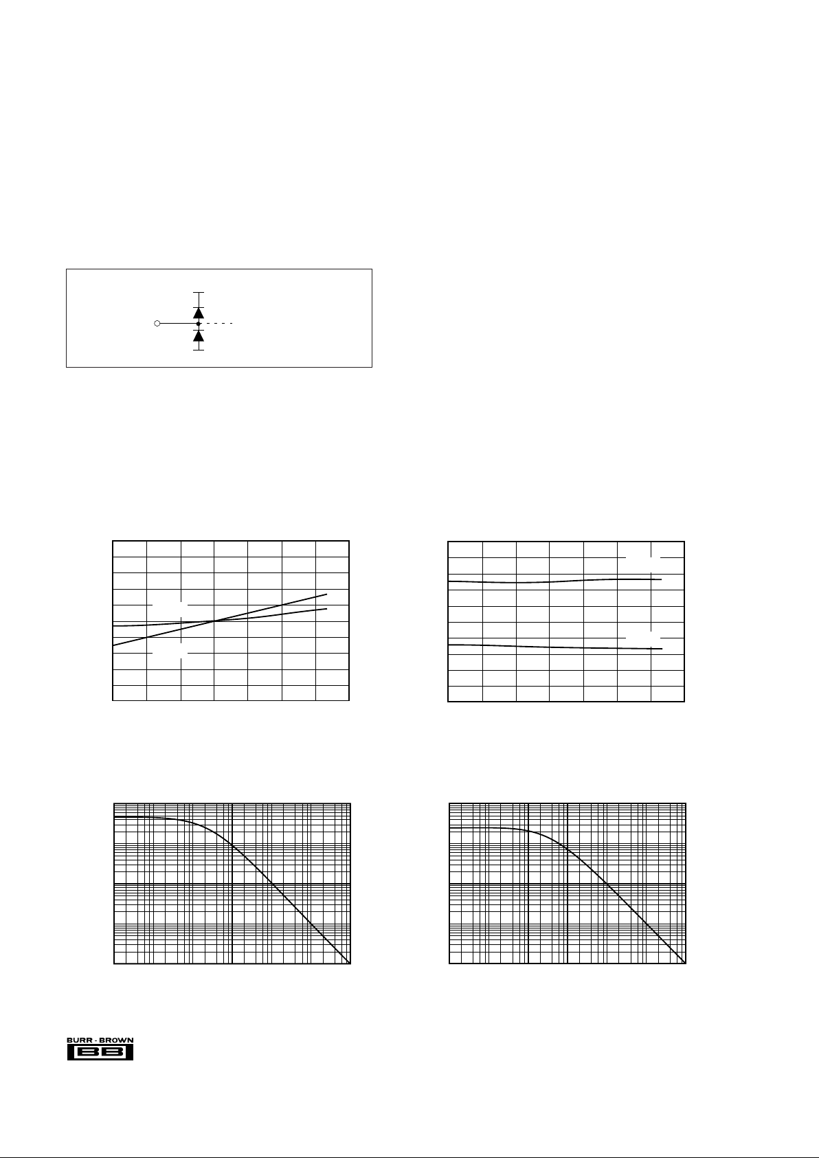
INPUT PROTECTION
Static damage has been well recognized for MOSFET devices, but any semiconductor device deserves protection
from this potentially damaging source. The BUF600 and
BUF601 incorporate on-chip ESD protection diodes as shown
in Figure 1. This eliminates the need for the user to add
external protection diodes, which can add capacitance and
degrade AC performance.
FIGURE 1. Internal ESD Protection.
+V
CC
–V
CC
External
Pin
Internal
Circuitry
ESD Protection Diodes
internally connected to
all pins.
All input pins on the BUF600 and BUF601 are internally
protected from ESD by means of a pair of back-to-back
reverse-biased diodes to the power supplies as shown. These
diodes will begin to conduct when the input voltage exceeds
either power supply by about 0.7V. This situation can occur
with loss of the amplifier’s power supplies while a signal
source is still present. The diodes can typically withstand a
continuous current of 30mA without destruction. To insure
long term reliability, however, the diode current should be
externally limited to 10mA or so whenever possible.
The internal protection diodes are designed to withstand
2.5kV (using the Human Body Model) and will provide
adequate ESD protection for most normal handling procedures. However, static damage can cause subtle changes in
amplifier input characteristics without necessarily destroying the device. In precision amplifiers, this may cause a
noticeable degradation of offset and drift. Therefore, static
protection is strongly recommended when handling the
BUF600 and BUF601.
TYPICAL PERFORMANCE CURVES
At VCC = ±5V, R
LOAD
= 10kΩ, and TA = 25°C, unless otherwise noted.
INPUT BIAS CURRENT vs TEMPERATURE
–40
2
1.8
1.6
1.4
1.2
1
0.8
0.6
0.4
0.2
0
Temperature (°C)
Bias Current (µA)
–200 20406080100
BUF600
BUF601
OFFSET VOLTAGE vs TEMPERATURE
–40
5
4
3
2
1
0
–1
–2
–3
–4
–5
Temperature (°C)
Offset Voltage (mV, normalized)
–200 20406080100
BUF600
BUF601
INPUT IMPEDANCE vs FREQUENCY BUF601
100
10M
1M
100k
10k
1k
Frequency (Hz)
Input Impedance (Ω)
1k 10k 100k 1M 10M 100M
INPUT IMPEDANCE vs FREQUENCY BUF600
100
10M
1M
100k
10k
1k
Frequency (Hz)
Input Impedance (Ω)
1k 10k 100k 1M 10M 100M
5
®
BUF600, 601
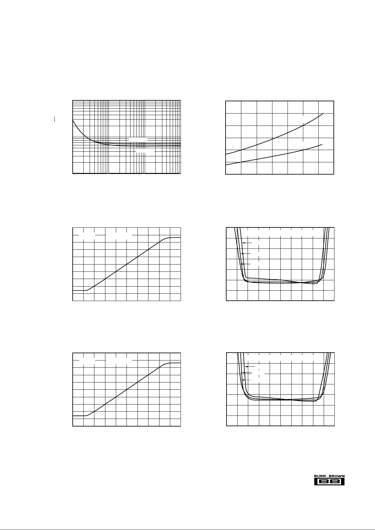
TYPICAL PERFORMANCE CURVES (CONT)
At VCC = ±5V, R
LOAD
= 10kΩ, and TA = 25°C, unless otherwise noted.
BUF601 GAIN ERROR vs INPUT VOLTAGE
–5
14
12
10
8
6
4
2
0
Input Voltage (V)
Gain Error (%)
–4 –3 –2 –1 0 1 2 3 4 5
+85°C
(Full Temperature Range, R
LOAD
= 100Ω)
–40°C
+25°C
BUF601 TRANSFER FUNCTION
–5
5
4
3
2
1
0
–1
–2
–3
–4
–5
Input Voltage (V)
–4–3–2–1012345
Output Voltage (V)
R
LOAD
= 100ΩBUF601
BUF600 GAIN ERROR vs INPUT VOLTAGE
–5
14
12
10
8
6
4
2
0
Input Voltage (V)
Gain Error (%)
–4 –3 –2 –1 0 1 2 3 4 5
85°C
(Full Temperature Range, R
LOAD
= 200Ω)
–40°C
+25°C
BUF600 TRANSFER FUNCTION
–5
5
4
3
2
1
0
–1
–2
–3
–4
–5
Input Voltage (V)
–4–3–2–1012345
Output Voltage (V)
R
LOAD
= 200ΩBUF600
INPUT VOLTAGE NOISE
SPECTRAL DENSITY BUF600/601
100
100
10
1
Frequency (Hz)
Voltage Noise (nV/√Hz)
1000 10k 100k
BUFF600
BUFF601
QUIESCENT CURRENT vs TEMPERATURE
–40
12
10
8
6
4
2
0
Temperature (°C)
Quiescent Current (mA)
–200 20406080100
BUF600
BUF601
 Loading...