

Burr Brown Corporation ADS8320EB-2K5, ADS8320EB-250, ADS8320E-2K5, ADS8320 Datasheet

ADS8320
DESCRIPTION
The ADS8320 is a 16-bit sampling analog-to-digital
converter (A/D) with guaranteed specifications over a
2.7V to 5.25V supply range. It requires very little
power even when operating at the full 100kHz data
rate. At lower data rates, the high speed of the device
enables it to spend most of its time in the power-down
mode—the average power dissipation is less than
100µW at 10kHz data rate.
The ADS8320 also features operation from 2.0V to
5.25V, a synchronous serial (SPI/SSI compatible) interface, and a differential input. The reference voltage
can be set to any level within the range of 500mV to
VCC.
Ultra-low power and small size make the ADS8320
ideal for portable and battery-operated systems. It is
also a perfect fit for remote data acquisition modules, simultaneous multi-channel systems, and isolated data acquisition. The ADS8320 is available in
an MSOP-8 package.
16-Bit, High-Speed, 2.7V to 5V
micro
Power Sampling
ANALOG-TO-DIGITAL CONVERTER
®
©
1999 Burr-Brown Corporation PDS-1504C Printed in U.S.A. May, 2000
FEATURES
● 100kHz SAMPLING RATE
● MICRO POWER:
1.8mW at 100kHz and 2.7V
0.3mW at 10kHz and 2.7V
● POWER DOWN: 3µA max
● MSOP-8 PACKAGE
● PIN-COMPATIBLE TO ADS7816 AND
ADS7822
● SERIAL (SPI/SSI) INTERFACE
SAR
Control
Serial
Interface
D
OUT
Comparator
S/H Amp
CS/SHDN
DCLOCK
+In
V
REF
–In
CDAC
APPLICATIONS
● BATTERY OPERATED SYSTEMS
● REMOTE DATA ACQUISITION
● ISOLATED DATA ACQUISITION
● SIMULTANEOUS SAMPLING,
MULTI-CHANNEL SYSTEMS
● INDUSTRIAL CONTROLS
● ROBOTICS
● VIBRATION ANALYSIS
International Airport Industrial Park • Mailing Address: PO Box 11400, Tucson, AZ 85734 • Street Address: 6730 S. Tucson Blvd., Tucson, AZ 85706 • Tel: (520) 746-1111
Twx: 910-952-1111 • Internet: http://www.burr-brown.com/ • Cable: BBRCORP • Telex: 066-6491 • FAX: (520) 889-1510 • Immediate Product Info: (800) 548-6132
For most current data sheet and other product
information, visit www.burr-brown.com
2
®
ADS8320
SPECIFICATIONS: +VCC = +5V
At –40°C to +85°C, V
REF
= +5V,–IN = GND, f
SAMPLE
= 100kHz, and f
CLK
= 24 • f
SAMPLE
, unless otherwise specified.
The information provided herein is believed to be reliable; however, BURR-BROWN assumes no responsibility for inaccuracies or omissions. BURR-BROWN
assumes no responsibility for the use of this information, and all use of such information shall be entirely at the user’s own risk. Prices and specifications are subject
to change without notice. No patent rights or licenses to any of the circuits described herein are implied or granted to any third party. BURR-BROWN does not
authorize or warrant any BURR-BROWN product for use in life support devices and/or systems.
ADS8320E ADS8320EB
PARAMETER CONDITIONS MIN TYP MAX MIN TYP MAX UNITS
RESOLUTION 16 ✻ Bits
ANALOG INPUT
Full-Scale Input Span +In – (–In) 0 V
REF
✻✻V
Absolute Input Range +In –0.1
V
CC
+ 0.1
✻✻V
–In –0.1 +1.0 ✻✻V
Capacitance 45 ✻ pF
Leakage Current 1 ✻ nA
SYSTEM PERFORMANCE
No Missing Codes 14 15 Bits
Integral Linearity Error ±0.008 ±0.018 ±0.006 ±0.012
% of FSR
Offset Error ±1 ±2 ±0.5 ±1mV
Offset Temperature Drift ±3 ✻ µV/°C
Gain Error ±0.05 ±0.024 %
Gain Temperature Drift ±0.3 ✻ ppm/°C
Noise 20 ✻ µVrms
Power Supply Rejection Ratio +4.7V < V
CC
< 5.25V 3 ✻ LSB
(1)
SAMPLING DYNAMICS
Conversion Time 16 ✻
Clk Cycles
Acquisition Time 4.5 ✻
Clk Cycles
Throughput Rate 100 ✻ kHz
Clock Frequency Range 0.024 2.9 ✻✻MHz
DYNAMIC CHARACTERISTICS
Total Harmonic Distortion V
IN
= 5Vp-p at 10kHz –84 –86 dB
SINAD V
IN
= 5Vp-p at 10kHz 82 84 dB
Spurious Free Dynamic Range V
IN
= 5Vp-p at 10kHz 84 86 dB
SNR 90 92 dB
REFERENCE INPUT
Voltage Range 0.5 V
CC
✻✻V
Resistance
CS = GND, f
SAMPLE
= 0Hz
5 ✻ GΩ
CS = V
CC
5 ✻ GΩ
Current Drain 40 80 ✻✻µA
f
SAMPLE
= 10kHz 0.8 ✻ µA
CS = V
CC
0.1
3
✻ µA
DIGITAL INPUT/OUTPUT
Logic Family CMOS ✻
Logic Levels:
V
IH
IIH = +5µA 3.0
VCC + 0.3
✻✻V
V
IL
IIL = +5µA –0.3 0.8 ✻✻V
V
OH
IOH = –250µA 4.0 ✻ V
V
OL
IOL = 250µA 0.4 ✻ V
Data Format Straight Binary ✻
POWER SUPPLY REQUIREMENTS
V
CC
Specified Performance 4.75 5.25 ✻✻V
V
CC
Range
(2)
2.0 5.25 ✻✻V
Quiescent Current 900 1700 ✻✻µA
f
SAMPLE
= 10kHz
(3, 4)
200 ✻ µA
Power Dissipation 4.5 8.5 ✻✻mW
Power Down CS = V
CC
0.3 3 ✻✻µA
TEMPERATURE RANGE
Specified Performance –40 +85 ✻✻°C
✻ Specifications same as ADS8320E.
NOTES: (1) LSB means Least Significant Bit. (2) See Typical Performance Curves for more information. (3) f
CLK
= 2.4MHz, CS = VCC for 216 clock cycles out
of every 240. (4) See the Power Dissipation section for more information regarding lower sample rates.
3
®
ADS8320
SPECIFICATIONS: +VCC = +2.7V
At –40°C to +85°C, V
REF
= 2.5V, –IN = GND, f
SAMPLE
= 100kHz, and f
CLK
= 24 • f
SAMPLE
, unless otherwise specified.
ADS8320E ADS8320EB
PARAMETER CONDITIONS MIN TYP MAX MIN TYP MAX UNITS
RESOLUTION 16 ✻ Bits
ANALOG INPUT
Full-Scale Input Span +In – (–In) 0 V
REF
✻✻V
Absolute Input Range +In –0.1
V
CC
+ 0.1
✻✻V
–In –0.1 +0.5 ✻✻V
Capacitance 45 ✻ pF
Leakage Current 1 ✻ nA
SYSTEM PERFORMANCE
No Missing Codes 14 15 Bits
Integral Linearity Error ±0.008 ±0.018 ±0.006 ±0.012
% of FSR
Offset Error ±1 ±2 ±0.5 ±1mV
Offset Temperature Drift ±3 ✻ µV/°C
Gain Error ±0.05 ±0.024 % of FSR
Gain Temperature Drift ±0.3 ✻ ppm/°C
Noise 20 ✻ µVrms
Power Supply Rejection Ratio +2.7V < V
CC
< +3.3V 3 ✻ LSB
(1)
SAMPLING DYNAMICS
Conversion Time 16 ✻
Clk Cycles
Acquisition Time 4.5 ✻
Clk Cycles
Throughput Rate 100 ✻ kHz
Clock Frequency Range 0.024 2.4 ✻✻MHz
DYNAMIC CHARACTERISTICS
Total Harmonic Distortion V
IN
= 2.7Vp-p at 1kHz –86 –88 dB
SINAD V
IN
= 2.7Vp-p at 1kHz 84 86 dB
Spurious Free Dynamic Range V
IN
= 2.7Vp-p at 1kHz 86 88 dB
SNR 88 90 dB
REFERENCE INPUT
Voltage Range 0.5 V
CC
✻✻V
Resistance
CS = GND, f
SAMPLE
= 0Hz
5 ✻ GΩ
CS = V
CC
5 ✻ GΩ
Current Drain 20 50 ✻✻µA
CS = V
CC
0.1
3
✻✻µA
DIGITAL INPUT/OUTPUT
Logic Family CMOS ✻
Logic Levels:
V
IH
IIH = +5µA 2.0
VCC + 0.3
✻✻V
V
IL
IIL = +5µA –0.3 0.8 ✻✻V
V
OH
IOH = –250µA 2.1 ✻ V
V
OL
IOL = 250µA 0.4 ✻ V
Data Format Straight Binary ✻
POWER SUPPLY REQUIREMENTS
V
CC
Specified Performance 2.7 3.3 ✻✻V
VCC Range
(3)
2.0 5.25 ✻✻V
See Note 2 2.0 2.7 ✻✻V
Quiescent Current 650 1300 ✻✻µA
f
SAMPLE
= 10kHz
(4,5)
100 ✻ µA
Power Dissipation 1.8 3.8 ✻✻mW
Power Down CS = V
CC
0.3 3 ✻✻µA
TEMPERATURE RANGE
Specified Performance –40 +85 ✻✻°C
✻ Specifications same as ADS8320E.
Notes: (1) LSB means Least Significant Bit. With V
REF
equal to +5V, one LSB is 0.039mV. (2) The maximum clock rate of the ADS8320 is less than 2.4MHz
in this power supply range. (3) See the Typical Performance Curves for more information. (4) f
CLK
= 2.4MHz, CS = VCC for 216 clock cycles out of every 240.
(5) See the Power Dissipation section for more information regarding lower sample rates.
4
®
ADS8320
ELECTROSTATIC
DISCHARGE SENSITIVITY
Electrostatic discharge can cause damage ranging from performance degradation to complete device failure. BurrBrown Corporation recommends that all integrated circuits
be handled and stored using appropriate ESD protection
methods.
ESD damage can range from subtle performance degradation to complete device failure. Precision integrated circuits
may be more susceptible to damage because very small
parametric changes could cause the device not to meet
published specifications.
ABSOLUTE MAXIMUM RATINGS
(1)
VCC.......................................................................................................+6V
Analog Input ..............................................................–0.3V to (V
CC
+ 0.3V)
Logic Input ...............................................................................–0.3V to 6V
Case Temperature ......................................................................... +100°C
Junction Temperature .................................................................... +150°C
Storage Temperature..................................................................... +125°C
External Reference Voltage .............................................................. +5.5V
NOTE: (1) Stresses above these ratings may permanently damage the device.
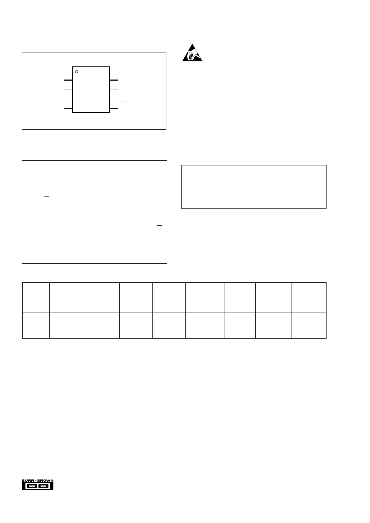
PIN NAME DESCRIPTION
1V
REF
Reference Input.
2 +In Non Inverting Input.
3 –In Inverting Input. Connect to ground or to remote
ground sense point.
4 GND Ground.
5 CS/SHDN Chip Select when LOW, Shutdown Mode when
HIGH.
6D
OUT
The serial output data word is comprised of 16
bits of data. In operation the data is valid on the
falling edge of DCLOCK. The
second clock pulse after the falling edge of CS
enables the serial output. After one null bit the
data is valid for the next 16 edges.
7 DCLOCK Data Clock synchronizes the serial data transfer
and determines conversion speed.
8+V
CC
Power Supply.
PIN ASSIGNMENTS
PIN CONFIGURATION
Top View MSOP
1
2
3
4
8
7
6
5
+V
CC
DCLOCK
D
OUT
CS/SHDN
V
REF
+In
–In
GND
ADS8320
PACKAGE/ORDERING INFORMATION
MAXIMUM NO
INTEGRAL MISSING
LINEARITY CODE PACKAGE SPECIFICATION
ERROR ERROR DRAWING TEMPERATURE PACKAGE ORDERING TRANSPORT
PRODUCT (%) (LSB) PACKAGE NUMBER
(1)
RANGE MARKING
(2)
NUMBER
(3)
MEDIA
ADS8320E 0.018 14 MSOP-8 337 –40°C to +85°C A20 ADS8320E/250 Tape and Reel
ADS8320E
""""""ADS8320E/2K5 Tape and Reel
ADS8320EB 0.012 15 MSOP-8 337 –40°C to +85°C A20 ADS8320EB/250 Tape and Reel
ADS8320EB
""""""ADS8320EB/2K5 Tape and Reel
NOTE: (1) For detail drawing and dimension table, please see end of data sheet or Package Drawing File on Web. (2) Performance Grade information is marked
on the reel. (3) Models with a slash(/) are available only in Tape and reel in quantities indicated (e.g. /250 indicates 250 units per reel, /2K5 indicates 2500 devices
per reel). Ordering 2500 pieces of ”ADS8320E/2K5“ will get a single 2500-piece Tape and Reel. For detailed Tape and Reel mechanical information, refer to the
www.burr-brown.com web site under Applications and Tape and Reel Orientation and Dimensions.
 Loading...