

Burr Brown Corporation ADS802, ADS802U, ADS802E-1K Datasheet
®
ADS802E
ADS802U
ADS802
12-Bit, 10MHz Sampling
ANALOG-TO-DIGITAL CONVERTER
FEATURES
● NO MISSING CODES
● LOW POWER: 250mW
● INTERNAL REFERENCE
● WIDEBAND TRACK/HOLD: 65MHz
● SINGLE +5V SUPPLY
APPLICATIONS
● IF AND BASEBAND DIGITIZATION
● DATA ACQUISITION CARDS
● TEST INSTRUMENTATION
● CCD IMAGING
Copiers
Scanners
Cameras
● VIDEO DIGITIZING
● GAMMA CAMERAS
TM
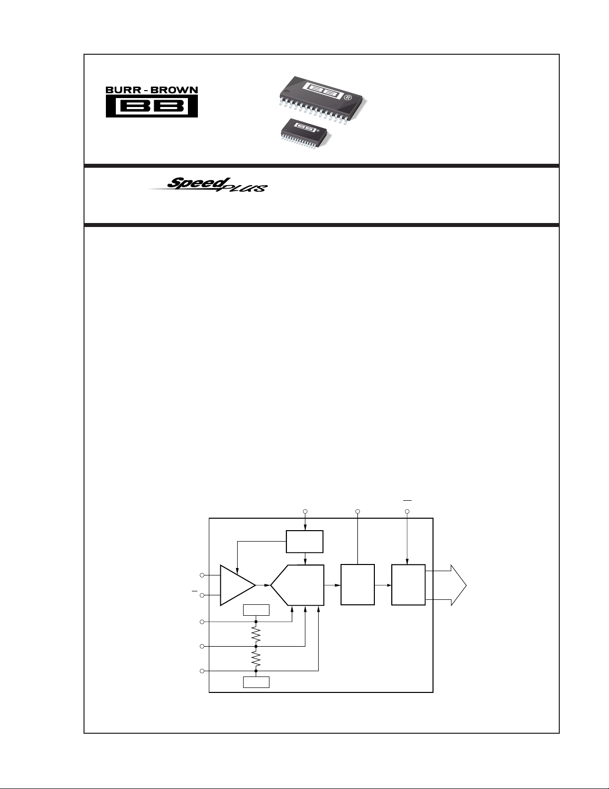
DESCRIPTION
The ADS802 is a low power, monolithic 12-bit, 10MHz
analog-to-digital converter utilizing a small geometry
CMOS process. This COMPLETE converter includes
a 12-bit quantizer, wideband track/hold, reference and
three-state outputs. It operates from a single +5V
power supply and can be configured to accept either
differential or single-ended input signals.
The ADS802 employs digital error correction in order
to provide excellent Nyquist differential linearity performance for demanding imaging applications. Its low
distortion, high SNR, and high oversampling capability
give it the extra margin needed for telecommunications,
test instrumentation and video applications.
This high performance A/D converter is specified for
AC and DC performance at a 10MHz sampling rate.
The ADS802 is available in 28-lead SOIC and SSOP
packages.
CLK
Timing
Circuitry
IN
IN
REFT
CM
REFB
International Airport Industrial Park • Mailing Address: PO Box 11400, Tucson, AZ 85734 • Street Address: 6730 S. Tucson Blvd., Tucson, AZ 85706 • Tel: (520) 746-1111 • Twx: 910-952-1111
Internet: http://www.burr-brown.com/ • FAXLine: (800) 548-6133 (US/Canada Only) • Cable: BBRCORP • Telex: 066-6491 • FAX: (520) 889-1510 • Immediate Product Info: (800) 548-6132
©
1995 Burr-Brown Corporation PDS-1290E Printed in U.S.A. October, 1996
T/H
+3.25V
+1.25V
Pipeline
A/D
MSBI OE
Error
Correction
Logic
3-State
Outputs
12-Bit
Digital
Data
SPECIFICATIONS
At TA = +25°C, VS = +5V, and Sampling Rate = 10MHz, with a 50% duty cycle clock having 2ns rise/fall time, unless otherwise noted.
ADS802U, E
PARAMETER CONDITIONS TEMP MIN TYP MAX UNITS
Resolution 12 Bits
Specified Temperature Range T
ANALOG INPUT
Differential Full Scale Input Range Both Inputs +1.25 +3.25 V
Common-Mode Voltage +2.25 V
Analog Input Bandwidth (–3dB)
Small Signal –20dBFS
Full Power 0dBFS Input +25°C 65 MHz
Input Impedance 1.25 || 4 MΩ || pF
DIGITAL INPUT
Logic Family TTL/HCT Compatible CMOS
Convert Command Start Conversion Falling Edge
ACCURACY
Gain Error +25°C ±0.6 ±1.5 %
Gain Tempco ±85 ppm/°C
Power Supply Rejection of Gain Delta +V
Input Offset Error Full ±2.1 ±3.0 %
Power Supply Rejection of Offset Delta +V
CONVERSION CHARACTERISTICS
Sample Rate 10k 10M Sample/s
Data Latency 6.5 Convert Cycle
DYNAMIC CHARACTERISTICS
Differential Linearity Error
f = 500kHz +25°C ±0.3 ±1.0 LSB
f = 5MHz +25°C ±0.4 ±1.0 LSB
No Missing Codes 0°C to +85°C Guaranteed LSB
Integral Linearity Error at f = 500kHz Best Fit 0°C to +85°C ±1.7 ±2.75 LSB
Spurious-Free Dynamic Range (SFDR)
f = 500kHz (–1dBFS input) +25°C 67 77 dBFS
f = 5MHz (–1dBFS input) +25°C 63 67 dBFS
Two-Tone Intermodulation Distortion (IMD)
f = 4.4MHz and 4.5MHz (–7dBFS each tone) +25°C –65 dBc
Signal-to-Noise Ratio (SNR)
f = 500kHz (–1dBFS input) +25°C65 67 dB
f = 5MHz (–1dBFS input) +25°C64 66 dB
Signal-to-(Noise + Distortion) (SINAD)
f = 500kHz (–1dBFS input) +25°C63 66 dB
f = 5MHz (–1dBFS input) +25°C61 63 dB
Differential Gain Error NTSC or PAL +25°C 0.5 %
Differential Phase Error NTSC or PAL +25°C 0.1 degrees
Aperture Delay Time +25°C2 ns
Aperture Jitter +25°C 7 ps rms
Overvoltage Recovery Time
NOTE: (1) dBFS refers to dB below Full Scale. (2). Percentage accuracies are referred to the internal A/D Full Scale Range of 4Vp-p. (3) IMD is referred to the
larger of the two input signals. If referred to the peak envelope signal (≈0dB), the intermodulation products will be 7dB lower. (4) No "rollover" of bits.
(2)
(3)
(4)
AMBIENT
(1)
Input +25°C 400 MHz
Full ±1.0 ±2.5 %
= ±5% +25°C 0.03 0.1 %FSR/%
S
= ±5% +25°C 0.05 0.1 %FSR/%
S
0°C to +85°C ±0.4 ±1.0 LSB
0°C to +85°C ±0.4 ±1.0 LSB
Full 66 75 dBFS
Full 62 66 dBFS
Full –64 dBc
Full 64 67 dB
Full 62 66 dB
Full 61 65 dB
Full 60 62 dB
1.5x Full Scale Input +25°C2 ns
–40 +85 °C
The information provided herein is believed to be reliable; however, BURR-BROWN assumes no responsibility for inaccuracies or omissions. BURR-BROWN assumes
no responsibility for the use of this information, and all use of such information shall be entirely at the user’s own risk. Prices and specifications are subject to change
without notice. No patent rights or licenses to any of the circuits described herein are implied or granted to any third party. BURR-BROWN does not authorize or warrant
any BURR-BROWN product for use in life support devices and/or systems.
®
ADS802
2

SPECIFICATIONS (CONT)
At TA = +25°C, VS = +5V, and Sampling Rate = 10MHz, with a 50% duty cycle clock having a 2ns rise/fall time, unless otherwise noted.
ADS802U, E
PARAMETER CONDITIONS TEMP MIN TYP MAX UNITS
OUTPUTS
Logic Family TTL/HCT Compatible CMOS
Logic Coding Logic Selectable SOB or BTC
Logic Levels Logic “LO” Full 0 0.4 V
3-State Enable Time Full 20 40 ns
3-State Disable Time Full 2 10 ns
POWER SUPPLY REQUIREMENTS
Supply Voltage: +V
Supply Current: +I
Power Consumption Operating +25°C 250 310 mW
Thermal Resistance,
28-Lead SOIC 75 °C/W
28-Lead SSOP 50 °C/W
S
S
θ
JA
Logic “HI” Full 2.0 +V
Operating Full +4.75 +5.0 +5.25 V
Operating +25°C5062mA
Operating Full 52 62 mA
Operating Full 260 310 mW
S
V
ABSOLUTE MAXIMUM RATINGS
+VS.......................................................................................................+6V
Analog Input.............................................................. 0V to (+V
Logic Input ................................................................ 0V to (+V
Case Temperature ......................................................................... +100°C
Junction Temperature .................................................................... +150°C
Storage Temperature..................................................................... +125°C
External Top Reference Voltage (REFT) .................................. +3.4V Max
External Bottom Reference Voltage (REFB).............................. +1.1V Min
NOTE: Stresses above these ratings may permanently damage the device.
+ 300mV)
S
+ 300mV)
S
PACKAGE/ORDERING INFORMATION
PACKAGE
DRAWING TEMPERATURE
PRODUCT PACKAGE NUMBER
ADS802U 28-Lead SOIC 217 –40°C to +85°C
ADS802E 28-Lead SSOP 324 –40°C to +85°C
NOTE: (1) For detailed drawing and dimension table, please see end of data
sheet, or Appendix C of Burr-Brown IC Data Book.
(1)
RANGE
ELECTROSTATIC
DISCHARGE SENSITIVITY
This integrated circuit can be damaged by ESD. Burr-Brown
recommends that all integrated circuits be handled with appropriate precautions. Failure to observe proper handling and
installation procedures can cause damage.
Electrostatic discharge can cause damage ranging from
performance degradation to complete device failure. BurrBrown Corporation recommends that all integrated circuits be
handled and stored using appropriate ESD protection
methods.
®
3
ADS802
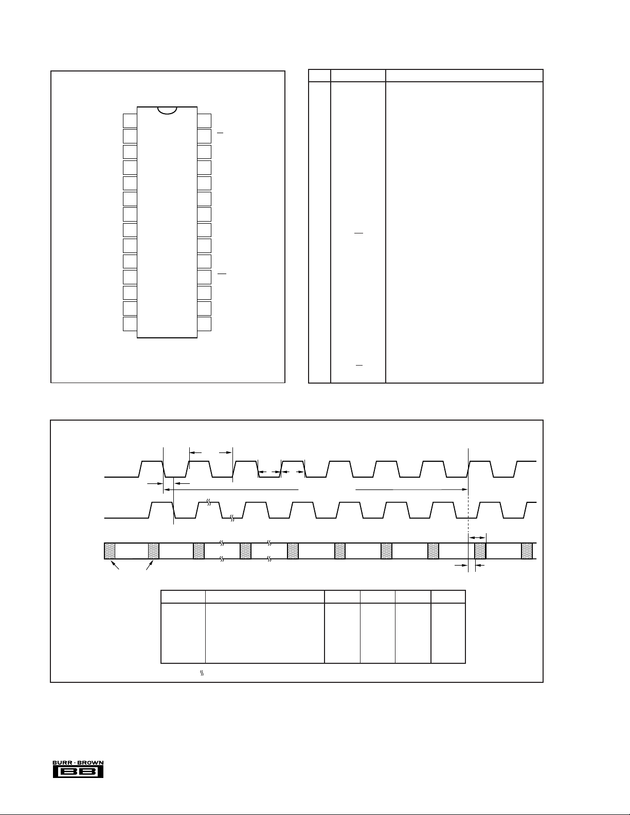
TOP VIEW SOIC/SSOP
GND
B10
B11
B12
GND
B1
B2
B3
B4
B5
B6
B7
B8
B9
1
2
3
4
5
6
7
ADS802
8
9
10
11
12
13
14
28
GND
27
IN
26
IN
25
GND
24
+V
S
23
REFT
22
CM
21
REFB
20
+V
S
19
MSBI
18
OE
17
+V
S
16
CLK
15
+V
S
PIN DESCRIPTIONSPIN CONFIGURATION
PIN DESIGNATOR DESCRIPTION
1 GND Ground
2 B1 Bit 1, Most Significant Bit
3 B2 Bit 2
4 B3 Bit 3
5 B4 Bit 4
6 B5 Bit 5
7 B6 Bit 6
8 B7 Bit 7
9 B8 Bit 8
10 B9 Bit 9
11 B10 Bit 10
12 B11 Bit 11
13 B12 Bit 12, Least Significant Bit
14 GND Ground
15 +V
16 CLK Convert Clock Input, 50% Duty Cycle
17 +V
18 OE HI: High Impedance State. LO or Floating: Nor-
19 MSBI Most Significant Bit Inversion, HI: MSB inverted
20 +V
21 REFB Bottom Reference Bypass. For external bypass-
22 CM Common-Mode Voltage. It is derived by
23 REFT Top Reference Bypass. For external bypassing
24 +V
25 GND Ground
26 IN Input
27 IN Complementary Input
28 GND Ground
+5V Power Supply
S
+5V Power Supply
S
mal Operation. Internal pull-down resistors.
for complementary output. LO or Floating: Straight
output. Internal pull-down resistors.
+5V Power Supply
S
ing of internal +1.25V reference.
(REFT + REFB)/2.
of internal +3.25V reference.
+5V Power Supply
S
TIMING DIAGRAM
CONVERT
CLOCK
INTERNAL
TRACK/HOLD
OUTPUT
DATA
Data Valid
N-8
Data Invalid
t
CONV
t
t
Track
Data Valid
D
Hold
N-7
(1)
Hold
Track Track Track Track
"N"
"N + 1"
Data Valid
N-6
LtH
Hold
"N + 2"
DATA LATENCY
(6.5 Clock Cycles)
Hold
Track
"N + 3"
Hold
"N + 4"
N-3N-5 N-4 N-2 N-1
Hold
Track Track
"N + 5
"
SYMBOL DESCRIPTION MIN TYP MAX UNITS
t
CONV
t
L
t
H
t
D
t
1
t
2
Convert Clock Period 100 100µsns
Clock Pulse Low 48 50 ns
Clock Pulse High 48 50 ns
Aperture Delay 2 ns
Data Hold Time, CL = 0pF 3.9 ns
New Data Delay Time, CL = 15pF max
12.5 ns
NOTE: (1) “ ” indicates the portion of the waveform that will stretch out at slower sample rates.
Hold
"N + 6"
t
1
t
2
N
®
ADS802
4
 Loading...