

Burr Brown Corporation ADS7845E-2K5, ADS7845 Datasheet
ADS7845
FEATURES
● 5-WIRE TOUCH SCREEN INTERFACE
● RATIOMETRIC CONVERSION
● SINGLE SUPPLY: 2V to 5V
● UP TO 125kHz CONVERSION RATE
● SERIAL INTERFACE
● PROGRAMMABLE 8- OR 12-BIT RESOLUTION
● AUXILIARY ANALOG INPUTS
● FULL POWER-DOWN CONTROL
®
DESCRIPTION
The ADS7845 is a 12-bit sampling analog-to-digital
converter (ADC) with a synchronous serial interface
and low on-resistance switches for driving touch
screens. Typical power dissipation is 750µW at a
125kHz throughput rate and a +2.7V supply. The
reference voltage (V
REF
) can be varied between 1V and
+VCC, providing a corresponding input voltage range
of 0V to V
REF
. The device includes a shutdown mode
which reduces typical power dissipation to under
0.5µW. The ADS7845 is guaranteed down to 2.7V
operation.
Low power, high speed, and on-board switches make
the ADS7845 ideal for battery-operated systems such
as personal digital assistants with resistive touch screens
and other portable equipment. The ADS7845 is available in a 16-lead SSOP package and is guaranteed
over the –40°C to +85°C temperature range.
APPLICATIONS
● PERSONAL DIGITAL ASSISTANTS
● PORTABLE INSTRUMENTS
● POINT-OF-SALES TERMINALS
● PAGERS
● TOUCH-SCREEN MONITORS
©
1998 Burr-Brown Corporation PDS-1497A Printed in U.S.A. December, 1998
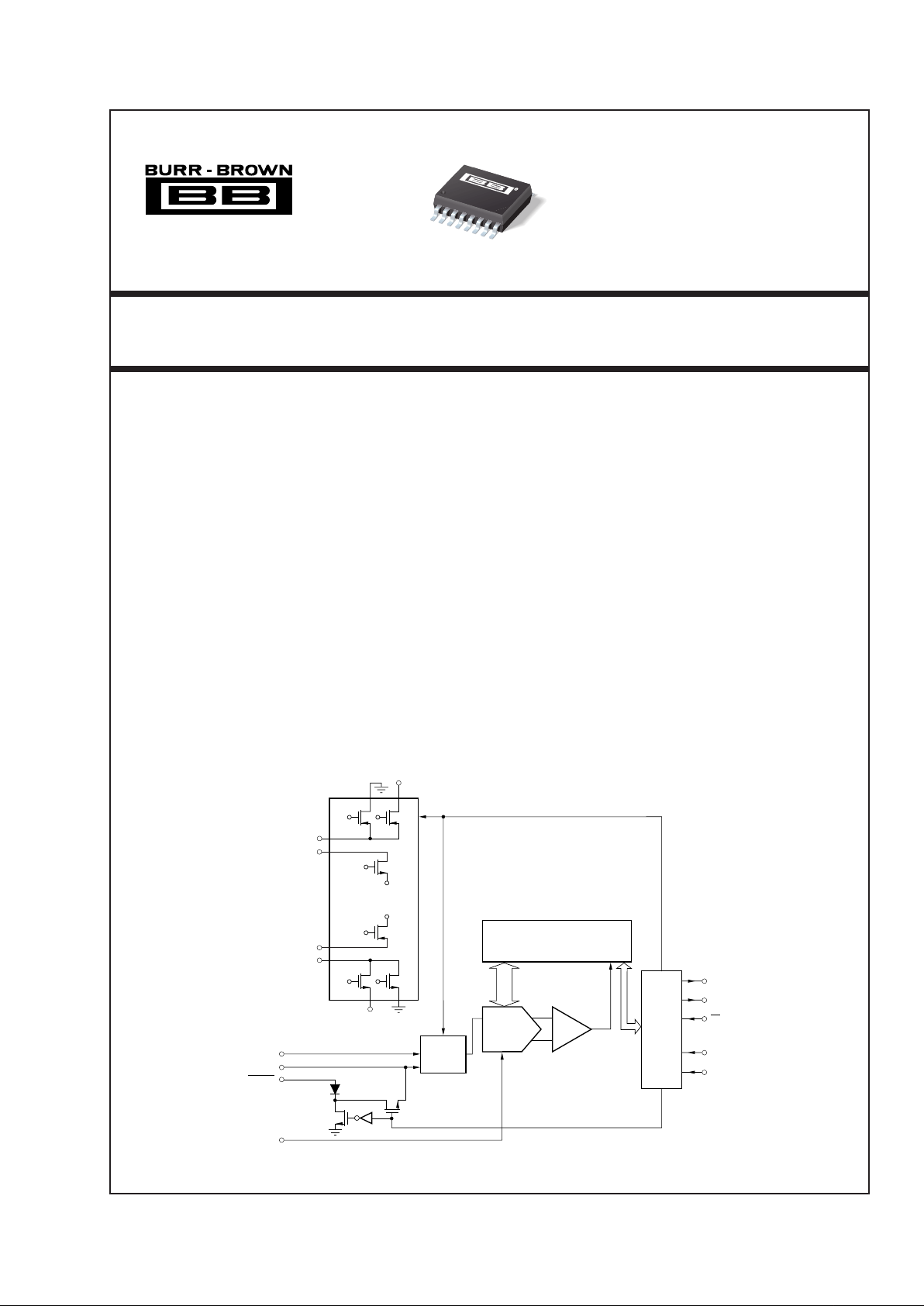
TOUCH SCREEN CONTROLLER
CDAC
SAR
ADS7845
Comparator
MUX
Serial
Data
Interface
and
Control
DOUT
BUSY
CS
DCLK
DIN
UR
LR
UL
LL
AUX IN
WIPER
PENIRQ
V
REF
GND
Driver
+V
CC
+V
CC
GND
+V
CC
GND
International Airport Industrial Park • Mailing Address: PO Box 11400, Tucson, AZ 85734 • Street Address: 6730 S. Tucson Blvd., Tucson, AZ 85706 • Tel: (520) 746-1111
Twx: 910-952-1111 • Internet: http://www.burr-brown.com/ • Cable: BBRCORP • Telex: 066-6491 • FAX: (520) 889-1510 • Immediate Product Info: (800) 548-6132
ADS7845
®
2
ADS7845
PARAMETER CONDITIONS MIN TYP MAX UNITS
RESOLUTION 12 Bits
ANALOG INPUT
Full-Scale Input Span Positive Input - Negative Input 0 V
REF
V
Absolute Input Range Positive Input –0.2 +V
CC
+0.2 V
Negative Input –0.2 +0.2 V
Capacitance 25 pF
Leakage Current 0.1 µA
SYSTEM PERFORMANCE
No Missing Codes 11 Bits
Integral Linearity Error ±2 LSB
(1)
Offset Error ±6 LSB
Gain Error ±4 LSB
Noise 30 µVrms
Power Supply Rejection Ratio 70 dB
SAMPLING DYNAMICS
Conversion Time 12 Clk Cycles
Acquisition Time 3 Clk Cycles
Throughput Rate 125 kHz
Multiplexer Settling Time 500 ns
Aperture Delay 30 ns
Aperture Jitter 100 ps
Channel-to-Channel Isolation V
IN
= 2.5Vp-p at 50kHz 100 dB
SWITCH DRIVERS
On-Resistance
UL, UR 7 Ω
LL, LR 7 Ω
REFERENCE INPUT
Range 1.0 +V
CC
V
Resistance CS = GND or +V
CC
5GΩ
Input Current 13 40 µA
f
SAMPLE
= 12.5kHz 2.5 µA
CS = +V
CC
0.001 3 µA
DIGITAL INPUT/OUTPUT
Logic Family CMOS
Logic Levels, Except PENIRQ
V
IH
| I
IH
| ≤ +5µA+V
CC
• 0.7 +VCC +0.3
V
IL
| I
IL
| ≤ +5µA –0.3 +0.8 V
V
OH
IOH = –250µA+V
CC
• 0.8 V
V
OL
IOL = 250µA 0.4 V
PENIRQ
V
OL
TA = 0°C to +85°C, 100kΩ Pull-Up 0.8 V
Data Format Straight Binary
POWER SUPPLY REQUIREMENTS
+V
CC
Specified Performance
(2)
2.7 5.5 V
Quiescent Current 280 650 µA
f
SAMPLE
= 12.5kHz 220 µA
Shutdown Mode with 3 µA
DCLK = DIN = +V
CC
Power Dissipation +VCC = +2.7V 1.8 mW
TEMPERATURE RANGE
Specified Performance –40 +85 °C
SPECIFICATIONS
At TA = –40°C to +85°C, +VCC = +2.7V, V
REF
= +2.5V, f
SAMPLE
= 125kHz, f
CLK
= 16 • f
SAMPLE
= 2MHz, 12-bit mode, and digital inputs = GND or +VCC, unless
otherwise noted.
The information provided herein is believed to be reliable; however, BURR-BROWN assumes no responsibility for inaccuracies or omissions. BURR-BROWN assumes
no responsibility for the use of this information, and all use of such information shall be entirely at the user’s own risk. Prices and specifications are subject to change
without notice. No patent rights or licenses to any of the circuits described herein are implied or granted to any third party. BURR-BROWN does not authorize or warrant
any BURR-BROWN product for use in life support devices and/or systems.
ADS7845E
NOTE: (1) LSB means Least Significant Bit. With V
REF
equal to +2.5V, one LSB is 610µV. (2) ADS7845 will operate down to 2.0V.

®
3
ADS7845
PIN NAME DESCRIPTION
1+V
CC
Power Supply, 2.0V to 5V.
2 UL Upper Left Panel Driver (V
CC
ON/OFF)
3 UR Upper Right Panel Driver (switch between V
CC
and GND)
4 LL Lower Left Panel Driver (switch between GND
and V
CC
)
5 LR Lower Right Panel Driver (GND ON/OFF)
6 GND Ground
7 WIPER Panel Input
8 AUXIN Auxiliary Input
9V
REF
Voltage Reference Input
10 +V
CC
Power Supply, 2.0V to 5V.
11 PENIRQ Pen Interrupt. Open anode output (requires 10kΩ
to 100kΩ pull-up resistor externally).
12 DOUT Serial Data Output. Data is shifted on the falling
edge of DCLK. This output is high impedance
when CS is HIGH.
13 BUSY Busy Output. This output is high impedance when
CS is HIGH.
14 DIN Serial Data Input. If CS is LOW, data is latched on
rising edge of DCLK.
15 CS Chip Select Input. Controls conversion timing and
enables the serial input/output register.
16 DCLK External Clock Input. This clock runs the SAR con-
version process and synchronizes serial data I/O.
PIN CONFIGURATION
Top View SSOP
PIN DESCRIPTION
ABSOLUTE MAXIMUM RATINGS
(1)
+V
CC
to GND ........................................................................ –0.3V to +6V
Analog Inputs to GND ............................................ –0.3V to +V
CC
+ 0.3V
Digital Inputs to GND .............................................–0.3V to +V
CC
+ 0.3V
Power Dissipation .......................................................................... 250mW
Maximum Junction Temperature................................................... +150°C
Operating Temperature Range ........................................–40°C to +85°C
Storage Temperature Range ......................................... –65°C to +150°C
Lead Temperature (soldering, 10s) ............................................... +300°C
NOTE: (1) Stresses above those listed under “Absolute Maximum Ratings”
may cause permanent damage to the device. Exposure to absolute maximum
conditions for extended periods may affect device reliability.
ELECTROSTATIC
DISCHARGE SENSITIVITY
This integrated circuit can be damaged by ESD. Burr-Brown
recommends that all integrated circuits be handled with
appropriate precautions. Failure to observe proper handling and
installation procedures can cause damage.
ESD damage can range from subtle performance degradation to
complete device failure. Precision integrated circuits may be
more susceptible to damage because very small parametric
changes could cause the device not to meet its published specifications.
MAXIMUM
INTEGRAL PACKAGE SPECIFICATION
LINEARITY DRAWING TEMPERATURE ORDERING TRANSPORT
PRODUCT ERROR (LSB) PACKAGE NUMBER
(1)
RANGE NUMBER
(2)
MEDIA
ADS7845E ±2 16-Lead SSOP 322 –40°C to +85°C ADS7845E Rails
"" """ADS7845E/2K5 Tape and Reel
NOTES: (1) For detailed drawing and dimension table, please see end of data sheet, or Appendix C of Burr-Brown IC Data Book. (2) Models with a slash (/) are
available only in Tape and Reel in the quantities indicated (e.g., /2K5 indicates 2500 devices per reel). Ordering 2500 pieces of “ADS7845E/2K5” will get a single
2500-piece Tape and Reel. For detailed Tape and Reel mechanical information, refer to Appendix B of Burr-Brown IC Data Book.
PACKAGE/ORDERING INFORMATION
1
2
3
4
5
6
7
8
+V
CC
UL
UR
LL
LR
GND
WIPER
AUXIN
DCLK
CS
DIN
BUSY
DOUT
PENIRQ
+V
CC
V
REF
16
15
14
13
12
11
10
9
ADS7845
®
4
ADS7845
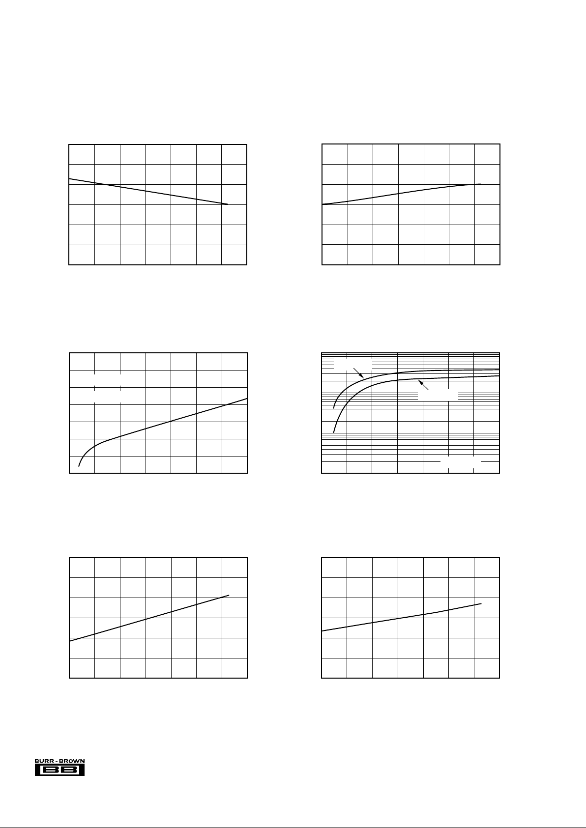
TYPICAL PERFORMANCE CURVES
At TA = +25°C, +VCC = +2.7V, V
REF
= +2.5V, f
SAMPLE
= 125kHz, and f
CLK
= 16 • f
SAMPLE
= 2MHz, unless otherwise noted.
SUPPLY CURRENT vs +V
CC
3.51.5 2 52.5 4
+V
CC
(V)
Supply Current (µA)
400
350
300
250
200
150
100
50
4.53
f
CLOCK
= 200kHz
V
REF
= +VCC
SUPPLY CURRENT vs TEMPERATURE
20–40 100–20 0 40
Temperature (°C)
Supply Current (µA)
400
350
300
250
200
150
100
60 80
POWER-DOWN SUPPLY CURRENT
vs TEMPERATURE
20–40 100–20 0 40
Temperature (°C)
Supply Current (nA)
140
120
100
80
60
40
20
60 80
MAXIMUM SAMPLE RATE vs +V
CC
3.51.5 2 52.5 4
+V
CC
(V)
Sample Rate (Hz)
1M
100k
10k
1k
4.53
V
REF
= +VCC
12-Bit Mode
8-Bit Mode
CHANGE IN GAIN vs TEMPERATURE
20–40 100–20 0 40
Temperature (°C)
Delta from +25°C (LSB)
0.15
0.10
0.05
0.00
–0.05
–0.10
–0.15
60 80
CHANGE IN OFFSET vs TEMPERATURE
20–40 100–20 0 40
Temperature (°C)
Delta from +25°C (LSB)
0.6
0.4
0.2
0.0
–0.2
–0.4
–0.6
60 80
 Loading...