Burr Brown Corporation ADS7832BP, ADS7832 Datasheet
®
ADS7832
ADS7832
ADS7832
Autocalibrating, 4-Channel, 12-Bit
ANALOG-TO-DIGITAL CONVERTER
FEATURES
● PIN COMPATIBLE TO ADC7802 AND
ADS7803
● SINGLE SUPPLY: +5V OR +3.3V
● LOW POWER: 14mW plus Power Down
● SIGNAL-TO-(NOISE + DISTORTION)
RATIO OVER TEMPERATURE:
69dB min with fIN = 1kHz
66dB min with fIN = 50kHz
● FAST CONVERSION TIME: 8.5µs
Including Acquisition (117kHz Sampling
Rate)
● FOUR-CHANNEL INPUT MULTIPLEXER
● AUTOCAL: No offset or Gain Adjust
Required
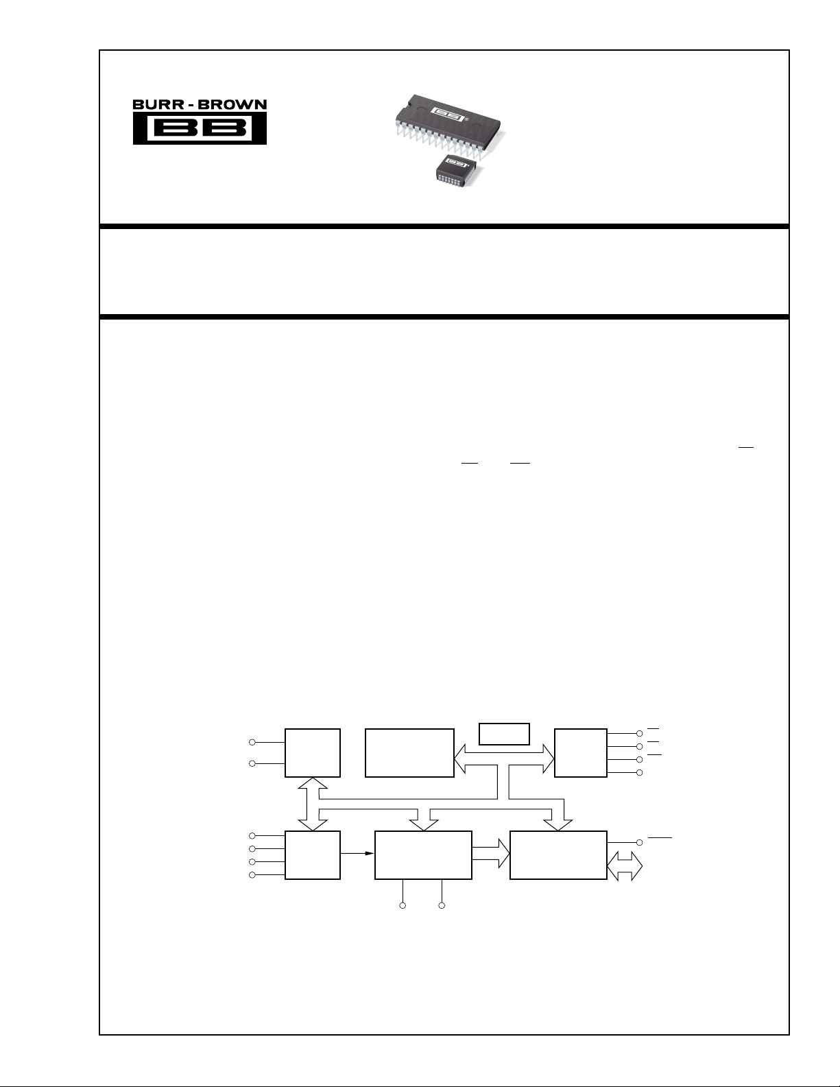
A0
A1
Address
Latch and
Decoder
Calibration
Microcontroller
and Memory
DESCRIPTION
The ADS7832 is a monolithic CMOS 12-bit analogto-digital converter with internal sample/hold and fourchannel multiplexer. It is designed and tested for full
dynamic performance with input signals to 50kHz.
The 5V single-supply requirements and standard CS,
RD, and WR control signals make the part easy to use
in microprocessor applications. Conversion results are
available in two bytes through an 8-bit three-state
output bus.
The ADS7832 is available in a 28-pin plastic DIP and
28-lead PLCC, fully specified for operation over the
industrial –40°C to +85°C temperature range.
Clock
Control
Logic
CS
RD
WR
SFR
AIN0
AIN1
AIN2
AIN3
International Airport Industrial Park • Mailing Address: PO Box 11400, Tucson, AZ 85734 • Street Address: 6730 S. Tucson Blvd., Tucson, AZ 85706 • Tel: (520) 746-1111 • Twx: 910-952-1111
Internet: http://www.burr-brown.com/ • FAXLine: (800) 548-6133 (US/Canada Only) • Cable: BBRCORP • Telex: 066-6491 • FAX: (520) 889-1510 • Immediate Product Info: (800) 548-6132
©
1996 Burr-Brown Corporation PDS-1332B Printed in U.S.A. April, 1998
Analog
Multiplexer
Capacitor Array
Sampling ADC
V
+V
REF
REF
Three-State
Input/Output
–
BUSY
8-Bit
Data Bus
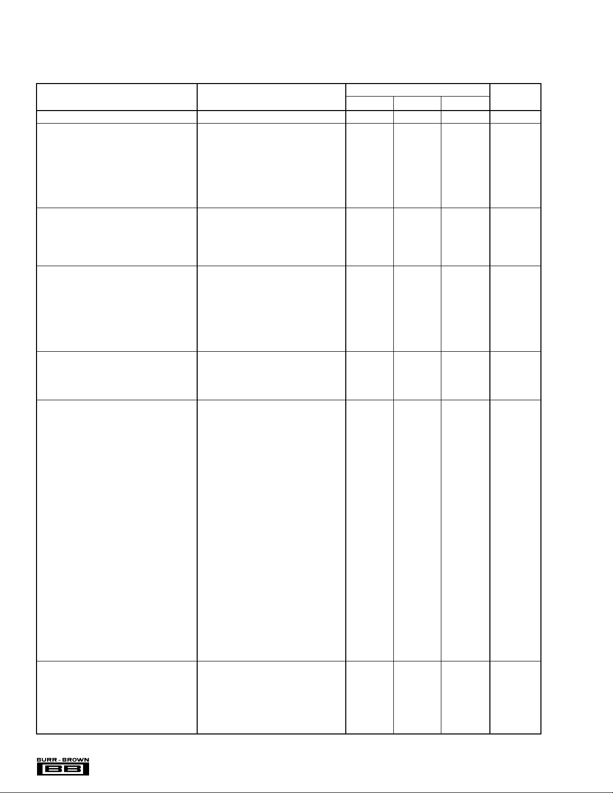
SPECIFICATIONS
ADS7832 Electrical Specifications with 3.3V Supply
VA = VD = V
PARAMETER CONDITIONS MIN TYP MAX UNITS
RESOLUTION 12 Bits
ANALOG INPUT V
Voltage Input Range 0V
Input Capacitance 40 pF
On State Bias Current 100 nA
Off State Bias Current T
On Resistance Multiplexer 400 Ω
Off Resistance Multiplexer 10 MΩ
Channel Separation F
REFERENCE INPUT
For Specified Performance: V
For Derated Performance
Input Reference Current 100 200 µA
THROUGHPUT SPEED
Conversion Time With External Clock (Including
Multiplexer Settling Time and Acquisition Time) CLK = 1MHz 17 µs
With Internal Clock Using Recommended T
Clock Components T
Slew Rate 2V/µs
Multiplexer Settling Time to 1/2 LSB 0.5 µs
Multiplexer Access Time 20 ns
SAMPLING DYNAMICS
Full Power Bandwidth –3dB 2 MHz
Aperture Jitter ps
Aperture Delay SRF D2 LOW
DC ACCURACY
Integral Nonlinearity, All Channels SFR D2 LOW ±0.75 LSB
Differential Nonlinearity ±0.75 LSB
No Missing Codes Guaranteed
Gain Error All Channels ±0.5 LSB
Gain Error Drift Between Calibration Cycles ±0.2 ppm/°C
Offset Error All Channels
Offset Error Drift Between Calibration Cycles
Channel-to-Channel Mismatch SFR D2 LOW ±0.25 LSB
Power Supply Sensitivity V
AC ACCURACY
Signal-to-(Noise + Distortion) Ratio f
Total Harmonic Distortion f
Signal-to-Noise Ratio f
Spurious Free Dynamic Range f
+ = 3.3V ±10%; V
REF
– = AGND = DGND = 0V; CLK = 1MHz external, TA = –40°C to +85°C, after calibration at any temperature, unless otherwise specified.
REF
ADS7832BP/ADS7832BN
= VD = V
A
T
= –40°C to +85°C 100 nA
A
= 1kHz, V
IN
+ V
REF
V
– 0V
REF
(2)
: V
+(V
REF
V
– 0 0.5 V
REF
REF
+) – (V
= 3.0V
REF+
= +25°C10nA
A
+ = 3.0V 0.5 LSB
REF
A
–) ≥ 2.5V 2.5 V
REF
REF+
A
V
V
V
CLK = 500kHz 34 µs
= +25°C30µs
A
= –40°C to +85°C30µs
A
(3)
5 µs
SFR D2 HIGH 5 ns
(4)
SFR D2 HIGH, Internal Clock or Sampling ±0.5 LSB
Command Synchronous to External Clock
SFR D2 HIGH, Sampling ±0.6 LSB
Command Asynchronous to External Clock
SFR D2 LOW ±0.75 LSB
SFR D2 HIGH, Internal Clock or Sampling ±1 LSB
Command Synchronous to External Clock
SFR D2 HIGH, Sampling ±4 LSB
Command Asynchronous to External Clock
SFR D2 LOW ±0.2 ppm/°C
SFR D2 HIGH, Internal Clock or Sampling ±0.5 ppm/°C
Command Synchronous to External Clock
SFR D2 HIGH, Sampling ±1 ppm/°C
Command Asynchronous to External Clock
SFR D2 HIGH, Internal Clock or Sampling ±0.5 LSB
Command Synchronous to External Clock
SFR D2 HIGH, Sampling ±1 LSB
Command Asynchronous to External Clock
= VA = +3.3V ±10% (without recalibration) ±0.125 LSB
D
= 1kHz 69 71 dB
IN
fIN = 50kHz 66 69 dB
= 50kHz –75 dB
IN
= 50kHz 70 dB
IN
= 1kHz 85 dB
IN
f
= 50kHz 82 dB
IN
(1)
®
ADS7832
2
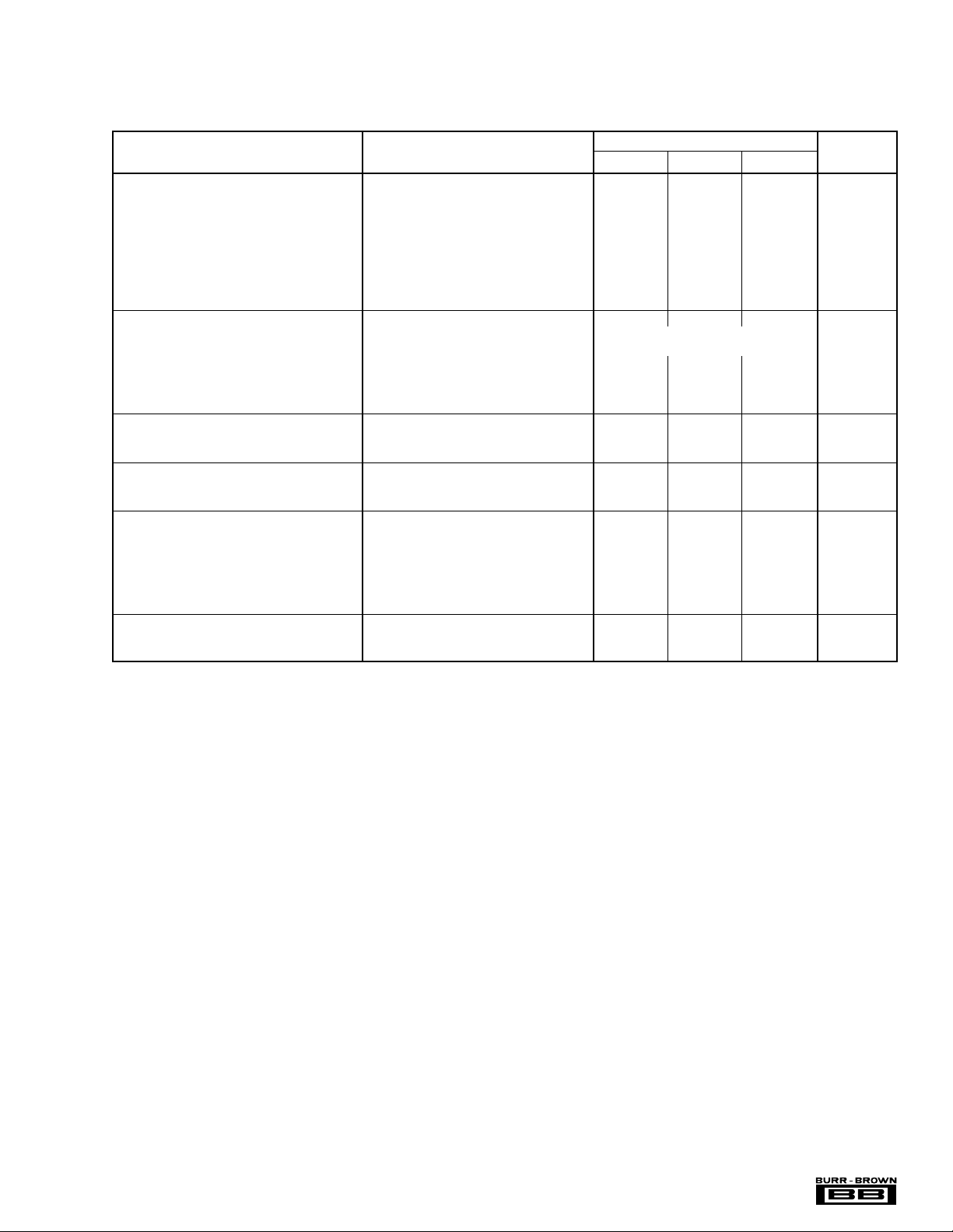
SPECIFICATIONS (CONT)
ADS7832 Electrical Specifications with 3.3V Supply
VA = VD = V
PARAMETER CONDITIONS MIN TYP MAX UNITS
DIGITAL INPUTS
Voltage Levels: V
Current Levels: I
DIGITAL OUTPUTS
Data Format Parallel 12 Bits in Two Bytes
Data Coding Straight Binary
V
V
Leakage Current High-Z State, V
Output Capacitance High-Z State 4 pF
CALIBRATION TIMING
Calibration Cycle Power On or Power Failure 37393 Clock Cycles
Calibration Cycle During Normal Operation 4625 Clock Cycles
DIGITAL TIMING
Bus Access Time 83 ns
Bus Relinquish Time 83 ns
POWER SUPPLIES
Supply Voltage for Specified Performance: V
Supply Current: I
Power Dissipation Power Up Mode or During Conversion 7.5 mW
TEMPERATURE RANGE
Specification –40 +85 °C
Storage –65 +150 °C
✻ These specifications need to be added based on performance of final silicon.
NOTES: (1) All specifications in dB are referred to a full-scale input range. (2) Over this range, total error will typically not exceed ±1LSB. (3) In this mode, the ADS7832
acquires the input signal for five clock cycles after a start command, before the input is held and conversion begins. (4) LSB means Least Significant Bit. For a 0V to
5V input range, one LSB is 1.22mV. For a 0V to 2.5V input range, one LSB is 610µV.
OL
OH
+ = 3.3V ±10%; V
REF
IL
V
IH
IL
I
IL
I
IH
I
IH
I
IH
I
IH
A
I
D
– = AGND = DGND = 0V; CLK = 1MHz external, TA = –40°C to +85°C, after calibration at any temperature, unless otherwise specified.
REF
ADS7832BP/ADS7832BN
–0.3 +0.8 V
0.7 • V
CAL (Internal Pull-Up) 10 µA
D
VD +0.3V V
All Other Inputs ±10 µA
SFR (Internal Pull-Down) 90 µA
CLK 1.5 mA
All Other Inputs ±10 µA
Power Down Mode (SFR D3 HIGH) ±100 nA
I
= 1.6mA 0.2 • V
SINK
I
= 200µA 0.8 • V
SOURCE
A
V
D
Tested at 3.0V 3 3.3 V
Tested at 3.0V 3 3.3 V
= 0V to V
OUT
D
D
2.5 3 mA
D
±1 µA
V
V
300 500 µA
Power Down Mode, No Clock Running 50 µW
The information provided herein is believed to be reliable; however, BURR-BROWN assumes no responsibility for inaccuracies or omissions. BURR-BROWN
assumes no responsibility for the use of this information, and all use of such information shall be entirely at the user’s own risk. Prices and specifications are subject
to change without notice. No patent rights or licenses to any of the circuits described herein are implied or granted to any third party. BURR-BROWN does not
authorize or warrant any BURR-BROWN product for use in life support devices and/or systems.
3
ADS7832
®
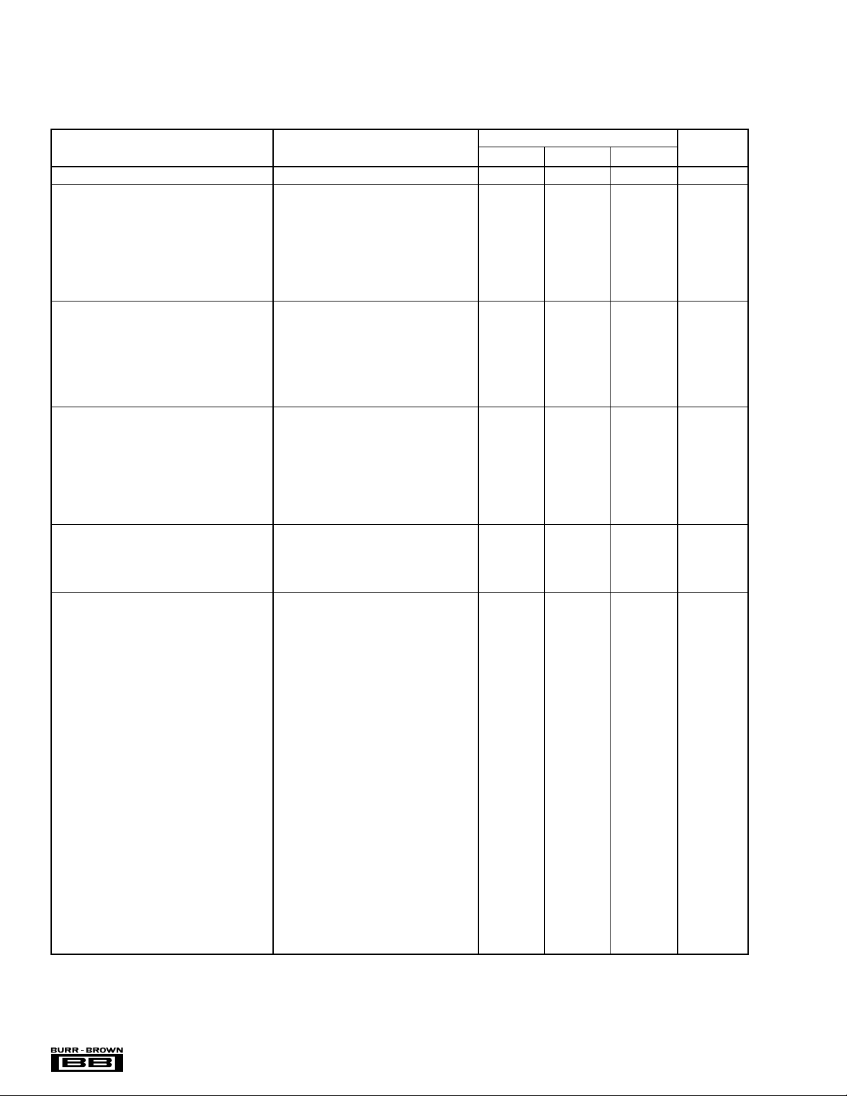
SPECIFICATIONS
ADS7832 Electrical Specifications with 5V Supply
VA = VD = 5V ±10%; V
unless otherwise specified.
PARAMETER CONDITIONS MIN TYP MAX UNITS
RESOLUTION 12 Bits
ANALOG INPUT
Voltage Input Range V
Input Capacitance 40 pF
On State Bias Current 100 nA
Off State Bias Current T
On Resistance Multiplexer 400 Ω
Off Resistance Multiplexer 10 MΩ
Channel Separation F
REFERENCE INPUT
For Specified Performance: V
V
+ V
REF
V
– 0V
REF
For Derated Performance
V
+ 2.5 V
REF
V
– 01V
REF
Input Reference Current 100 200 µA
THROUGHPUT SPEED
Conversion Time With External Clock (Including CLK = 2MHz 8.5 µs
Multiplexer Settling Time and Acquisition Time) CLK = 1MHz 17 µs
With Internal Clock Using Recommended T
Clock Components T
Slew Rate 2 mV/µs
Multiplexer Settling Time to 1/2 LSB 0.5 µs
Multiplexer Access Time 20 ns
SAMPLING DYNAMICS
Full Power Bandwidth –3dB 4 MHz
Aperture Jitter 10 ps
Aperture Delay SRF D2 LOW
DC ACCURACY
Integral Nonlinearity, All Channels SFR D2 LOW ±0.75 LSB
Differential Nonlinearity ±0.75 LSB
No Missing Codes Guaranteed
Gain Error All Channels ±0.50 LSB
Gain Error Drift Between Calibration Cycles ±0.2 ppm/°C
Offset Error All Channels
Offset Error Drift Between Calibration Cycles
Channel-to-Channel Mismatch SFR D2 LOW ±0.25 LSB
Power Supply Sensitivity V
+ = 5.0V; V
REF
(2)
– = AGND = DGND = 0V; CLK = 1MHz external 50% ±2% Duty Cycle, TA = –40°C to +85°C, after calibration at any temperature,
REF
= VA = V
D
T
A
= 1kHz, VD = VA = V
IN
:(V
REF
REF
= +25°C10nA
A
= –40°C to +85°C 100 nA
= VA = 5V
REF
+) – (V
–) ≥ 2.5V
REF
CLK = 500kHz 34 µs
= +25°C30µs
A
= –40°C to +85°C30µs
A
SFR D2 HIGH 5 ns
SFR D2 HIGH, Internal Clock or Sampling ±0.5 LSB
Command Synchronous to External Clock
SFR D2 HIGH, Sampling ±0.6 LSB
Command Asynchronous to External Clock
SFR D2 LOW ±0.75 LSB
SFR D2 HIGH, Internal Clock or Sampling ±1 LSB
Command Synchronous to External Clock
SFR D2 HIGH, Sampling ±4 LSB
Command Asynchronous to External Clock
SFR D2 LOW ±0.2 ppm/°C
SFR D2 HIGH, Internal Clock or Sampling ±0.5 ppm/°C
Command Synchronous to External Clock
SFR D2 HIGH, Sampling ±1 ppm/°C
Command Asynchronous to External Clock
SFR D2 HIGH, Internal Clock or Sampling ±0.5 LSB
Command Synchronous to External Clock
SFR D2 HIGH, Sampling ±1.0 LSB
Command Asynchronous to External Clock
= VA = +5V ±10% (without recalibration) ±0.125 LSB
D
ADS7832BP/ADS7832BN
+ = 5V 0 5 V
+ = 5V 0.5 LSB
REF
A
A
(3)
2.5 µs
V
V
(4)
®
ADS7832
4
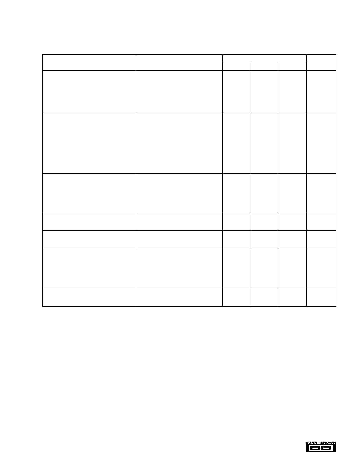
SPECIFICATIONS (CONT)
ADS7832 Electrical Specifications with 5V Supply
VA = VD = 5V ±10%; V
otherwise specified.
PARAMETER CONDITIONS MIN TYP MAX UNITS
AC ACCURACY
Signal-to-(Noise + Distortion) Ratio f
Total Harmonic Distortion f
Signal-to-Noise Ratio f
Spurious Free Dynamic Range f
DIGITAL INPUTS
Voltage Levels: V
Current Levels: I
DIGITAL OUTPUTS
Data Format Parallel 12 Bits in Two Bytes
Data Coding Straight Binary
V
OL
V
OH
Leakage Current High-Z State ±1 µA
Output Capacitance High-Z State 4 pF
CALIBRATION TIMING
Calibration Cycle Power On or Power Failure 37393 Clock Cycles
Calibration Cycle During Normal Operation 4625 Clock Cycles
DIGITAL TIMING
Bus Access Time 83 ns
Bus Relinquish Time 83 ns
POWER SUPPLIES
Supply Voltage for Specified Performance: V
Supply Current: I
Power Dissipation Power Up Mode or During Conversion 14 mW
TEMPERATURE RANGE
Specification –40 85 °C
Storage –65 150 °C
V
V
V
IL
I
IL
I
IH
I
IH
I
IH
I
IH
I
IL
IH
IL
IH
A
D
+ = 5V; V
REF
– = AGND = DGND = 0V; CLK = 1MHz external 50% ±2% Duty Cycle, TA = –40°C to +85°C, after calibration at any temperature, unless
REF
ADS7832BP/ADS7832BN
= 1kHz 69 71 dB
IN
fIN = 50kHz 66 69 dB
= 50kHz –75 dB
IN
= 50kHz 70 dB
IN
= 1kHz 85 dB
IN
f
= 50kHz 82 dB
IN
CLK –0.3 0.8 V
CLK 3.5 VD +0.3V V
All Others –0.3 0.8 V
All Others 2.4 VD +0.3V V
CAL (Internal Pull-Up) 10 µA
All Other Inputs ±10 µA
SFR (Internal Pull-Down) 90 µA
CLK 1.5 mA
All Other Inputs ±10 µA
Power Down Mode (SFR D3 HIGH) ±100 nA
I
= 1.6mA 0.4 V
SINK
I
= 200µA4 V
SOURCE
A
V
D
Tested at 5.5V 5 5.5 V
Tested at 5.5V 5 5.5 V
Tested at 5.5V 2.5 5.5 mA
Tested at 5.5V 300 500 µA
Power Down Mode, No Clock Running 50 µW
(1)
✻These specifications need to be added based on performance of final silicon.
NOTES: (1) All specifications in dB are referred to a full-scale input range. (2) Over this range, total error will typically not exceed ±1LSB. (3) In this mode, the ADS7832
acquires the input signal for five clock cycles after a start command, before the input is held and conversion begins. (4) LSB means Least Significant Bit. For a 0V to
5V input range, one LSB is 1.22mV. For a 0V to 2.5V input range, one LSB is 610µV.
5
ADS7832
®
 Loading...