

Burr Brown Corporation ADS7810UB-1K, ADS7810UB, ADS7810U-1K, ADS7810U Datasheet
12-Bit 800kHz Sampling CMOS
ANALOG-to-DIGITAL CONVERTER
FEATURES
● 1.25µs THROUGHPUT TIME
● STANDARD
±10V INPUT RANGE
● 69dB min SINAD WITH 250kHz INPUT
●
±3/4 LSB max INL AND ±1 LSB max DNL
● INTERNAL REFERENCE
● COMPLETE WITH S/H, REF, CLOCK, ETC.
● PARALLEL DATA w/LATCHES
● 28-PIN SOIC
ADS7810
DESCRIPTION
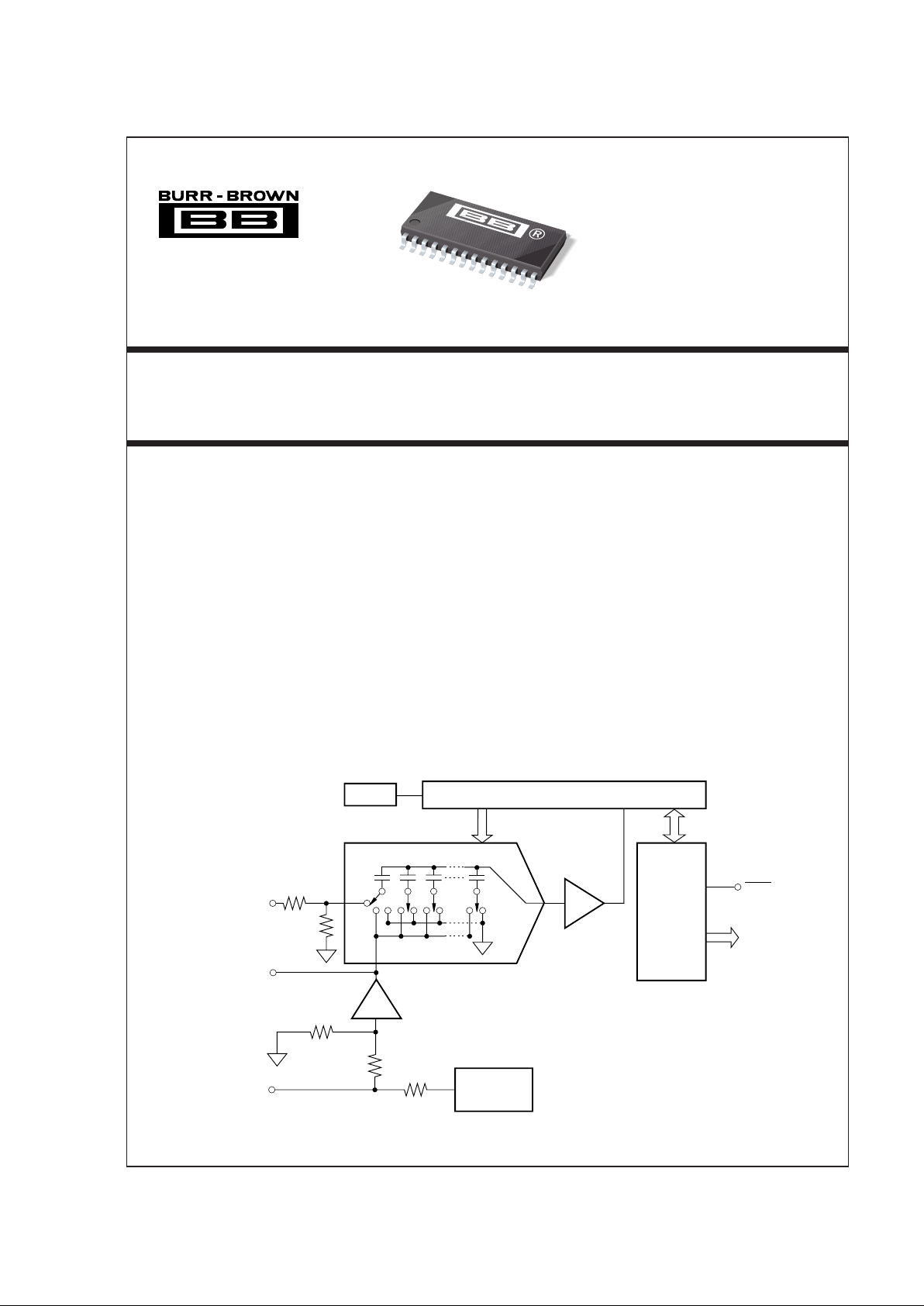
The ADS7810 is a complete 12-bit sampling A/D
using state-of-the-art CMOS structures. It contains a
complete 12-bit capacitor-based SAR A/D with inherent S/H, reference, clock, interface for microprocessor
use, and three-state output drivers.
The ADS7810 is specified at an 800kHz sampling
rate, and guaranteed over the full temperature range.
Laser-trimmed scaling resistors provide the industrystandard ±10V input range, while an innovative design
allows operation from ±5V supplies.
The 28-pin ADS7810 is available in a plastic SOIC
fully specified for operation over the industrial –40°C
to +85°C range.
®
© 1992 Burr-Brown Corporation PDS-1138E Printed in U.S.A. March, 1998
CDAC
Internal
Ref
Output
Latches
and
Three
State
Drivers
Three
State
Parallel
Data
Bus
BUSY
±10V Input
2.5V Ref Out/In
Comparator
Buffer
625Ω
2450Ω
Successive Approximation Register and Control Logic
Clock
Cap
4.8kΩ
8.6kΩ
18kΩ
International Airport Industrial Park • Mailing Address: PO Box 11400, Tucson, AZ 85734 • Street Address: 6730 S. Tucson Blvd., Tucson, AZ 85706 • Tel: (520) 746-1111 • Twx: 910-952-1111
Internet: http://www.burr-brown.com/ • FAXLine: (800) 548-6133 (US/Canada Only) • Cable: BBRCORP • Telex: 066-6491 • FAX: (520) 889-1510 • Immediate Product Info: (800) 548-6132
ADS7810
®
ADS7810 2
SPECIFICATIONS
ELECTRICAL
At TA = –40°C to +85°C, fS = 800kHz, +V
DIG
= +V
ANA
= +5V, –V
ANA
= –5V, using internal reference and the 50Ω input resistor shown in Figure 4b, unless otherwise specified.
The information provided herein is believed to be reliable; however, BURR-BROWN assumes no responsibility for inaccuracies or omissions. BURR-BROWN assumes
no responsibility for the use of this information, and all use of such information shall be entirely at the user’s own risk. Prices and specifications are subject to change
without notice. No patent rights or licenses to any of the circuits described herein are implied or granted to any third party. BURR-BROWN does not authorize or warrant
any BURR-BROWN product for use in life support devices and/or systems.
ADS7810U ADS7810UB
PARAMETER CONDITIONS MIN TYP MAX MIN TYP MAX UNITS
RESOLUTION 12 ✻ Bits
ANALOG INPUT
Voltage Range ±10 ✻ V
Impedance 3.1 ✻ kΩ
Capacitance 5 ✻ pF
THROUGHPUT SPEED
Conversion Cycle t
3
+ t
4
1020 ✻ ns
Complete Cycle Acquire & Convert 1250 ✻ ns
Throughput Rate 800 ✻ kHz
DC ACCURACY
Integral Linearity Error ±1 ±0.75 LSB
(1)
Differential Linearity Error ±1 ✻ LSB
No Missing Codes Guaranteed ✻
Transition Noise
(2)
0.1 ✻ LSB
Full Scale Error
(3, 4)
±0.5 ±0.25 %
Full Scale Error Drift ±12 ✻ ppm/°C
Full Scale Error
(3, 4)
Ext. 2.5000V Ref ±0.5 ✻ %
Full Scale Error Drift Ext. 2.5000V Ref ±12 ✻ ppm/°C
Bipolar Zero Error
(3)
±8 ±4 LSB
Bipolar Zero Error Drift ±2 ✻ ppm/°C
Power Supply Sensitivity
(+V
DIG
= +V
ANA
= VD) +4.75V < VD < +5.25V ±5 ✻ LSB
–5.25V < –V
ANA
< –4.75V ±0.5 ✻ LSB
AC ACCURACY
Spurious-Free Dynamic Range f
IN
= 250kHz 74 82 77 84 dB
(5)
Total Harmonic Distortion f
IN
= 250kHz –80 –74 –82 –77 dB
Signal-to-(Noise+Distortion) f
IN
= 250kHz 67 71 69 ✻ dB
Signal-to-Noise f
IN
= 250kHz 68 71 70 ✻ dB
Usable Bandwidth
(6)
1.5 ✻ MHz
SAMPLING DYNAMICS
Aperture Delay 20 ✻ ns
Aperture Jitter 10 ✻ ps
Transient Response FS Step 200 ✻ ns
Overvoltage Recovery
(7)
250 ✻ ns
REFERENCE
Internal Reference Voltage 2.48 2.5 2.52 ✻✻✻ V
Internal Reference DC Source Current 100 ✻ µA
(External load should be static)
Internal Reference Drift 8 ppm/°C
External Reference Voltage Range 2.3 2.5 2.7 ✻✻✻ V
For Specified Linearity
External Reference Current Drain Ext. 2.5000V Ref 100 ✻ µA
DIGITAL INPUTS
Logic Levels
V
IL
–0.3 +0.8 ✻✻V
V
IH
+2.4 VD + 0.3 ✻✻V
I
IL
VIL = 0V ±10 ✻ µA
I
IH
VIH = 5V ±10 ✻ µA
DIGITAL OUTPUTS
Data Format Parallel 12 Bits
Data Coding Binary Two’s Complement
V
OL
I
SINK
= 1.6mA +0.4 ✻ V
V
OH
I
SOURCE
= 500µA +2.8 ✻ V
Leakage Current High-Z State, ±5 ✻ µA
V
OUT
= 0V to V
DIG
Output Capacitance High-Z State 15 15 pF
DIGITAL TIMING
Bus Access Time 62 ✻ ns
Bus Relinquish Time 83 ✻ ns
®
ADS7810
3
ADS7810U ADS7810UB
PARAMETER CONDITIONS MIN TYP MAX MIN TYP MAX UNITS
POWER SUPPLIES
Specified Performance
+V
DIG
= +V
ANA
+4.75 +5 +5.25 ✻✻✻ V
–V
ANA
–5.25 –5 –4.75 ✻✻✻ V
+I
DIG
+16 ✻ mA
+I
ANA
+16 ✻ mA
–I
ANA
–13 ✻ mA
Derated Performance
+V
DIG
= +V
ANA
+4.5 +5 +5.5 ✻✻✻ V
–V
ANA
–5.5 –5 –4.5 ✻✻✻ V
Power Dissipation f
S
= 800kHz 225 275 ✻ mW
TEMPERATURE RANGE
Specified Performance –40 +85 ✻✻°C
Derated Performance –55 +125 °C
Storage –65 +150 ✻✻°C
Thermal Resistance (
θ
JA
)
Plastic DIP 75 ✻ °C/W
SOIC 75 ✻ °C/W
✻ Specification same as ADS7810U.
NOTES: (1) LSB means Least Significant Bit. For the 12-bit, ±10V input ADS7810, one LSB is 4.88mV. (2) Typical rms noise at worst case transitions and
temperatures. (3) Measured with 50Ω in series with analog input. Adjustable to zero with external potentiometer. (4) Full scale error is the worst case of –Full Scale
or +Full Scale untrimmed deviation from ideal first and last code transitions, divided by the transition voltage (not divided by the full-scale range) and includes the
effect of offset error. (5) All specifications in dB are referred to a full-scale ±10V input. (6) Usable Bandwidth defined as Full-Scale input frequency at which Signalto-(Noise+Distortion) degrades to 60dB, or 10 bits of accuracy. (7) Recovers to specified performance after 2 x FS input over voltage.
SPECIFICATIONS (CONT)
ELECTRICAL
At TA = –40°C to +85°C, fS = 800kHz, +V
DIG
= +V
ANA
= +5V, –V
ANA
= –5V, using internal reference and the 50Ω input resistor shown in Figure 4b, unless otherwise specified.
ABSOLUTE MAXIMUM RATINGS
Analog Inputs: VIN.............................................................................. ±25V
REF .................................... +V
ANA
+0.3V to AGND2 –0.3V
CAP ...........................................Indefinite Short to AGND2
Momentary Short to +V
ANA
Ground Voltage Differences: DGND, AGND1, AGND2 ...................±0.3V
+V
ANA
...................................................................................................+7V
+V
DIG
to +V
ANA
.................................................................................+0.3V
+V
DIG
..................................................................................................... 7V
–V
ANA
................................................................................................... –7V
Digital Inputs ............................................................ –0.3V to +V
DIG
+0.3V
Maximum Junction Temperature ................................................... +165°C
Internal Power Dissipation .............................................................825mW
Lead Temperature (soldering, 10s)................................................ +300°C
MINIMUM
MAXIMUM SIGNAL-TOINTEGRAL (NOISE + SPECIFICATION
LINEARITY DISTORTION) TEMPERATURE PACKAGE DRAWING
PRODUCT ERROR (LSB) RATIO (dB) RANGE PACKAGE NUMBER
(1)
ADS7810U ±1 67 –40°C to +85°C 28-Pin SOIC 217
ADS7810UB ±0.75 69 –40°C to +85°C 28-Pin SOIC 217
NOTE: (1) For detailed drawing and dimension table, please see end of data sheet, or Appendix C of Burr-Brown IC Data Book.
ORDERING/ PACKAGE INFORMATION
ELECTROSTATIC
DISCHARGE SENSITIVITY
This integrated circuit can be damaged by ESD. Burr-Brown
recommends that all integrated circuits be handled with
appropriate precautions. Failure to observe proper handling
and installation procedures can cause damage.
ESD damage can range from subtle performance degradation
to complete device failure. Precision integrated circuits may
be more susceptible to damage because very small parametric
changes could cause the device not to meet its published
specifications.
®
ADS7810 4
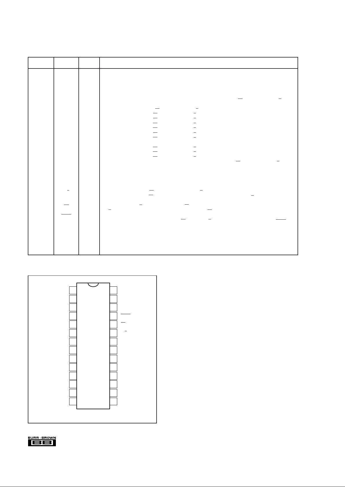
PIN ASSIGNMENTS
DIGITAL
PIN # NAME I/O DESCRIPTION
1V
IN
Analog Input. Connect via 50Ω to analog input. Full-scale input range is ±10V.
2 AGND1 Analog Ground. Used internally as ground reference point. Minimal current flow.
3 REF Reference Input/Output. Outputs internal reference of +2.5V nominal. Can also be driven by external system
reference. In both cases, decouple to ground with a 0.1µF ceramic capacitor.
4 CAP Reference Buffer Output. 10 µF tantalum capacitor to ground. Nominally +2V.
5 AGND2 Analog Ground.
6 D11 (MSB) O Data Bit 11. Most Significant Bit (MSB) of conversion results. Hi-Z state when CS is HIGH, or when R/C is
LOW, or when a conversion is in progress.
7 D10 O Data Bit 10. Hi-Z state when CS is HIGH, or when R/C is LOW, or when a conversion is in progress.
8 D9 O Data Bit 9. Hi-Z state when CS is HIGH, or when R/C is LOW, or when a conversion is in progress.
9 D8 O Data Bit 8. Hi-Z state when CS is HIGH, or when R/C is LOW, or when a conversion is in progress.
10 D7 O Data Bit 7. Hi-Z state when CS is HIGH, or when R/C is LOW, or when a conversion is in progress.
11 D6 O Data Bit 6. Hi-Z state when CS is HIGH, or when R/C is LOW, or when a conversion is in progress.
12 D5 O Data Bit 5. Hi-Z state when CS is HIGH, or when R/C is LOW, or when a conversion is in progress.
13 D4 O Data Bit 4. Hi-Z state when CS is HIGH, or when R/C is LOW, or when a conversion is in progress.
14 DGND Digital Ground.
15 D3 O Data Bit 3. Hi-Z state when CS is HIGH, or when R/C is LOW, or when a conversion is in progress.
16 D2 O Data Bit 2. Hi-Z state when CS is HIGH, or when R/C is LOW, or when a conversion is in progress.
17 D1 O Data Bit 1. Hi-Z state when CS is HIGH, or when R/C is LOW, or when a conversion is in progress.
18 D0 (LSB) O Data Bit 0. Least Significant Bit (LSB) of conversion results. Hi-Z state when CS is HIGH, or when R/C is
LOW, or when a conversion is in progress.
19 Not internally connected.
20 +V
ANA
Analog Positive Supply Input. Nominally +5V. Connect directly to pins 21, 27 and 28.
21 +V
DIG
Digital Supply Input. Nominally +5V. Connect directly to pins 20, 27 and 28.
22 DGND Digital ground.
23 R/C I Read/Convert Input. With CS LOW, a falling edge on R/C puts the internal sample/hold into the hold state and
starts a conversion. With CS LOW and no conversion in progress, a rising edge on R/C enables the output
data bits.
24 CS I Chip Select. With R/C LOW, a falling edge on CS will initiate a conversion. With
R/C HIGH and no conversion in progress, a falling edge on CS will enable the output data bits.
25 BUSY O Busy Output. Falls when a conversion is started, and remains LOW until the conversion is completed and the
data is latched into the output register. With CS LOW and R/C HIGH, output data will be valid when BUSY
rises, so that the rising edge can be used to latch the data.
26 –V
ANA
Analog Negative Supply Input. Nominally –5V. Decouple to ground with 0.1µF ceramic and 10µF tantulum
capacitors.
27 +V
DIG
Digital Supply Input. Nominally +5V. Connect directly to pins 20, 21 and 28.
28 +V
ANA
Analog Positive Supply Input. Nominally +5V. Connect directly to pins 20, 21 and 27, and decouple to ground
with 0.1µF ceramic and 10µF tantulum capacitors.
PIN CONFIGURATION
V
IN
AGND1
REF
CAP
AGND2
D11 (MSB)
D10
D9
D8
D7
D6
D5
D4
DGND
+V
ANA
+V
DIG
–V
ANA
BUSY
CS
R/C
DGND
+V
DIG
+V
ANA
NC
(1)
D0 (LSB)
D1
D2
D3
1
2
3
4
5
6
7
8
9
10
11
12
13
14
28
27
26
25
24
23
22
21
20
19
18
17
16
15
ADS7810
NOTE: (1) Not Internally Connected.
 Loading...