

Burr Brown Corporation ACF2101BU-1K, ACF2101BU, ACF2101BP Datasheet
International Airport Industrial Park • Mailing Address: PO Box 11400, Tucson, AZ 85734 • Street Address: 6730 S. Tucson Blvd., Tucson, AZ 85706 • Tel: (520) 746-1111 • Twx: 910-952-1111
Internet: http://www.burr-brown.com/ • FAXLine: (800) 548-6133 (US/Canada Only) • Cable: BBRCORP • Telex: 066-6491 • FAX: (520) 889-1510 • Immediate Product Info: (800) 548-6132
®
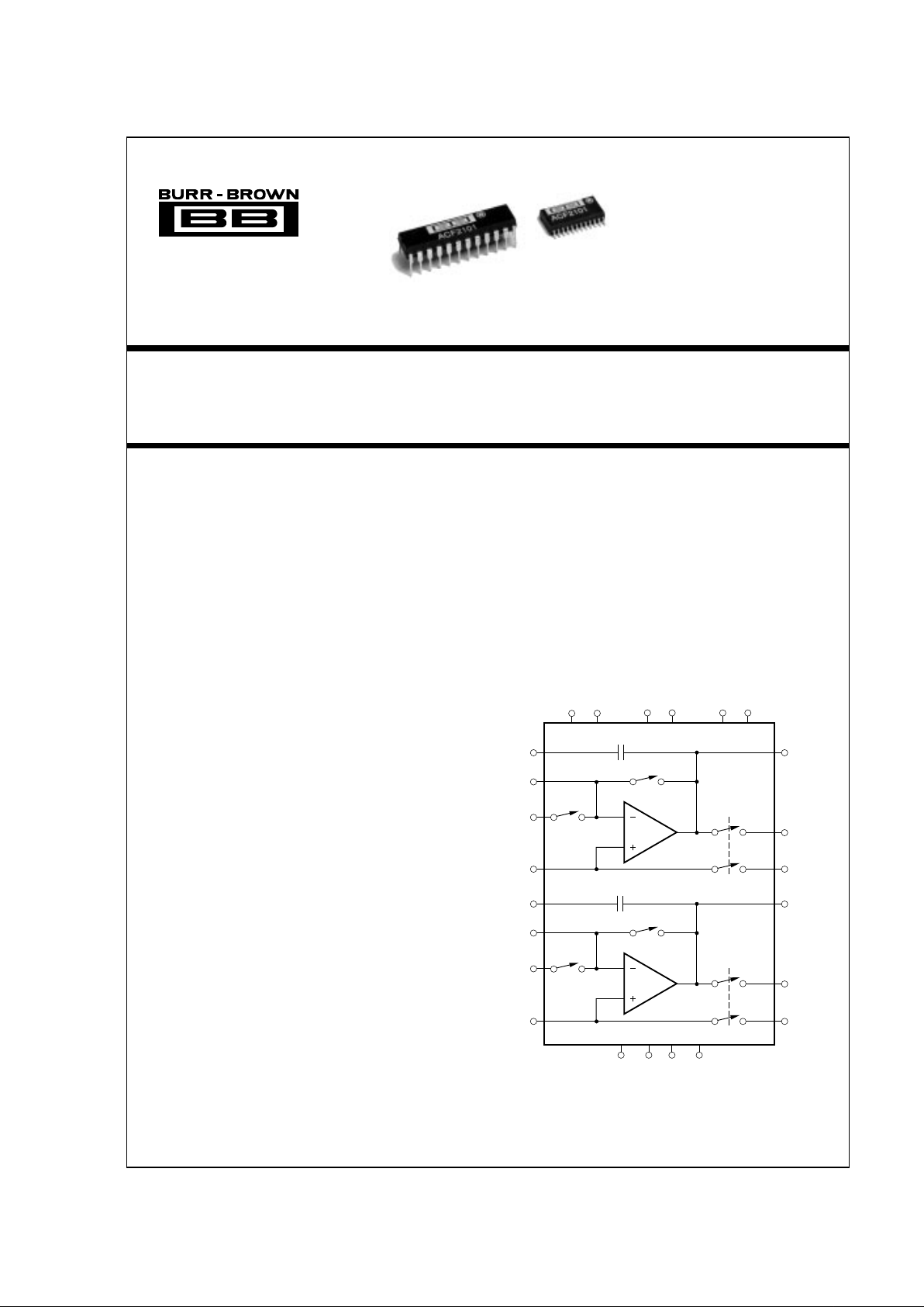
ACF2101
Low Noise, Dual
SWITCHED INTEGRATOR
A B
A B
V+ Gnd V–
Sw In B
Hold
Sw In A
Cap A
In A
Com A Sw Com A
Sw Out A
Out A
100pF
Cap B
In B
Com B Sw Com B
Sw Out B
Out B
A
B
Reset Hold Select
100pF
A B A B
Hold
Reset
Reset
Select
Select
C
INTERNAL
C
INTERNAL
APPLICATIONS
● CURRENT TO VOLTAGE CONVERSION
● PHOTODIODE INTEGRATOR
● CURRENT MEASUREMENT
● CHARGE MEASUREMENT
● CT SCANNER FRONT END
● MEDICAL, SCIENTIFIC, AND INDUSTRIAL
INSTRUMENTATION
DESCRIPTION
The ACF2101 is a dual switched integrator for precision applications. Each channel can convert an input
current to an output voltage by integration, using either
an internal or external capacitor. Included on the chip
are precision 100pF integration capacitors, hold and
reset switches, and output multiplexers.
As a complete circuit on a single chip, the ACF2101
eliminates many of the problems commonly encountered in discrete designs, such as leakage current errors
and noise pickup. The integrating approach can provide lower noise than conventional transimpedance
amplifier designs and also eliminates the need for high
performance, high value feedback resistors.
The extremely low bias current and low noise of the
ACF2101’s
Difet®
amplifiers, along with active laser trimming of both offset and drift, assure precision
current to voltage conversion.
Although designed for +5V, –15V supplies, the
ACF2101 can be operated on supplies up to ±18VDC.
It is available in both 24-pin plastic DIP and SOIC
packages.
Difet
®
Burr-Brown Corp.
FEATURES
● INCLUDES INTEGRATION CAPACITOR,
RESET AND HOLD SWITCHES, AND
OUTPUT MULTIPLEXER
● LOW NOISE: 10µVrms
● LOW CHARGE TRANSFER: 0.1pC
● WIDE DYNAMIC RANGE: 120dB
● LOW BIAS CURRENT: 100fA
FPO
© 1990 Burr-Brown Corporation PDS-1078D Printed in U.S.A. September, 1994

®
ACF2101
2
V
OUT
= – I
IN
dt
SPECIFICATIONS
ELECTRICAL
At TA = +25°C, V+ = +5V, V– = –15V, Internal C
INTEGRATION
= C
INTERNAL
= 100pF, unless otherwise noted.
C
INTEGRATION
The information provided herein is believed to be reliable; however, BURR-BROWN assumes no responsibility for inaccuracies or omissions. BURR-BROWN assumes
no responsibility for the use of this information, and all use of such information shall be entirely at the user’s own risk. Prices and specifications are subject to change
without notice. No patent rights or licenses to any of the circuits described herein are implied or granted to any third party. BURR-BROWN does not authorize or warrant
any BURR-BROWN product for use in life support devices and/or systems.
1
∫
ACF2101BP, BU
PARAMETER CONDITIONS MIN TYP MAX UNITS
ANALOG INPUT
INPUT RANGE
Input Current Range
Switched Input (S
W IN A, SW IN B) ±100 µA
Direct Input (I
N A, IN B) ±100 µA
INPUT IMPEDANCE
Switched Input
Hold Switch OFF 1000 GΩ
Hold Switch ON 1.5 kΩ
Direct Input Virtual Ground
HOLD SWITCH VOLTAGE
Hold Switch Withstand Voltage Hold Switch OFF –10 +0.5 V
OFFSET VOLTAGE
Input Offset Voltage ±0.5 ±2mV
Average Drift ±1 ±5 µV/°C
DIGITAL INPUTS
Logic Family TTL Compatible
V
IH
(Logic 1 = Switch OFF) 2 5.5 V
V
IL
(Logic 0 = Switch ON) –0.5 0.8 V
I
IH
VIH = +5V 2 µA
I
IL
VIL = 0V 0 µA
Switching Speed (All Switches)
Switch ON 200 ns
Switch OFF 200 ns
TRANSFER CHARACTERISTICS
TRANSFER FUNCTION V
DYNAMIC CHARACTERISTICS
Integrate Mode
Slew Rate 13 V/µs
Reset Mode
Slew Rate 3V/µs
Settling Time to 0.01%FSR
(1)
10V Step 5 10 µs
Overload Recovery Positive or Negative 5 µs
Output Multiplexer (Select Switches)
Settling Time to 0.01%FSR C
LOAD
< 1000pF 6.5 µs
Settling Time to 0.01%FSR C
LOAD
< 100pF 2 µs
INTEGRATION CAPACITOR (C
INTERNAL
)
Internal Capacitor
Value 100 pF
Accuracy 0.5 2 %
Temperature Coefficient –50 –25 0 ppm/°C
Memory 30 100 ppm of FSR
RESET SWITCH
Impedance
Reset OFF 1000 GΩ
Reset ON 1.5 kΩ
MODES OF OPERATION
Switch Hold Reset
Integrate Mode ON OFF
Hold Mode OFF OFF
Reset Mode ON/OFF ON
(Logic 1 = OFF, Logic 0 = ON)
®
ACF2101
3
SPECIFICATIONS (CONT)
At TA = +25°C, V+ = +5V, V– = –15V, Internal C
INTEGRATION
= C
INTERNAL
= 100pF, unless otherwise noted.
ACF2101BP, BU
PARAMETER CONDITIONS MIN TYP MAX UNITS
OUTPUT
Voltage Output Range (All Outputs) –10 –13.5, +1.0 +0.5 V
Current Output, Direct Output (Out A, Out B) ±5mA
Short Circuit Current
Direct Output ±25 mA
Switched Output (Sw Out A, Sw Out B) ±2 ±8mA
Select Switch Withstand Voltage
Switched Output –10 +0.5 V
Switched Common (Sw Com A, Sw Com B) –0.5 +0.5 V
Output Impedance
Direct Output 0.1 Ω
Switched Output
Select Switch ON 250 || 5 Ω || pF
Select Switch OFF 1000 || 4 GΩ || pF
Leakage Current Select Switch OFF 10 100 pA
Load Capacitance Stability
Direct Output 500 pF
Switched Output Any pF
OUTPUT ACCURACY
Nonlinearity ±0.005 ±0.01 %FSR
Channel Separation –80 dB
Op Amp Bias Current
Value 100 1000 fA
Temperature Coefficient Doubles Each +10°C
Hold Mode Droop 1 10 nV/µs
Integrate Mode Droop 1 10 nV/µs
Voltage Offset
(2)
Value 3mV
Temperature Coefficient 5 µV/°C
Power Supply Rejection V
S
= +4.5V to +18V, –10V to –18V 80 100 dB
OUTPUT NOISE
Total Output Noise
(3)
BW = 0.1Hz to 10Hz 2 µVrms
Integrate Mode
(4)
BW = 0.1Hz to 250kHz 10(1 + CIN/C
INTEGRATION
) µVrms
Hold Mode BW = 0.1Hz to 250kHz 10 µVrms
Reset Mode BW = 0.1Hz to 250kHz 10 µVrms
CHARGE TRANSFER ERRORS
(5)
Reset to Integrate Mode
(6)
Charge Transfer 0.1 0.5 pC
Charge Transfer TC 0.2 fC/°C
Charge Offset Error 15mV
Charge Offset TC 2 µV/°C
Integrate to Hold Mode C
IN
> 50pF
Charge Transfer 0.2 1 pC
Charge Transfer TC 0.4 fC/°C
Charge Offset Error 210mV
Charge Offset TC 4 µV/°C
Hold to Integrate Mode C
IN
> 50pF
Charge Transfer 0.2 1 pC
Charge Transfer TC 0.4 fC/°C
Charge Offset Error 210mV
Charge Offset TC 4 µV/°C
POWER SUPPLY
Specified Operating Voltage +5, –15 V
Operating Voltage Range
Positive Supply +4.5 +18 V
Negative Supply –10 –18 V
Current
Positive Supply For Dual 12 15 mA
Negative Supply For Dual 3.5 5.2 mA
TEMPERATURE RANGE
Specification –40 +85 °C
Operation –40 +125 °C
Storage –40 +125 °C
Thermal Resistance (both packages) Junction to Ambient 100 °C/W
NOTES: (1) FSR is Full Scale Range = 10V (0 to –10V). (2) Includes offset errors from all modes of operation. (3) Total noise is rms total of noise for the modes
of operation used. (4) C
IN
= capacitance of sensor connected to ACF2101 input; C
INTERGRATION
= integration capacitance = C
INTERNAL
+ C
EXTERNAL
. (5) Errors created
when the internal switches are driven from one mode to another. (6) The charge transfer is 0.1pC; for an integration capacitance of 100pF, the resultant charge
offset voltage error is 1mV.
®
ACF2101
4
ABSOLUTE MAXIMUM RATINGS
Supply ...............................................................................................±18V
Input Current ..................................................................................... ±5mA
Output Short Circuit Duration .................................. Continuous to Ground
Power Dissipation .......................................................................... 500mW
Operating Temperature................................................... –40°C to +125°C
Storage Temperature ...................................................... –40°C to +125°C
Junction Temperature .................................................................... +150°C
Lead Temperature (soldering, 10s)................................................ +300°C
ELECTROSTATIC
DISCHARGE SENSITIVITY
Electrostatic discharge can cause damage ranging from performance degradation to complete device failure. BurrBrown Corporation recommends that all integrated circuits
be handled and stored using appropriate ESD protection
methods.
PACKAGE
DRAWING TEMPERATURE
PRODUCT PACKAGE NUMBER
(1)
RANGE
ACF2101BP 24-Pin Plastic DIP 243 –40°C to +85°C
ACF2101BU 24-Pin Plastic SOIC 239 –40°C to +85°C
NOTE: (1) For detailed drawing and dimension table, please see end of data
sheet, or Appendix C of Burr-Brown IC Data Book.
PACKAGE/ORDERING INFORMATION
TOP VIEW ACF2101BU
PIN CONFIGURATION
DIP and SOIC package have different pinouts.
TOP VIEW ACF2101BP
1
2
3
4
5
6
7
8
9
10
11
12
24
23
22
21
20
19
18
17
16
15
14
13
DIP
Out A
Gnd A
Com A
Cap A
In A
Sw In A
Sw In B
In B
Cap B
Com B
Gnd B
Out B
Sw Out A
Sw Com A
Select A
Reset A
Hold A
V+
V–
Hold B
Reset B
Select B
Sw Com B
Sw Out B
1
2
3
4
5
6
7
8
9
10
11
12
24
23
22
21
20
19
18
17
16
15
14
13
Sw In B
In B
Cap B
Com B
Gnd B
Out B
Sw Out B
Sw Com B
Select B
Reset B
Hold B
V–
Sw In A
In A
Cap A
Com A
Gnd A
Out A
Sw Out A
Sw Com A
Select A
Reset A
Hold A
V+
SOIC
®
ACF2101
5
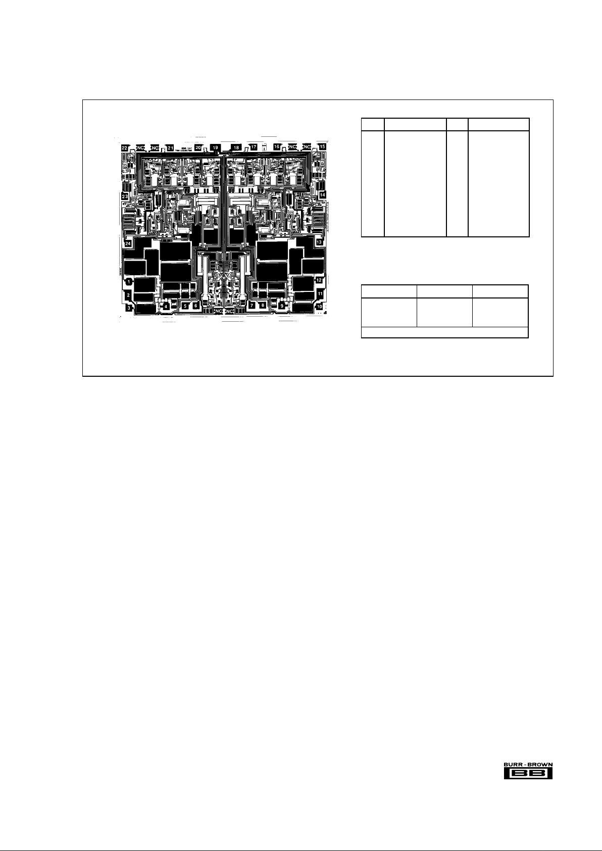
PAD FUNCTION
13 B Switch-Out
14 B Switch-Common
15 B Select
16 B Reset
17 B Hold
18 V–
19 V+
20 A Hold
21 A Reset
22 A Select
23 A Switch-Common
24 A Switch-Out
DICE INFORMATION
PAD FUNCTION
1 A Out
2 A Ground
3 A Common
4 A Cap
5 A In
6 A Switch-In
7 B Switch-In
8 B In
9 B Cap
10 B Common
11 B Ground
12 B Out
Substrate Bias: Ground.
MECHANICAL INFORMATION
MILS (0.001") MILLIMETERS
Die Size 132 x 157 ±5 3.35 x 3.99 ±0.13
Die Thickness 20 ±3 0.51 ±0.08
Min. Pad Size 4 x 4 0.10 x 0.10
Backing None
ACF2101 DIE TOPOGRAPHY
 Loading...