

Burr Brown XTR106UA-2K5, XTR106UA, XTR106U, XTR106U-2K5, XTR106PA Datasheet
...
®
XTR106
XTR106
XTR106
4-20mA CURRENT TRANSMITTER
with Bridge Excitation and Linearization
FEATURES
● LOW TOTAL UNADJUSTED ERROR
● 2.5V, 5V BRIDGE EXCITATION REFERENCE
● 5.1V REGULATOR OUTPUT
● LOW SPAN DRIFT: ±25ppm/°C max
● LOW OFFSET DRIFT: 0.25µV/°C
● HIGH PSR: 110dB min
● HIGH CMR: 86dB min
● WIDE SUPPLY RANGE: 7.5V to 36V
● 14-PIN DIP AND SO-14 SURFACE-MOUNT
DESCRIPTION
The XTR106 is a low cost, monolithic 4-20mA, twowire current transmitter designed for bridge sensors. It
provides complete bridge excitation (2.5V or 5V reference), instrumentation amplifier, sensor linearization,
and current output circuitry. Current for powering additional external input circuitry is available from the
V
pin.
REG
The instrumentation amplifier can be used over a wide
range of gain, accommodating a variety of input signal
types and sensors. Total unadjusted error of the complete current transmitter, including the linearized bridge,
is low enough to permit use without adjustment in many
applications. The XTR106 operates on loop power supply voltages down to 7.5V.
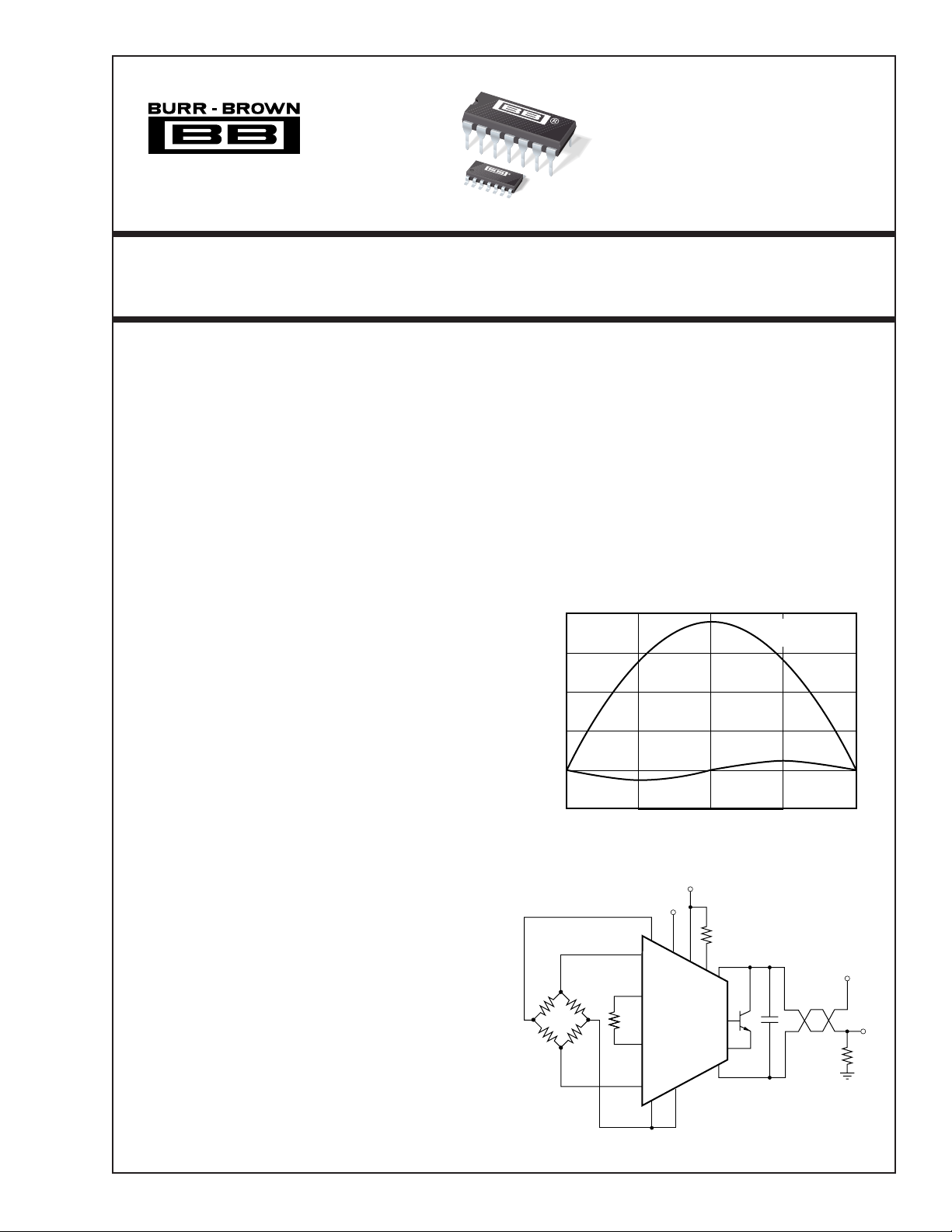
Linearization circuitry provides second-order correction
to the transfer function by controlling bridge excitation
voltage. It provides up to a 20:1 improvement in
nonlinearity, even with low cost transducers.
The XTR106 is available in 14-pin plastic DIP and
SO-14 surface-mount packages and is specified for the
–40°C to +85°C temperature range. Operation is from
–55°C to +125°C.
APPLICATIONS
● PRESSURE BRIDGE TRANSMITTER
● STRAIN GAGE TRANSMITTER
● TEMPERATURE BRIDGE TRANSMITTER
● INDUSTRIAL PROCESS CONTROL
● SCADA REMOTE DATA ACQUISITION
● REMOTE TRANSDUCERS
● WEIGHING SYSTEMS
● ACCELEROMETERS
2.0
1.5
1.0
0.5
Nonlinearity (%)
–0.5
5V
0
0mV
BRIDGE NONLINEARITY CORRECTION
V
5
REF
R
V
REF
+
G
USING XTR106
5mV
Bridge Output
(5.1V)
V
REG
2.5V
XTR106
Corrected
R
LIN
7.5V to 36V
Uncorrected
Bridge Output
4-20mA
10mV
V
PS
V
O
R
L
–
I
RET
International Airport Industrial Park • Mailing Address: PO Box 11400, Tucson, AZ 85734 • Street Address: 6730 S. Tucson Blvd., Tucson, AZ 85706 • Tel: (520) 746-1111 • Twx: 910-952-1111
Internet: http://www.burr-brown.com/ • FAXLine: (800) 548-6133 (US/Canada Only) • Cable: BBRCORP • Telex: 066-6491 • FAX: (520) 889-1510 • Immediate Product Info: (800) 548-6132
©
1998 Burr-Brown Corporation PDS-1449A Printed in U.S.A. June, 1998
Polarity
Lin
I
OUT

SPECIFICATIONS
At TA = +25°C, V+ = 24V, and TIP29C external transistor, unless otherwise noted.
XTR106P, U XTR106PA, UA
PARAMETER CONDITIONS MIN TYP MAX MIN TYP MAX UNITS
OUTPUT
Output Current Equation I
Output Current, Specified Range 4 20 ✻✻mA
Over-Scale Limit I
Under-Scale Limit I
ZERO OUTPUT
(1)
Initial Error ±5 ±25 ✻ ±50 µA
vs Temperature T
vs Supply Voltage, V+ V+ = 7.5V to 36V 0.04 0.2 ✻✻ µA/V
vs Common-Mode Voltage
(IO) 0.8 ✻ µA/mA
vs V
REG
Noise: 0.1Hz to 10Hz i
(CMRR)
OVER
UNDER
I
ZERO
O
I
= 0, I
I
REF
REG
+ I
= 0 1 1.6 2.2 ✻✻✻ mA
REF
= 2.5mA 2.9 3.4 4 ✻✻✻ mA
REG
VIN = 0V, RG = ∞ 4 ✻ mA
= –40°C to +85°C ±0.07 ±0.9 ✻✻ µA/°C
A
VCM = 1.1V to 3.5V
n
(5)
SPAN
Span Equation (Transconductance) S
Untrimmed Error Full Scale (V
vs Temperature
Nonlinearity: Ideal Input
INPUT
Offset Voltage V
vs Temperature T
vs Supply Voltage, V+ V+ = 7.5V to 36V ±0.1 ±3 ✻✻ µV/V
vs Common-Mode Voltage, RTI CMRR V
Common-Mode Range
Input Bias Current I
vs Temperature T
Input Offset Current I
vs Temperature T
Impedance: Differential Z
Noise: 0.1Hz to 10Hz V
VOLTAGE REFERENCES
(2)
(3)
(4)
(5)
Common-Mode 5 || 10 ✻ GΩ || pF
(5)
TA = –40°C to +85°C ±3 ±25 ✻✻ ppm/°C
Full Scale (VIN) = 50mV ±0.001 ±0.01 ✻✻ %
OS
V
CM
OS
IN
= –40°C to +85°C ±0.25 ±1.5 ✻ ±3 µV/°C
A
CM
B
= –40°C to +85°C20 ✻ pA/°C
A
= –40°C to +85°C5 ✻pA/°C
A
n
Lin Polarity Connected
to V
Initial: 2.5V Reference V
5V Reference V
Accuracy V
vs Temperature T
vs Supply Voltage, V+ V+ = 7.5V to 36V ±5 ±20 ✻✻ ppm/V
vs Load I
Noise: 0.1Hz to 10Hz 10 ✻ µVp-p
(5)
V
REG
Accuracy ±0.02 ±0.1 ✻✻ V
vs Temperature T
vs Supply Voltage, V+ V+ = 7.5V to 36V 1 ✻ mV/V
Output Current I
Output Impedance I
LINEARIZATION
R
(external) Equation R
LIN
K
Linearization Factor K
LIN
(6)
2.5 2.5 ✻ V
REF
55✻V
V
REF
REG
REG
LIN
LIN
REF
= –40°C to +85°C ±20 ±35 ✻ ±75 ppm/°C
A
REF
= –40°C to +85°C ±0.3 ✻ mV/°C
A
REG
Accuracy ±1 ±5 ✻✻ %
vs Temperature T
Max Correctable Sensor Nonlinearity B V
= –40°C to +85°C ±50 ±100 ✻✻ ppm/°C
A
) = 50mV ±0.05 ±0.2 ✻ ±0.4 %
IN
VCM = 2.5V ±50 ±100 ✻ ±250 µV
= 1.1V to 3.5V
, R
REG
(5)
= 0
LIN
= 2.5V or 5V ±0.05 ±0.25 ✻ ±0.5 %
= 0mA to 2.5mA 60 ✻ ppm/mA
= 0mA to 2.5mA 80 ✻ Ω
V
= 5V 6.645 ✻ k Ω
REF
= 2.5V 9.905 ✻ k Ω
V
REF
= 5V ±5 ✻ % of V
REF
V
= 2.5V –2.5, +5 ✻ % of V
REF
POWER SUPPLY V+
Specified +24 ✻ V
Voltage Range +7.5 +36 ✻✻V
TEMPERATURE RANGE
Specification –40 +85 ✻✻°C
Operating –55 +125 ✻✻°C
Storage –55 +125 ✻✻°C
Thermal Resistance
14-Pin DIP 80 ✻ °C/W
θ
JA
SO-14 Surface Mount 100 ✻ °C/W
✻ Specification same as XTR106P, XTR106U.
NOTES: (1) Describes accuracy of the 4mA low-scale offset current. Does not include input amplifier effects. Can be trimmed to zero. (2) Does not include initial
error or TCR of gain-setting resistor, R
measured with respect to I
®
pin. (6) See “Linearization” text for detailed explanation. VFS = full-scale VIN.
RET
. (3) Increasing the full-scale input range improves nonlinearity. (4) Does not include Zero Output initial error. (5) Voltage
G
XTR106
IO = VIN • (40/RG) + 4mA, VIN in Volts, RG in Ω
A
24 28 30 ✻✻✻ mA
0.02 ✻ µA/V
0.035 ✻ µAp-p
S = 40/R
G
✻ A/V
±10 ±50 ✻ ±100 µV/V
1.1 3.5 ✻✻V
525 ✻50 nA
±0.2 ±3 ✻ ±10 nA
0.1 || 1 ✻ GΩ || pF
0.6 ✻ µVp-p
5.1 ✻ V
See Typical Curves ✻ mA
R
= K
LIN
4B
• , K
LIN
1 – 2B
in Ω, B is nonlinearity relative to V
LIN
FS
Ω
FS
FS
2
PIN CONFIGURATION
Top View DIP and SOIC
1
V
REG
–
2
V
IN
3
R
G
4
R
G
+
5
V
IN
6
I
RET
7
I
O
14
13
12
11
10
9
8
V
5
REF
2.5
V
REF
Lin Polarity
R
LIN
V+
B (Base)
E (Emitter)
ABSOLUTE MAXIMUM RATINGS
Power Supply, V+ (referenced to IO pin) .......................................... 40V
Input Voltage, V
Storage Temperature Range ........................................ –55°C to +125°C
Lead Temperature (soldering, 10s).............................................. +300 °C
Output Current Limit ............................................................... Continuous
Junction Temperature................................................................... +165 °C
NOTE: (1) Stresses above these ratings may cause permanent damage.
Exposure to absolute maximum conditions for extended periods may degrade
device reliability.
+
–
, VIN (referenced to I
IN
(1)
pin) ......................... 0V to V+
RET
ELECTROSTATIC
DISCHARGE SENSITIVITY
This integrated circuit can be damaged by ESD. Burr-Brown
recommends that all integrated circuits be handled with
appropriate precautions. Failure to observe proper handling
and installation procedures can cause damage.
ESD damage can range from subtle performance degradation
to complete device failure. Precision integrated circuits may
be more susceptible to damage because very small parametric
changes could cause the device not to meet its published
specifications.
PACKAGE/ORDERING INFORMATION
PACKAGE SPECIFIED
DRAWING TEMPERATURE PACKAGE ORDERING TRANSPORT
PRODUCT PACKAGE NUMBER
XTR106P 14-Pin DIP 010 –40°C to +85°C XTR106P XTR106P Rails
XTR106PA 14-Pin DIP 010 –40°C to +85°C XTR106PA XTR106PA Rails
XTR106U SO-14 Surface Mount 235 –40°C to +85°C XTR106U XTR106U Rails
(1)
RANGE MARKING NUMBER
"""""XTR106U/2K5 Tape and Reel
XTR106UA SO-14 Surface Mount 235 –40°C to +85°C XTR106UA XTR106UA Rails
"""""XTR106UA/2K5 Tape and Reel
NOTES: (1) For detailed drawing and dimension table, please see end of data sheet, or Appendix C of Burr-Brown IC Data Book. (2) Models with a slash (/ ) are
available only in Tape and Reel in the quantities indicated (e.g., /2K5 indicates 2500 devices per reel). Ordering 2500 pieces of “XTR106U/2K5” will get a single
2500-piece Tape and Reel. For detailed Tape and Reel mechanical information, refer to Appendix B of Burr-Brown IC Data Book.
(2)
MEDIA
The information provided herein is believed to be reliable; however, BURR-BROWN assumes no responsibility for inaccuracies or omissions. BURR-BROWN assumes
no responsibility for the use of this information, and all use of such information shall be entirely at the user’s own risk. Prices and specifications are subject to change
without notice. No patent rights or licenses to any of the circuits described herein are implied or granted to any third party. BURR-BROWN does not authorize or warrant
any BURR-BROWN product for use in life support devices and/or systems.
3
XTR106
®
FUNCTIONAL DIAGRAM
Lin
Polarity
V
REG
12
R
LIN
11
1
V+
10
14
V
5
REF
13
2.5
V
REF
5
+
V
IN
4
REF
Amp
Bandgap
V
REF
100µA
Lin
Amp
Current
Direction
Switch
5.1V
B
9
R
G
975
3
V
2
–
V
IN
I = 100µA +
IN
R
G
25
Ω
Ω
E
8
®
XTR106
6
I
RET
7
= 4mA + V
I
O
• ( )
IN
40
R
G
4
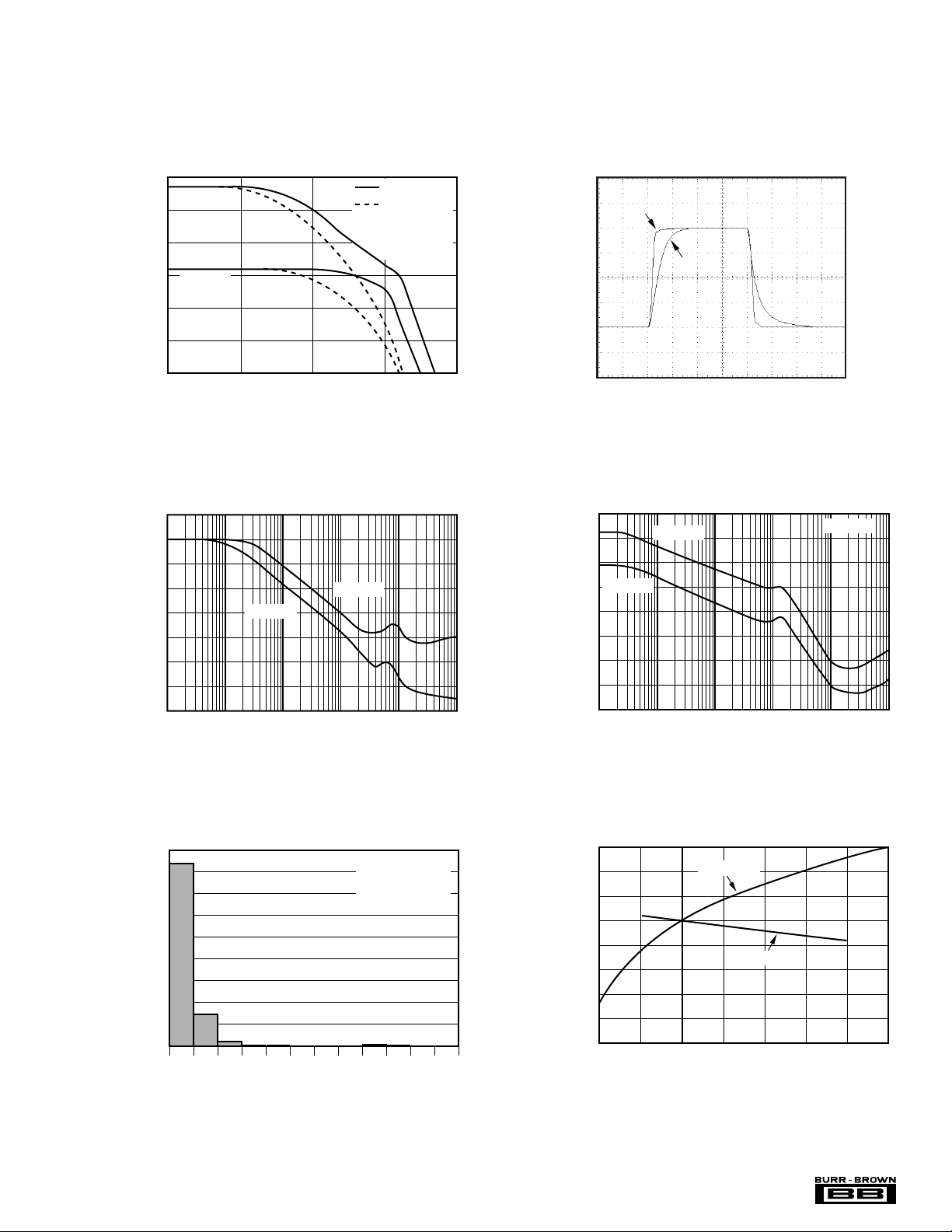
TYPICAL PERFORMANCE CURVES
10 1k100 10k 100k 1M
Frequency (Hz)
POWER SUPPLY REJECTION vs FREQUENCY
160
140
120
100
80
60
40
20
0
Power Supply Rejection (dB)
RG = 1kΩ
C
OUT
= 0
RG = 50Ω
At TA = +25°C, V+ = 24V, unless otherwise noted.
60
RG = 50Ω
50
40
30
RG = 1kΩ
C
C
OUT
C
OUT
connected
C
OUT
between V+ and I
20
TRANSCONDUCTANCE vs FREQUENCY
10
Transconductance (20 log mA/V)
R
= 250Ω
L
0
100 1k 10k 100k 1M
Frequency (Hz)
COMMON-MODE REJECTION vs FREQUENCY
110
100
90
80
70
RG = 1kΩ
RG = 50Ω
60
50
Common-Mode Rejection (dB)
40
30
10 1k100 10k 100k 1M
Frequency (Hz)
= 0.01µF
= 0.01µF
OUT
= 0.033µF
STEP RESPONSE
C
= 0.01µF
RG = 1kΩ
OUT
20mA
O
RG = 50Ω
4mA/div
4mA
50µs/div
INPUT OFFSET VOLTAGE DRIFT
90
PRODUCTION DISTRIBUTION
80
70
60
50
40
30
Percent of Units (%)
20
10
0
0
0.25
0.5
0.75
1.0
Offset Voltage Drift (µV/°C)
INPUT OFFSET VOLTAGE CHANGE
Typical production
distribution of
packaged units.
1.5
1.0
0.5
vs V
REG
VOS vs I
and V
CURRENTS
REF
REG
0
(µV)
–0.5
OS
∆ V
–1.0
–1.5
VOS vs I
REF
–2.0
–2.5
–1.0 –0.5 0 0.5 1.0 1.5 2.0 2.5
1.25
1.5
1.75
2.0
2.25
2.5
2.75
3.0
5
Current (mA)
®
XTR106
 Loading...