

Burr Brown XTR104BU, XTR104BP, XTR104AU-1K, XTR104AU, XTR104AP Datasheet
1
®
XTR104
International Airport Industrial Park • Mailing Address: PO Box 11400 • Tucson, AZ 85734 • Street Address: 6730 S. Tucson Blvd. • Tucson, AZ 85706
Tel: (520) 746-1111 • Twx: 910-952-1111 • Cable: BBRCORP • Telex: 066-6491 • FAX: (520) 889-1510 • Immediate Product Info: (800) 548-6132
XTR104
4-20mA Current Transmitter with
BRIDGE EXCITATION AND LINEARIZATION
APPLICATIONS
● INDUSTRIAL PROCESS CONTROL
● FACTORY AUTOMATION
● SCADA
● WEIGHTING SYSTEMS
● ACCELEROMETERS
FEATURES
● LESS THAN ±1% TOTAL ADJUSTED
ERROR, –40
°C TO +85°C
● BRIDGE EXCITATION AND LINEARIZATION
● WIDE SUPPLY RANGE: 9V to 40V
● LOW SPAN DRIFT: 50ppm/
°C max
● HIGH PSR: 110dB min
● HIGH CMR: 80dB min
DESCRIPTION
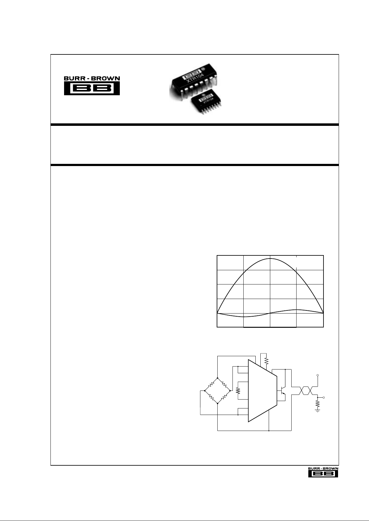
The XTR104 is a monolithic 4-20mA, two-wire current transmitter integrated circuit designed for bridge
input signals. It provides complete bridge excitation,
instrumentation amplifier, linearization, and current
output circuitry necessary for high impedance strain
gage sensors.
The instrumentation amplifier can be used over a wide
range of gain, accommodating a variety of input signals
and sensors. Total adjusted error of the complete current
transmitter, including the linearized bridge is less than
±1% over the full –40°C to +85°C temperature range.
This includes zero drift, span drift and non-linearity for
bridge outputs as low as 10mV. The XTR104 operates
on loop power supply voltages down to 9V.
Linearization circuitry consists of a second, fully independent instrumentation amplifier that controls the bridge
excitation voltage. It provides second-order correction
to the transfer function, typically achieving a 20:1
improvement in nonlinearity, even with low cost transducers.
The XTR104 is available in 16-pin plastic DIP and
SOL-16 surface-mount packages specified for the
–40°C to +85°C temperature range.
XTR104
R
G
R
L
4-20 mA
R
LIN
9V to 40V
–
+
V
O
V
PS
BRIDGE NONLINEARITY CORRECTION
USING XTR104
0mV
Bridge Output
10mV
2.0
1.5
1.0
0.5
0
–0.5
Uncorrected
Bridge Output
Corrected
5mV
Nonlinearity (%)
®
©
1992 Burr-Brown Corporation PDS-1146B Printed in U.S.A. September, 1993

2
®
XTR104
XTR104BP, BU XTR104AP, AU
PARAMETER CONDITIONS MIN TYP MAX MIN TYP MAX UNITS
OUTPUT
Output Current Equation A
Total Adjusted Error
(1)
T
MIN
to T
MAX
, VFS ≥ 10mV, RB = 5kΩ±1 ±2 % of FS
Current, Specified Range 4 20 * * mA
Over-Scale Limit 34 40 * * mA
Under Scale-Limit 3.6 3.8 * * mA
Full Scale Output Error V
IN
= 1V, RG = ∞±15 ±50 * ±100 µA
Noise: 0.1Hz to 1kHz R
G
= 40Ω 8*µAp-p
ZERO OUTPUT
(2)
VIN = 0V, RG = ∞ 4*mA
Initial Error ±5 ±50 * ±100 µA
vs Temperature ±0.2 ±0.5 * ±1 µA/°C
vs Supply Voltage, V+ V+ = 9V to 40V
(3)
0.5 2 * * µA/V
vs Common-Mode Voltage V
CM
= 2V to 3V
(3)
0.1 2 * * µA/V
SPAN
Span Equation (Transconductance) * A/V
Untrimmed Error R
G
≥ 75Ω±0.1 ±1**%
vs Temperature
(4)
±20 ±50 * ±100 ppm/°C
Nonlinearity: Ideal Input 0.01 * %
Bridge Input
(5)
0.1 * %
INPUT
Differential Range 1*V
Input Voltage Range
(3)
23**V
Common-Mode Rejection V
IN
= 2V to 3V
(3)
80 100 * * dB
Impedance: Differential 3 * GΩ
Common-Mode 0.5 * GΩ
Offset Voltage ±0.5 ±2.5 * * mV
vs Temperature 1 2.5 2 5 µV/°C
vs Supply Voltage, V+ V+ = 9V to 40V
(3)
110 130 * * dB
Input Bias Current 100 250 * * nA
vs Temperature 0.1 2 * * nA/°C
Input Offset Current 2 20 * * nA
vs Temperature 0.01 0.25 * * nA/°C
VOLTAGE REFERENCE
(6)
Voltage 5*V
Accuracy ±0.25 ±0.5 * ±1%
vs Temperature ±10 ±50 * ±100 ppm/°C
vs Supply Voltage, V+ V+ = 9V to 40V
(3)
5 * ppm/V
vs Load I
L
= 0 to 2mA 50 * ppm/mA
POWER SUPPLY
Voltage Range
(3)
, V+ 9 40 * * V
TEMPERATURE RANGE
Specification (T
MIN
to T
MAX
) –40 85 * * °C
Operating Derated Performance –40 125 * * °C
θ
JA
80 * °C/W
IO = VIN • (0.016 + 40/RG) + 4mA VIN in Volts, RG in Ω
* Specification same as XTR104BP.
NOTES: (1) Includes corrected second-order nonlinearity of bridge, and over-temperature zero and span effects. Does not include initial offset and span errors which
are normally trimmed to zero at 25°C. (2) Describes accuracy of the 4mA low-scale current. Does not include input amplifier effects. Can be trimmed to zero.
(3) Voltage measured with respect to I
O
pin. (4) Does not include TCR of gain-setting resistor, RG. (5) When configured to correct for ≤2% second-order bridge sensor
nonlinearity. (6) Measured with R
LIN
= ∞ to disable linearization feature.
S = 0.016 + 40/R
G
SPECIFICATIONS
TA = +25°C, V+ = 24V, and 2N6121 external transistor, unless otherwise noted.
3
®
XTR104
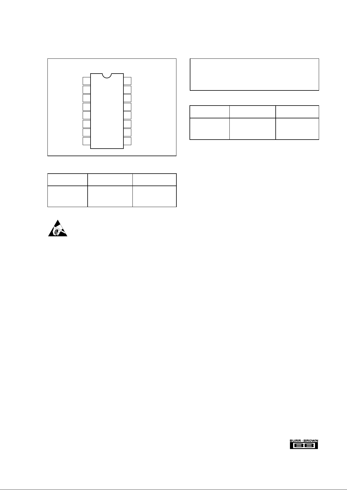
ABSOLUTE MAXIMUM RATINGSPIN CONFIGURATION
Power Supply, V+ (referenced to IO pin) .......................................... 40V
Input Voltage, V
+
IN
, V
–
IN
, V
+
LIN
, V
–
LIN
(referenced to IO pin) ... 0V to V+
Storage Temperature Range ........................................ –55°C to +125°C
Lead Temperature (soldering, 10s).............................................. +300°C
Output Current Limit ............................................................... Continuous
Junction Temperature ................................................................... +165°C
The information provided herein is believed to be reliable; however, BURR-BROWN assumes no responsibility for inaccuracies or omissions. BURR-BROWN assumes
no responsibility for the use of this information, and all use of such information shall be entirely at the user’s own risk. Prices and specifications are subject to change
without notice. No patent rights or licenses to any of the circuits described herein are implied or granted to any third party. BURR-BROWN does not authorize or warrant
any BURR-BROWN product for use in life support devices and/or systems.
V
+
IN
V
–
IN
V
+
LIN
V
–
LIN
R
G
R
G
I
O
R
LIN
Zero Adjust
Zero Adjust
Zero Adjust
B (Base)
V
REF
E (Emitter)
V+
R
LIN
1
2
3
4
5
6
7
8
16
15
14
13
12
11
10
9
PACKAGE INFORMATION
PACKAGE DRAWING
MODEL PACKAGE NUMBER
(1)
XTR104AP 16-Pin Plastic DIP 180
XTR104BP 16-Pin Plastic DIP 180
XTR104AU SOL-16 Surface Mount 211
XTR104BU SOL-16 Surface Mount 211
NOTE: (1) For detailed drawing and dimension table, please see end of data
sheet, or Appendix D of Burr-Brown IC Data Book.
TEMPERATURE
MODEL PACKAGE RANGE
XTR104AP 16-pin Plastic DIP –40°C to +85°C
XTR104BP 16-pin Plastic DIP –40°C to +85°C
XTR104AU SOL-16 Surface Mount –40°C to +85°C
XTR104BU SOL-16 Surface Mount –40°C to +85°C
ORDERING INFORMATION
Top View DIP
ELECTROSTATIC
DISCHARGE SENSITIVITY
Electrostatic discharge can cause damage ranging from performance degradation to complete device failure. Burr-Brown
Corporation recommends that all integrated circuits be handled
and stored using appropriate ESD protection methods.
ESD damage can range from subtle performance degradation
to complete device failure. Precision integrated circuits may
be more susceptible to damage because very small parametric
changes could cause the device not to meet published specifications.
4
®
XTR104
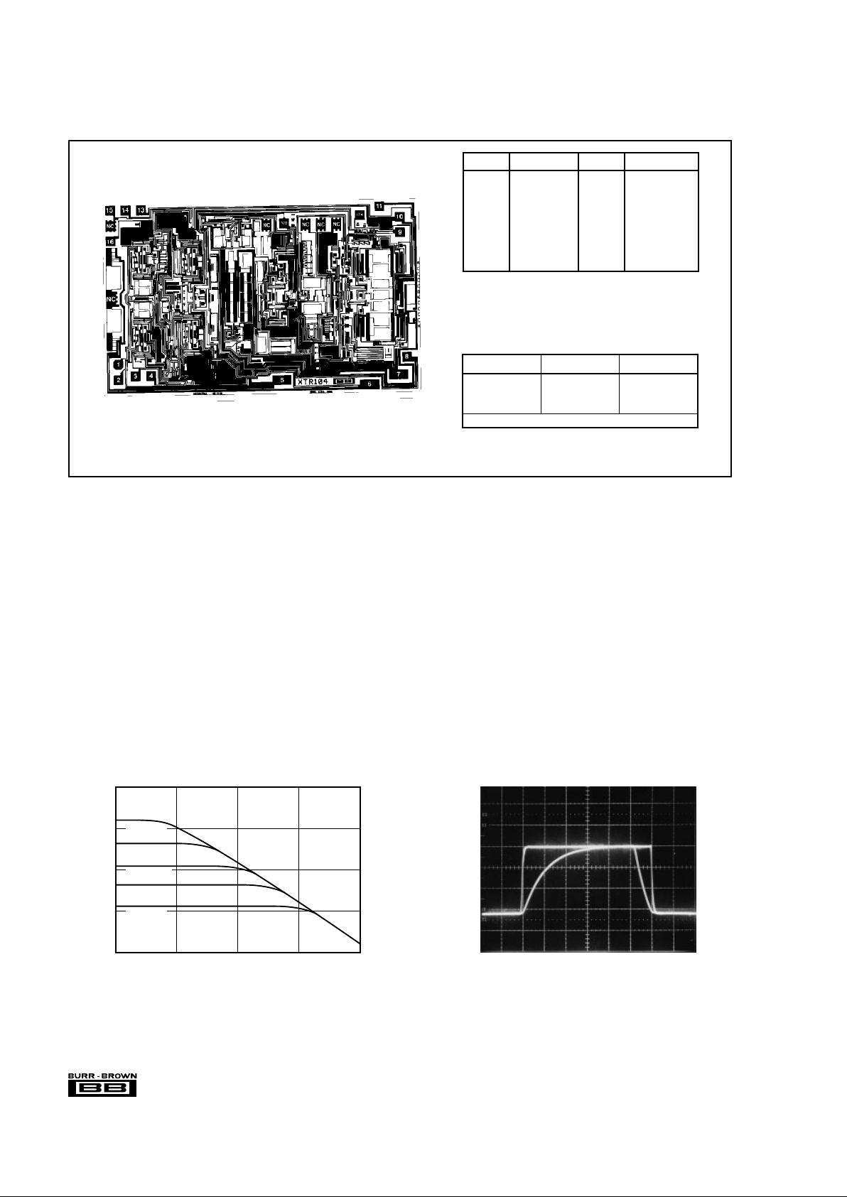
DICE INFORMATION
XTR104 DIE TOPOGRAPHY
PAD FUNCTION
9R
LIN
10 V+
11 E (Emitter)
12A, 12B V
REF
13 B (Base)
14 Zero Adj.
15 Zero Adj.
16 Zero Adj.
PAD FUNCTION
1V
+
IN
2V
–
IN
3V
+
LIN
4V
–
LIN
5R
G
6R
G
7I
O
8R
LIN
Pads 12A and 12B must be connected.
NC: No Connection
Substrate Bias: Internally connected to the I
O
terminal
(#7).
FPO
MECHANICAL INFORMATION
MILS (0.001") MILLIMETERS
Die Size 168 x 104 ±5 4.27 x 2.64 ±0.13
Die Thickness 20 ±3 0.51 ±0.08
Min. Pad Size 4 x 4 0.1 x 0.1
Backing None
TYPICAL PERFORMANCE CURVES
TA = +25°C, V+ = 24V, unless otherwise noted.
100 1k 10k 100k
0
Frequency (Hz)
TRANSCONDUCTANCE vs FREQUENCY
1M
80
60
40
20
Transconductance (20 Log mA/V)
RG = 25Ω
RG = 100Ω
R
G
= 400Ω
R
G
= 2kΩ
R
G
= ∞
4mA
20mA
RG = 25Ω
R
G
= ∞
STEP RESPONSE
100µs/Div
5mA/Div
 Loading...