

Burr Brown XTR103BU-1K, XTR103BU, XTR103BP, XTR103AU-1K, XTR103AU Datasheet
...
©
1992 Burr-Brown Corporation PDS-1145E Printed in U.S.A. October, 1993
International Airport Industrial Park • Mailing Address: PO Box 11400, Tucson, AZ 85734 • Street Address: 6730 S. Tucson Blvd., Tucson, AZ 85706 • Tel: (520) 746-1111 • Twx: 910-952-1111
Internet: http://www.burr-brown.com/ • FAXLine: (800) 548-6133 (US/Canada Only) • Cable: BBRCORP • Telex: 066-6491 • FAX: (520) 889-1510 • Immediate Product Info: (800) 548-6132
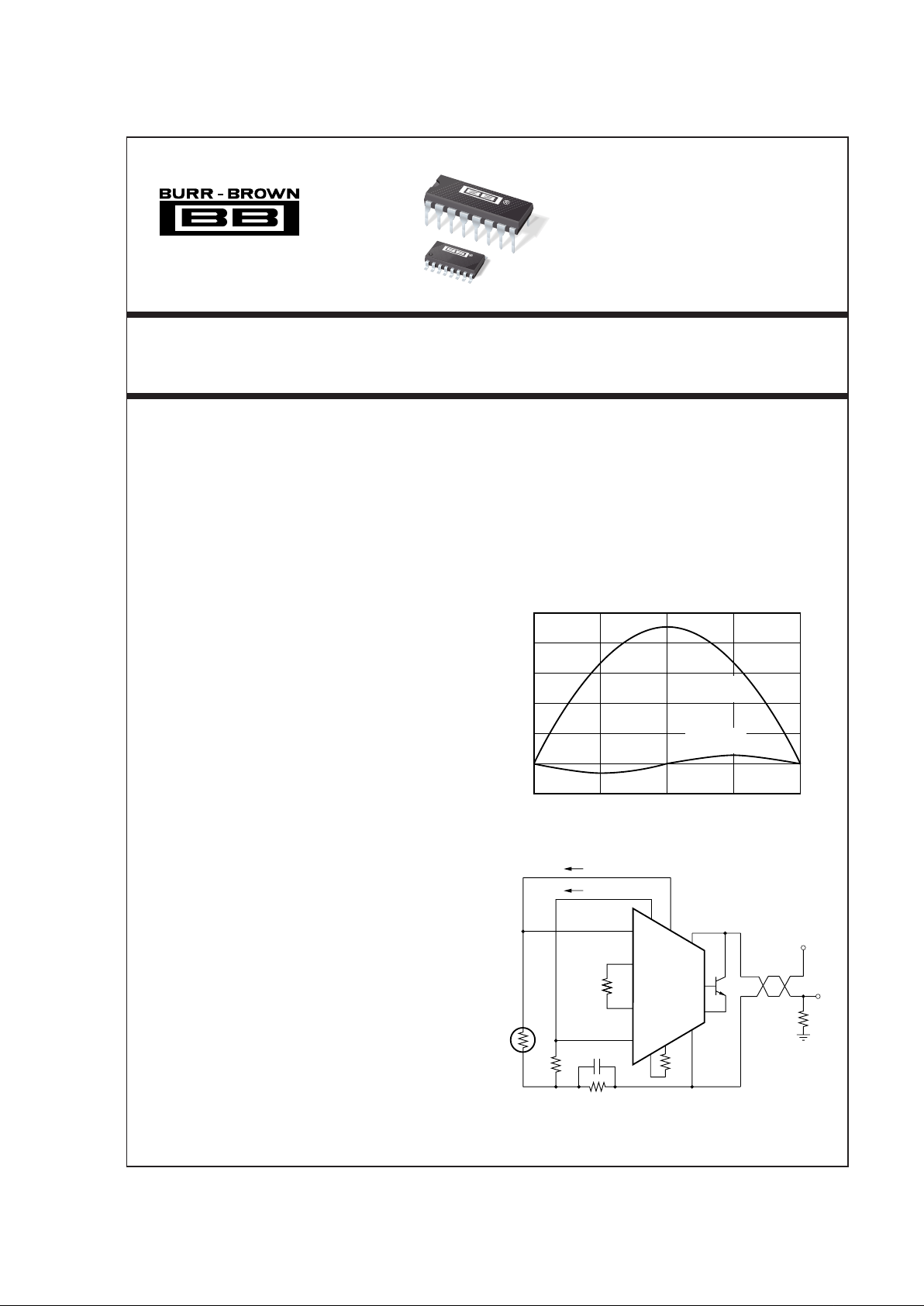
–200°C
Pt100 NONLINEARITY CORRECTION
USING XTR103
Process Temperature (°C)
+850°C
5
4
3
2
1
0
–1
Uncorrected
RTD Nonlinearity
Corrected
Nonlinearity
Nonlinearity (%)
XTR103
4-20mA Current Transmitter with
RTD EXCITATION AND LINEARIZATION
FEATURES
● LESS THAN ±1% TOTAL ADJUSTED
ERROR, –40
°C TO +85°C
● RTD EXCITATION AND LINEARIZATION
● TWO OR THREE-WIRE RTD OPERATION
● WIDE SUPPLY RANGE: 9V to 40V
● HIGH PSR: 110dB min
● HIGH CMR: 80dB min
APPLICATIONS
● INDUSTRIAL PROCESS CONTROL
● FACTORY AUTOMATION
● SCADA
DESCRIPTION
The XTR103 is a monolithic 4-20mA, two-wire
current transmitter designed for Platinum RTD temperature sensors. It provides complete RTD current
excitation, instrumentation amplifier, linearization, and
current output circuitry on a single integrated circuit.
Versatile linearization circuitry provides a 2nd-order
correction to the RTD, typically achieving a 40:1
improvement in linearity.
Instrumentation amplifier gain can be configured for a
wide range of temperature measurements. Total
adjusted error of the complete current transmitter,
including the linearized RTD is less than ±1% over the
full –40 to +85°C operating temperature range. This
includes zero drift, span drift and nonlinearity. The
XTR103 operates on loop power supply voltages down
to 9V.
The XTR103 is available in 16-pin plastic DIP and
SOL-16 surface-mount packages specified for the
–40°C to +85°C temperature range.
RTD
XTR103
–
R
L
4-20 mA
V
PS
+
9 to 40V
IR = 0.8mA
IR = 0.8mA
V
O
R
LIN
R
G
®
XTR103
XTR103
2
®
XTR103
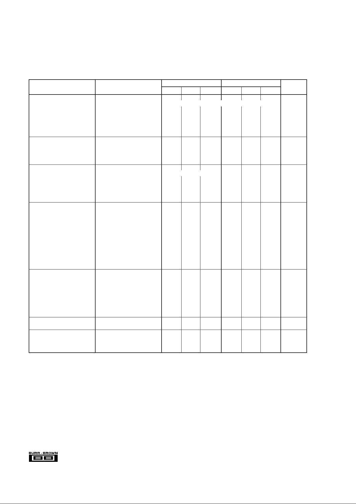
✻ Specification same as XTR103BP.
NOTES: (1) Includes corrected Pt100 nonlinearity for process measurement spans greater than 100°C, and over-temperature zero and span effects. Does not include
initial offset and gain errors which are normally trimmed to zero at 25°C. (2) Describes accuracy of the 4mA low-scale offset current. Does not include input amplifier
effects. Can be trimmed to zero. (3) Voltage measured with respect to I
O
pin. (4) Does not include TCR of gain-setting resistor, RG. (5) Measured with R
LIN
= ∞ to
disable linearization feature.
IO = VIN • (0.016 + 40/RG) + 4mA, VIN in Volts, RG in Ω
SPECIFICATIONS
ELECTRICAL
At TA = +25°C, V+ = 24V, and 2N6121 external transistor, unless otherwise noted.
XTR103BP/BU XTR103AP/AU
PARAMETER CONDITIONS MIN TYP MAX MIN TYP MAX UNITS
OUTPUT
Output Current Equation A
Total Adjusted Error
(1)
T
MIN
to T
MAX
±1 ±2 % of FS
Output Current, Specified Range 4 20 ✻✻mA
Over-Scale Limit 34 40 ✻✻ mA
Under Scale-Limit 3.6 3.8 ✻✻ mA
Full Scale Output Error V
IN
= 1V, RG = ∞±15 ±50 ✻ ±100 µA
Noise: 0.1Hz to 1kHz R
G
= 40Ω 8 ✻ µAp-p
ZERO OUTPUT
(2)
VIN = 0, RG = ∞ 4 ✻ mA
Initial Error ±5 ±50 ✻ ±100 µA
vs Temperature ±0.2 ±0.5 ✻ ±1 µA/°C
vs Supply Voltage, V+ V+ = 9V to 40V
(3)
0.5 2 ✻✻ µA/V
vs Common-Mode Voltage V
CM
= 2V to 4V
(3)
0.1 2 ✻✻ µA/V
SPAN
Span Equation (Transconductance) S = 0.016 + 40/R
G
✻ A/V
Untrimmed Error R
G
≥ 75Ω±0.1 ±1 ✻✻ %
vs Temperature
(4)
±20 ±50 ✻ ±100 ppm/°C
Nonlinearity: Ideal Input 0.01 ✻ %
RTD Input Pt100: –200°C to +850°C 0.1 ✻ %
R
LIN
= 1127Ω
INPUT
Differential Range R
G
= ∞ 1 ✻ V
Input Voltage Range
(3)
24✻✻V
Common-Mode Rejection V
IN
= 2V to 4V
(3)
80 100 ✻✻ dB
Impedance: Differential 3 ✻ GΩ
Common-Mode 0.5 ✻ GΩ
Offset Voltage ±0.5 ±2.5 ✻✻ mV
vs Temperature ±1 ±2.5 ±2 ±5 µV/°C
vs Supply Voltage, V+ V+ = 9V to 40V
(3)
110 130 ✻✻ dB
Input Bias Current 100 250 ✻✻ nA
vs Temperature 0.1 2 ✻✻ nA/°C
Input Offset Current 2 20 ✻✻ nA
vs Temperature 0.01 0.25 ✻✻ nA/°C
CURRENT SOURCES
(5)
Current 0.8 ✻ mA
Accuracy ±0.25 ±0.5 ✻ ±1%
vs Temperature ±25 ±50 ±50 ±100 ppm/°C
vs Power Supply, V+ V+ = 9V to 40V
(3)
50 ✻ ppm/V
Compliance Voltage
(3)
(V
–
IN
) – 0.2 (V+) – 5 ✻✻V
Matching ±0.5 ✻ %
vs Temperature ±10 ±25 ✻ ±50 ppm/°C
vs Power Supply, V+ V+ = 9V to 40V
(3)
10 ✻ ppm/V
POWER SUPPLY
Voltage Range
(3)
, V+ 9 40 ✻✻V
TEMPERATURE RANGE
Specification, T
MIN
to T
MAX
–40 85 ✻✻°C
Operating –40 125 ✻✻°C
θ
JA
80 ✻ °C/W
XTR1033
®
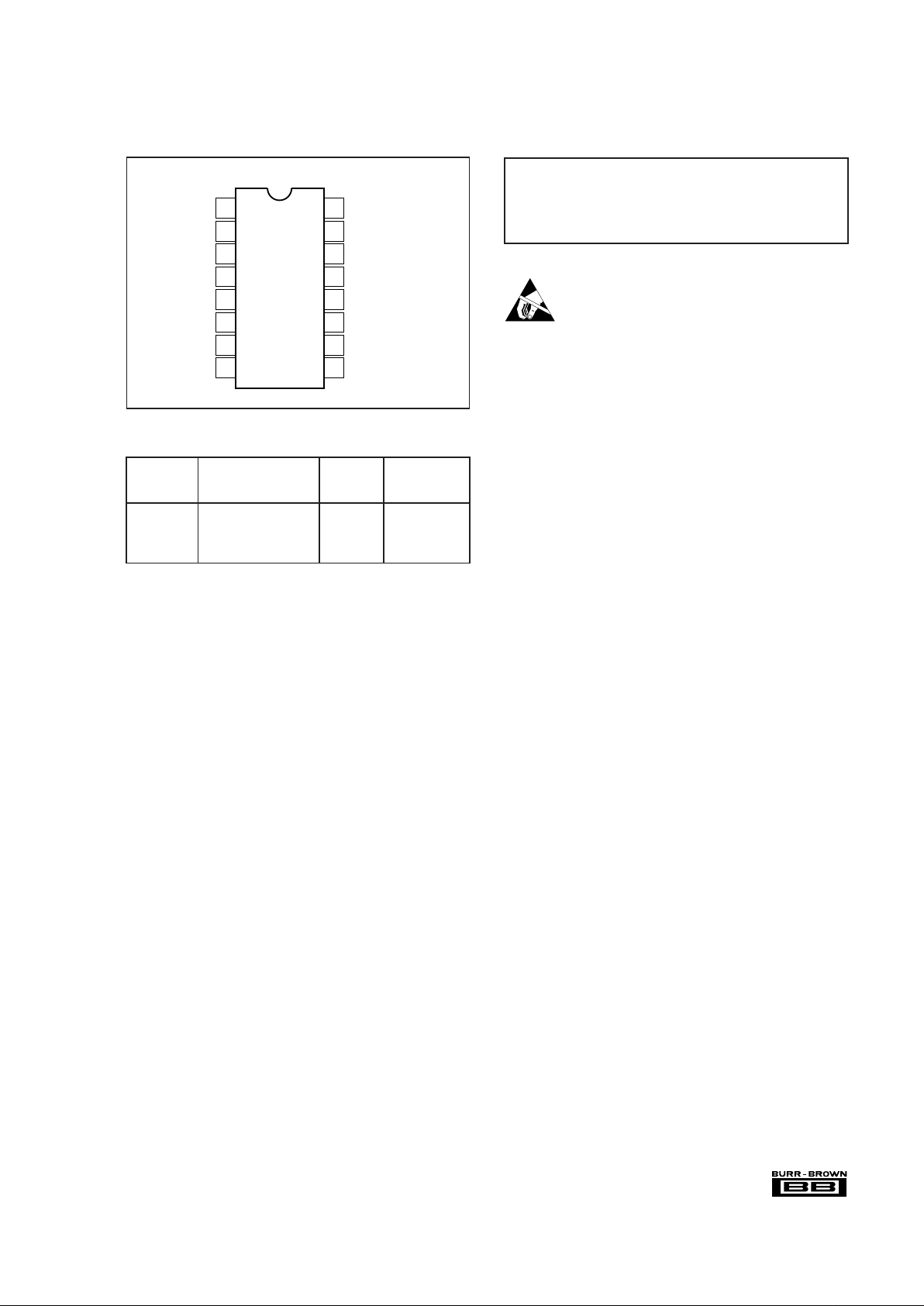
PIN CONFIGURATION
Power Supply, V+ (referenced to IO pin) .......................................... 40V
Input Voltage, V
+
IN
, V
–
IN
(referenced to IO pin) ........................ 0V to V+
Storage Temperature Range ........................................ –55°C to +125°C
Lead Temperature (soldering, 10s).............................................. +300°C
Output Current Limit ............................................................... Continuous
Junction Temperature ................................................................... +165°C
ABSOLUTE MAXIMUM RATINGS
Zero Adjust
Zero Adjust
V
IN
V
IN
R
G
R
G
I
O
R
LIN
Zero Adjust
B (Base)
E
INT
(Internal Emitter)
I
R2
I
R1
E (Emitter)
V+
R
LIN
1
2
3
4
5
6
7
8
16
15
14
13
12
11
10
9
–
+
ELECTROSTATIC
DISCHARGE SENSITIVITY
This integrated circuit can be damaged by ESD. Burr-Brown
recommends that all integrated circuits be handled with
appropriate precautions. Failure to observe proper handling
and installation procedures can cause damage.
ESD damage can range from subtle performance degradation
to complete device failure. Precision integrated circuits may
be more susceptible to damage because very small parametric
changes could cause the device not to meet its published
specifications.
TOP VIEW
The information provided herein is believed to be reliable; however, BURR-BROWN assumes no responsibility for inaccuracies or omissions. BURR-BROWN assumes
no responsibility for the use of this information, and all use of such information shall be entirely at the user’s own risk. Prices and specifications are subject to change
without notice. No patent rights or licenses to any of the circuits described herein are implied or granted to any third party. BURR-BROWN does not authorize or warrant
any BURR-BROWN product for use in life support devices and/or systems.
PACKAGE
DRAWING TEMPERATURE
PRODUCT PACKAGE NUMBER
(1)
RANGE
XTR103AP 16-pin Plastic DIP 180 –40°C to +85°C
XTR103BP 16-pin Plastic DIP 180 –40°C to +85°C
XTR103AU SOL-16 Surface Mount 211 –40°C to +85°C
XTR103BU SOL-16 Surface Mount 211 –40°C to +85°C
NOTE: (1) For detailed drawing and dimension table, please see end of data
sheet, or Appendix C of Burr-Brown IC Data Book.
PACKAGE/ORDERING INFORMATION
 Loading...