

Burr Brown XTR101BG, XTR101AU-1K, XTR101AU, XTR101AP, XTR101AG Datasheet
©
1986 Burr-Brown Corporation PDS-627G Printed in U.S.A. October, 1993
International Airport Industrial Park • Mailing Address: PO Box 11400, Tucson, AZ 85734 • Street Address: 6730 S. Tucson Blvd., Tucson, AZ 85706 • Tel: (520) 746-1111 • Twx: 910-952-1111
Internet: http://www.burr-brown.com/ • FAXLine: (800) 548-6133 (US/Canada Only) • Cable: BBRCORP • Telex: 066-6491 • FAX: (520) 889-1510 • Immediate Product Info: (800) 548-6132
XTR101
Precision, Low Drift
4-20mA TWO-WIRE TRANSMITTER
FEATURES
● INSTRUMENTATION AMPLIFIER INPUT
Low Offset Voltage, 30
µV max
Low Voltage Drift, 0.75
µV/°C max
Low Nonlinearity, 0.01% max
● TRUE TWO-WIRE OPERATION
Power and Signal on One Wire Pair
Current Mode Signal Transmission
High Noise Immunity
● DUAL MATCHED CURRENT SOURCES
● WIDE SUPPLY RANGE: 11.6V to 40V
● –40
°C to +85°C SPECIFICATION RANGE
● SMALL 14-PIN DIP PACKAGE, CERAMIC
AND PLASTIC
APPLICATIONS
● INDUSTRIAL PROCESS CONTROL
Pressure Transmitters
Temperature Transmitters
Millivolt Transmitters
● RESISTANCE BRIDGE INPUTS
● THERMOCOUPLE INPUTS
● RTD INPUTS
● CURRENT SHUNT (mV) INPUTS
● PRECISION DUAL CURRENT SOURCES
● AUTOMATED MANUFACTURING
● POWER/PLANT ENERGY SYSTEM
MONITORING
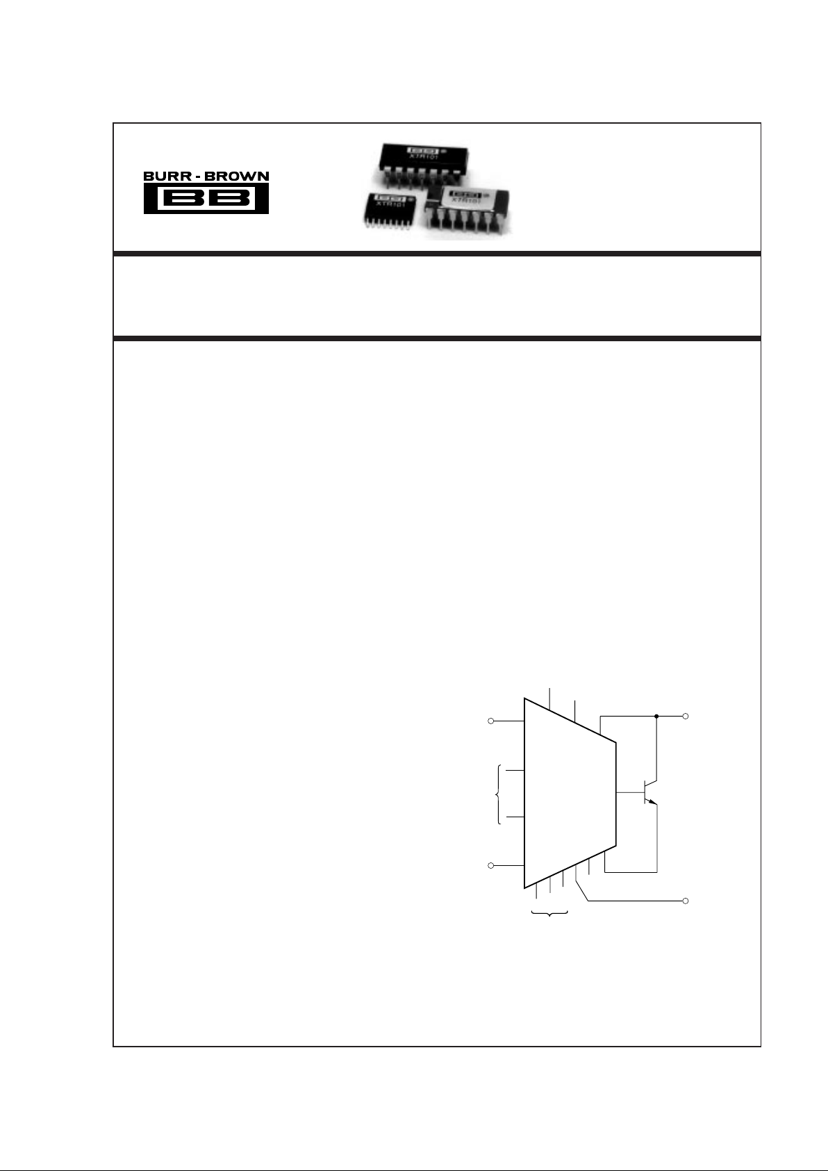
DESCRIPTION
The XTR101 is a microcircuit, 4-20mA, two-wire
transmitter containing a high accuracy instrumentation amplifier (IA), a voltage-controlled output current
source, and dual-matched precision current reference.
This combination is ideally suited for remote signal
conditioning of a wide variety of transducers such as
thermocouples, RTDs, thermistors, and strain gauge
bridges. State-of-the-art design and laser-trimming,
wide temperature range operation and small size make
it very suitable for industrial process control applications. In addition, the optional external transistor allows even higher precision.
The two-wire transmitter allows signal and power to
be supplied on a single wire-pair by modulating the
power supply current with the input signal source. The
transmitter is immune to voltage drops from long runs
and noise from motors, relays, actuators, switches,
transformers, and industrial equipment. It can be used
by OEMs producing transmitter modules or by data
acquisition system manufacturers.
2
B
14
9
1
8
11
10
3
5
6
4
XTR101
e
1
12
Optional
Offset Null
Optional
External
Transistor
REF1
I
REF2
I
I
OUT
7
13
E
(1)
(1)
e
2
Span
NOTE:
(1)
Pins 12 and 13 are used for optional BW control.
+
–
+V
CC
®
®
XTR101 2
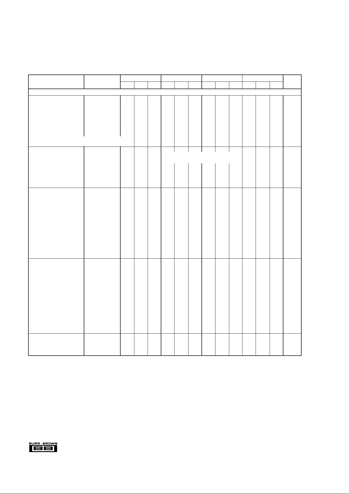
SPECIFICATIONS
ELECTRICAL
At TA = +25°C, +VCC = 24VDC, and RL = 100Ω with external transistor connected, unless otherwise noted
✻ Same as XTR101AG.
NOTES: (1) See Typical Performance Curves. (2) Span error shown is untrimmed and may be adjusted to zero. (3) e
1
and e2 are signals on the –In and +In terminals
with respect to the output, pin 7. While the maximum permissible ∆e is 1V, it is primarily intended for much lower input signal levels, e.g., 10mV or 50mV full scale
for the XTR101A and XTR101B grades respectively. 2mV FS is also possible with the B grade, but accuracy will degrade due to possible errors in the low value
span resistance and very high amplification of offset, drift, and noise. (4) Offset voltage is trimmed with the application of a 5V common-mode voltage. Thus the
associated common-mode error is removed. See Application Information section.
The information provided herein is believed to be reliable; however, BURR-BROWN assumes no responsibility for inaccuracies or omissions. BURR-BROWN assumes
no responsibility for the use of this information, and all use of such information shall be entirely at the user’s own risk. Prices and specifications are subject to change
without notice. No patent rights or licenses to any of the circuits described herein are implied or granted to any third party. BURR-BROWN does not authorize or warrant
any BURR-BROWN product for use in life support devices and/or systems.
XTR101AG XTR101BG XTR101AP XTR101AU
PARAMETER CONDITIONS MIN TYP MAX MIN TYP MAX MIN TYP MAX MIN TYP MAX UNITS
OUTPUT AND LOAD CHARACTERISTICS
Current Linear Operating Region 4 20
✻✻✻✻✻✻
mA
Derated Performance 3.8 22
✻✻✻✻✻✻
mA
Current Limit 28 38
✻✻
31
✻
31
✻
mA
Offset Current Error I
OS
, IO = 4mA ±3.9 ±10 ±2.5 ±6 ±8.5 ±19 ±8.5 ±19 µA
vs Temperature ∆I
OS
/∆T ±10.5 ±20 ±8 ±15 ±10.5 ±20
✻
ppm, FS/°C
Full Scale Output Current Error Full Scale = 20mA ±20 ±40 ±15 ±30 ±30 ±60 ±30 ±60 µA
Power Supply Voltage V
CC
, Pins 7 and 8, +11.6 ±40
✻✻✻✻✻✻
VDC
Compliance
(1)
Load Resistance At VCC = +24V, IO = 20mA 600
✻
600
✻
Ω
At V
CC
= +40V, IO = 20mA 1400
✻
1400
✻
Ω
SPAN
Output Current Equation R
S
in Ω, e1 and e2 in V iO = 4mA + [0.016Ω + (40/RS)] (e2 – e1)
Span Equation R
S
in Ω S = [0.016Ω + (40/RS)] A/V
vs Temperature Excluding TCR of R
S
±30 ±100
✻✻ ✻✻ ✻✻
ppm/°C
Untrimmed Error
(2)
ε
SPAN
–5 –2.5 0
✻✻✻✻✻✻✻✻✻
%
Nonlinearity
ε
NONLINEARITY
0.01
✻✻✻
%
Hysteresis 0
✻✻✻
%
Dead Band 0
✻✻✻
%
INPUT CHARACTERISTICS
Impedance: Differential 0.4 || 3
✻✻✻
GΩ || pF
Common-Mode 10 || 3
✻✻✻
GΩ || pF
Voltage Range, Full Scale ∆e = (e
2
– e1)
(3)
01
✻✻✻✻✻✻
V
Offset Voltage V
OS
±30 ±60 ±20 ±30
✻
±100
✻
±100 µV
vs Temperature ∆V
OS
/∆T ±0.75 ±1.5 ±0.35 ±0.75
✻✻ ✻✻
µV/°C
Power Supply Rejection ∆V
CC
/PSRR = VOS Error 110 125
✻✻ ✻
122 110 122 dB
Bias Current I
B
60 150
✻✻ ✻✻ ✻✻
nA
vs Temperature ∆I
B
/∆T 0.30 1
✻✻ ✻✻ ✻✻
nA/°C
Offset Current I
OSI
10 ±30
✻
±20
✻✻ ✻✻
nA
vs Temperature ∆ I
OSI
/∆T 0.1 0.3
✻✻ ✻✻ ✻✻
nA/°C
Common-Mode Rejection
(4)
DC 90 100
✻✻ ✻✻ ✻✻
dB
Common-Mode Range e
1
and e2 with Respect
to Pin 7 4 6
✻✻✻✻✻✻
V
CURRENT SOURCES
Magnitude 1
✻✻✻
mA
Accuracy V
CC
= 24V,
V
PIN 8
– V
PIN 10,11
= 19V
R
2
= 5kΩ, Fig. 5 ±0.06 ±0.17 ±0.025 ±0.075 ±0.2 ±0.37 ±0.2 ±0.37 %
vs Temperature ±50 ±80 ±30 ±50
✻✻ ✻✻
ppm/°C
vs V
CC
±3
✻✻✻
ppm/V
vs Time ±8
✻✻✻
ppm/month
Compliance Voltage With Respect to Pin 7 0
V
CC
– 3.5
✻✻✻✻✻✻
V
Ratio Match Tracking
Accuracy (1 – I
REF1/IREF2
) X 100% ±0.014 ±0.06 ± 0.009 ±0.04 ±0.031 ±0.088 ±0.031 ±0.088 %
vs Tempeature ±15 10
✻✻
ppm/°C
vs V
CC
±10
✻✻✻
ppm/V
vs Time ±1
✻✻✻
ppm/month
Output Impedance 10 20
✻✻ ✻
15
✻
15 MΩ
TEMPERATURE RANGE
Specification –40 +85
✻✻
–40 +85
✻✻
°C
Operating –55 +125
✻✻
–40 +85 –40 +85 °C
Storage –55 +165
✻✻
–55 +125 –55 +125 °C

®
XTR101
3
PIN CONFIGURATION
Top View DIP Top View SOIC
Zero Adjust
Zero Adjust
–In
+In
Span
Span
Out
NC
Zero Adjust
Bandwidth
B Control
I
REF2
I
REF1
E
+V
CC
NC
1
2
3
4
5
6
7
8
16
15
14
13
12
11
10
9
SOL-16
Surface-Mount
Zero Adjust
Zero Adjust
–In
+In
Span
Span
Out
Zero Adjust
Bandwidth
B Control
I
REF2
I
REF1
E
+V
CC
1
2
3
4
5
6
7
14
13
12
11
10
9
8
DIP
PACKAGE
DRAWING TEMPERATURE
PRODUCT PACKAGE NUMBER
(1)
RANGE
XTR101AG 14-Pin Ceramic DIP 169 –40°C to +85°C
XTR101BG 14-Pin Ceramic DIP 169 –40°C to +85°C
XTR101AP 14-Pin Plastic DIP 010 –40°C to +85°C
XTR101AU 16-Lead SOIC 211 –40°C to +85°C
NOTE: (1) For detailed drawing and dimension table, please see end of data
sheet, or Appendix C of Burr-Brown IC Data Book.
ABSOLUTE MAXIMUM RATINGS
Power Supply, +VCC...........................................................................40V
Input Voltage, e
1
or e2........................................................ ≥V
OUT
, ≤+V
CC
Storage Temperature Range, Ceramic ........................ –55°C to +165°C
Plastic ............. –55°C to +125°C
Lead Temperature (soldering 10s) G, P ...................................... +300°C
(wave soldering, 3s) U .......................... +260°C
Output Short-Circuit Duration ........................... Continuous +V
CC
to I
OUT
Junction Temperature ................................................................... +165°C
PACKAGE/ORDERING INFORMATION
ELECTROSTATIC
DISCHARGE SENSITIVITY
This integrated circuit can be damaged by ESD. Burr-Brown
recommends that all integrated circuits be handled with
appropriate precautions. Failure to observe proper handling
and installation procedures can cause damage.
ESD damage can range from subtle performance degradation to complete device failure. Precision integrated circuits
may be more susceptible to damage because very small
parametric changes could cause the device not to meet its
published specifications.
®
XTR101 4
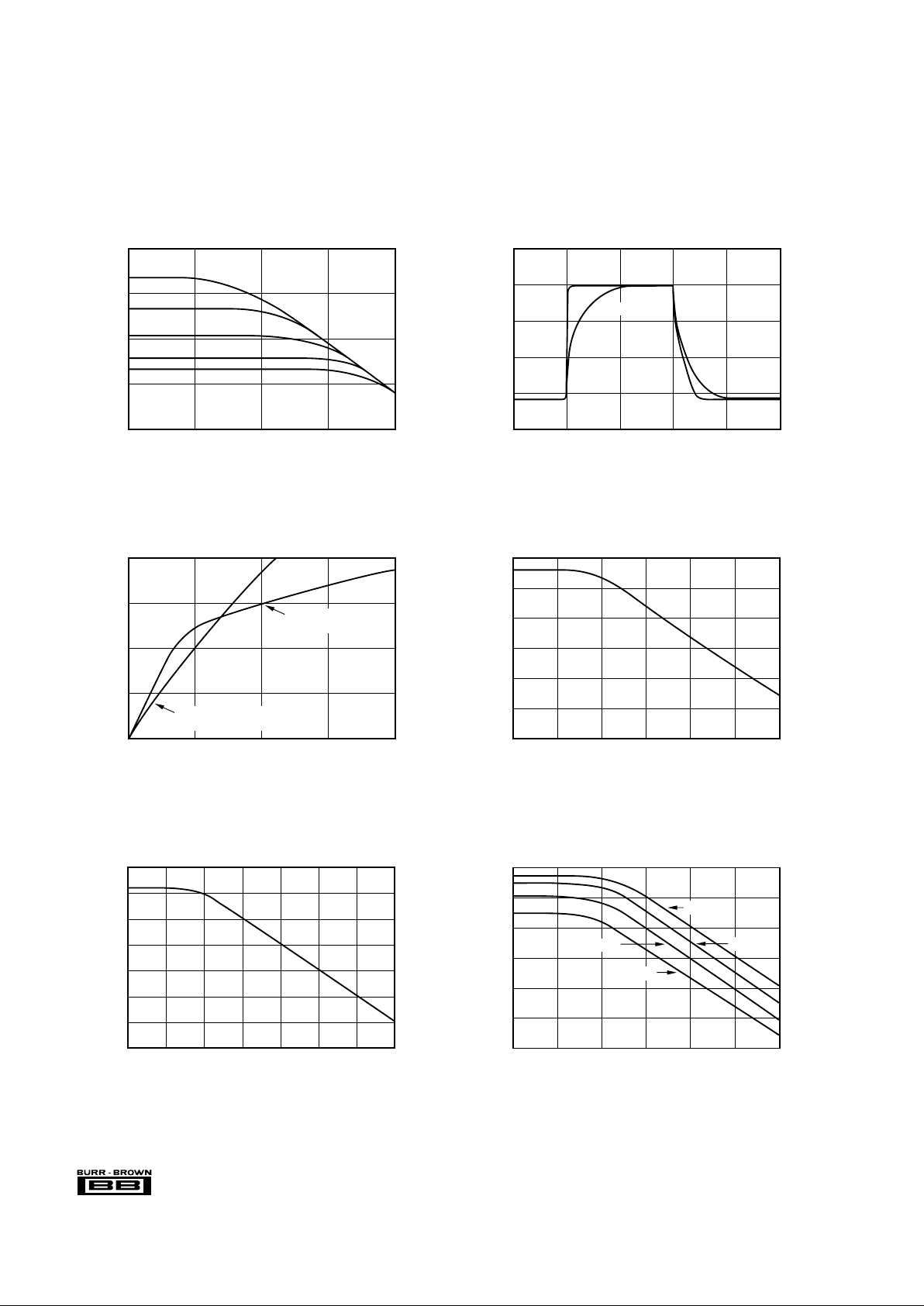
TYPICAL PERFORMANCE CURVES
At TA = +25°C, +VCC = 24VDC, unless otherwise noted.
100 1k 10k 100k
0
Frequency (Hz)
SPAN vs FREQUENCY
1M
80
60
40
20
Transconductance (20 Log m )
Ω
RS = 25Ω
R
S
= 100Ω
R
S
= 400Ω
R
S
= 2kΩ
R
S
= ∞
C
C
= 0
0
Time (µs)
STEP RESPONSE
25
20
15
10
5
Output Current (mA)
0 200 400 600 800 1000
RS = 25Ω
R
S
= ∞
0 100 200 300
0
R
S
(Ω)
FULL SCALE INPUT VOLTAGE vs R
S
400
0.08
0.06
0.04
0.02
∆e
IN
Full Scale (V)
0 to 800mV and
0 to 8kΩ scale
0
0.8
0.6
0.4
0.2
∆e
IN
Full Scale (V)
02468
R
S
(kΩ)
0 to 80mV (low level signals)
and 0 to 400Ω scale
0
0.1 1 10 100 1k 10k
Frequency (Hz)
CMR (dB)
COMMON-MODE REJECTION vs FREQUENCY
100k
120
100
80
60
40
20
120
100
80
60
40
20
0.1
0
Frequency (Hz)
Power Supply Rejection (dB)
POWER SUPPLY REJECTION vs FREQUENCY
140
10 100 1k 100k 1M 10M10k
0.1
1 10 100 1k 10k 100k
Bandwidth Control, C
C
(pF)
Bandwidth (Hz)
BANDWIDTH vs PHASE COMPENSATION
1M
100k
10k
1k
100
10
1
RS = 25Ω
R
S
= 100Ω
R
S
= 400Ω
R
S
= ∞
®
XTR101
5
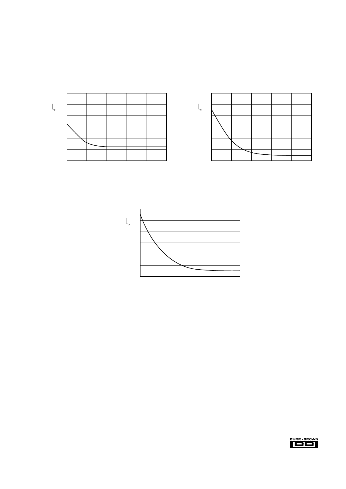
TYPICAL PERFORMANCE CURVES (CONT)
At TA = +25°C, +V
CC
= 24VDC, unless otherwise noted.
10
1 10 100 1k 10k
0
Frequency (Hz)
INPUT VOLTAGE NOISE DENSITY vs FREQUENCY
100k
60
50
40
30
20
Input Noise Voltage (nV/ Hz )
0
Frequency (Hz)
INPUT CURRENT NOISE DENSITY vs FREQUENCY
6
5
4
3
2
1
Input Noise Current (pA/ Hz )
1 10 100 1k 10k 100k
0
Frequency (Hz)
OUTPUT CURRENT NOISE DENSITY vs FREQUENCY
6
5
4
3
2
1
Output Noise Current (nA/ Hz )
1 10 100 1k 10k 100k
THEORY OF OPERATION
A simplified schematic of the XTR101 is shown in Figure 1.
Basically the amplifiers, A
1
and A2, act as a single power
supply instrumentation amplifier controlling a current source,
A3 and Q1. Operation is determined by an internal feedback
loop. e
1
applied to pin 3 will also appear at pin 5 and
similarly e
2
will appear at pin 6. Therefore the current in RS,
the span setting resistor, will be I
S
= (e2 – e1)/RS = eIN/RS.
This current combines with the current, I
3
, to form I1. The
circuit is configured such that I
2
is 19 times I1. From this
point the derivation of the transfer function is straightforward but lengthy. The result is shown in Figure 1.
Examination of the transfer function shows that I
O
has a
lower range-limit of 4mA when e
IN
= e2 – e1 = 0V. This 4mA
is composed of 2mA quiescent current exiting pin 7 plus
2mA from the current sources. The upper range limit of IO is
set to 20mA by the proper selection of R
S
based on the upper
range limit of e
IN
. Specifically RS is chosen for a 16mA
output current span for the given full scale input voltage
span; i.e., (0.016 + 40/RS)(eIN full scale) = 16mA. Note that
Ω
since IO is unipolar e2 must be kept larger than e1; i.e., e2 ≥
e
1
or eIN ≥ 0. Also note that in order not to exceed the output
upper range limit of 20mA, e
IN
must be kept less than 1V
when R
S
= ∞ and proportionately less as RS is reduced.
INSTALLATION AND
OPERATING INSTRUCTIONS
BASIC CONNECTION
The basic connection of the XTR101 is shown in Figure 1.
A difference voltage applied between input pins 3 and 4 will
cause a current of 4-20mA to circulate in the two-wire
output loop (through R
L
, VPS, and D1). For applications
requiring moderate accuracy, the XTR101 operates very
cost-effectively with just its internal drive transistor. For
more demanding applications (high accuracy in high gain)
an external NPN transistor can be added in parallel with the
internal one. This keeps the heat out of the XTR101 package
 Loading...