

Burr Brown VSP3100Y-2K, VSP3100Y Datasheet
14-Bit, 10MHz
CCD/CIS SIGNAL PROCESSOR
®
VSP3100
DESCRIPTION
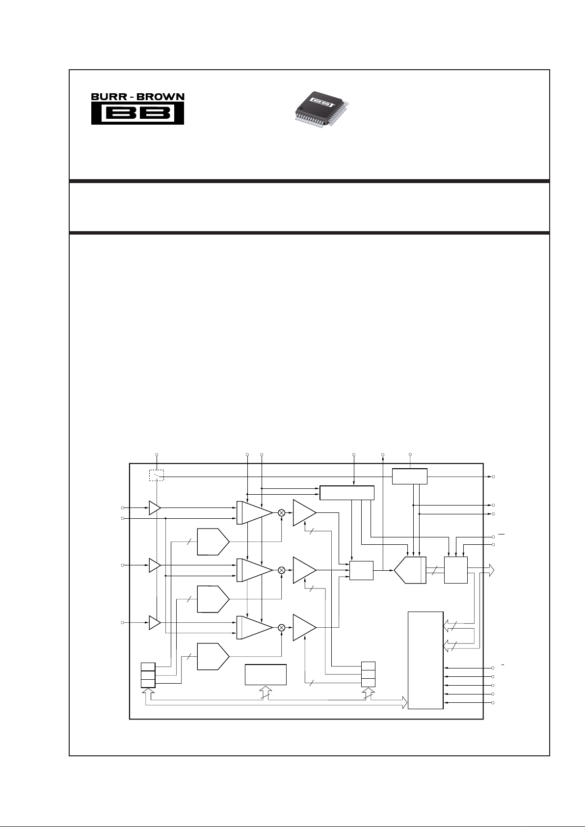
The VSP3100 is a complete CCD/CIS image processor which operates from a single +5V supply.
This complete image processor includes three Correlated Double Samplers (CDS) and Programmable Gain
Amplifiers (PGA) to process CCD signals.
These three channel inputs also allow Contact Image
Sensor (CIS) inputs.
The VSP3100 is an interface compatible with the
VSP3000 which is 12-bit one-chip product.
The VSP3100 can be operated from 0°C to +85°C and
is available in an LQFP-48 package.
FEATURES
● INTEGRATED TRIPLE-CORRELATED
DOUBLE SAMPLER
● OPERATION MODE SELECTABLE:
1-Channel, 3-Channel, 10MSPS (typ),
CCD/CIS Mode
● PROGRAMMABLE GAIN AMPLIFIER:
0dB to +13dB
● SELECTABLE OUTPUT MODES:
Normal/Demultiplexed
● OFFSET CONTROL RANGE: ±400mV
● +3V, +5V Digital Output
● LOW POWER: 450mW (typ)
● LQFP-48 SURFACE-MOUNT PACKAGE
© 2000 Burr-Brown Corporation PDS-1583A Printed in U.S.A. April, 2000
International Airport Industrial Park • Mailing Address: PO Box 11400, Tucson, AZ 85734 • Street Address: 6730 S. Tucson Blvd., Tucson, AZ 85706 • Tel: (520) 746-1111
Twx: 910-952-1111 • Internet: http://www.burr-brown.com/ • Cable: BBRCORP • Telex: 066-6491 • FAX: (520) 889-1510 • Immediate Product Info: (800) 548-6132
For most current data sheet and other product
information, visit www.burr-brown.com
10
5
RINP
INN
Clamp
10
5
GINP
Clamp
10
5
58
3
10
14
CDS
CDS
CDS
PGA
PGA
PGA
BINP
Clamp
10-Bit
DAC
10-Bit
DAC
10-Bit
DAC
MUX
Timing Generator
Reference
Circuit
Digital
Output
Control
R
G
B
Offset
Register
R
G
B
Gain
Control
Register
Configuration
Register
Register
Port
14-Bit
A/D
P/S
WRT
RD
SCLK
SD
CM
REFP
REFN
V
DRV
B0-B13
(A0-A2, D0-D9)
OE
VSP3100
CK1CLP CK2
ADCCK
V
REF
TP0
VSP3100

2
®
VSP3100
SPECIFICATIONS
At TA = full specified temperature range, VCC = +5V, f
ADCCK
= 6MHz, f
CK1
= 2MHz, f
CK2
= 2MHz, PGA gain = 1, normal output mode, no output load, unless otherwise
specified.
VSP3100Y
PARAMETER CONDITIONS MIN TYP MAX UNITS
RESOLUTION 14 Bits
CONVERSION CHARACTERISTICS
1-, 3-Channel CDS Mode 10 MSPS
1-, 3-Channel CIS Mode 10 MSPS
DIGITAL INPUTS
Logic Family CMOS
Convert Command Start Conversion Rising Edge of ADCCK Clock
High Level Input Current (V
IN
= VCC) 20 µA
Low Level Input Current (VIN = 0V) 20 µA
Positive-Going Threshold Voltage Pins 18, 19, 20, 21, 22, 24 3.80 V
Negative-Going Threshold Voltage Pins 18, 19, 20, 21, 22, 24 1.25 V
Positive-Going Threshold Voltage Pins 12, 14, 15, 16 2.20 V
Negative-Going Threshold Voltage Pins 12, 14, 15, 16 0.80 V
Input Capacitance 5pF
ANALOG INPUTS
Full-Scale Input Range 0.5 3.5 Vp-p
Input Capacitance 10 pF
Input Limits AGND – 0.3 V
CC
+ 0.3 V
External Reference Voltage Range 0.25 0.3 V
Reference Input Resistance 800 Ω
DYNAMIC CHARACTERISTICS
Integral Non-Linearity (INL) ±4.0 LSB
Differential Non-Linearity (DNL) 0.5 LSB
No Missing Codes Guaranteed Bits
Output Noise Gain = 0dB, Input Grounded 0.5 LSBs rms
PSRR 0.04 % FSR
DC ACCURACY
Zero Error Gain = 0dB 0.8 % FS
Gain Error Gain = 0dB 1.5 % FS
DIGITAL OUTPUTS
Logic Family TTL/HCT
Logic Coding Straight Offset Binary
Digital Data Output Rate, Max Normal Mode 10 MHz
Demultiplexed Mode 10 MHz
V
DRV
Supply Range +2.7 +5.3 V
Output Voltage, V
DRV
= +5V
Low Level IOL = 50µA +0.1 V
High Level IOH = 50µA +4.6 V
Low Level I
OL
= 1.6mA +0.4 V
High Level IOH = 0.5mA +2.4 V
Output Voltage, V
DRV
= +3
Low Level I
OL
= 50µA +0.1 V
High Level IOH = 50µA +2.5 V
Ouput Enable Time Output Enable = LOW 20 40 ns
3-State Enable Time Output Enable = HIGH 2 10 ns
Output Capacitance 5pF
Data Latency 7 Clock Cycles
Data Output Delay C
L
= 15pF 12 ns
POWER SUPPLY REQUIREMENTS
Supply Voltage: V
CC
4.7 5 5.3 V
Supply Current: ICC (No Load) 3-Ch Mode 90 mA
1-Ch Mode 75 mA
Power Dissipation (No Load) 3-Ch Mode 450 mW
1-Ch Mode 375 mW
Thermal Resistance,
θ
JA
100 °C/W
SPECIFIED TEMPERATURE RANGE 0 to +85 °C
NOTE: (1) SNR = 20log (full-scale voltage/rms noise).
3
®
VSP3100
The information provided herein is believed to be reliable; however, BURR-BROWN assumes no responsibility for inaccuracies or omissions. BURR-BROWN
assumes no responsibility for the use of this information, and all use of such information shall be entirely at the user’s own risk. Prices and specifications are subject
to change without notice. No patent rights or licenses to any of the circuits described herein are implied or granted to any third party. BURR-BROWN does not
authorize or warrant any BURR-BROWN product for use in life support devices and/or systems.
Supply Voltage
(2)
.............................................................................................................. +6.5V
Supply Voltage Differences
(3)
................................................................................... ±0.1V
GND Voltage Differences
(4)
........................................................................................ ±0.1V
Digital Input Voltage................................................. –0.3V to (V
CC
+ 0.3V)
Analog Input Voltage................................................ –0.3V to (V
CC
+ 0.3V)
Input Current (any pins except suppplies) ...................................... ±10mA
Operating Temperature ........................................................ 0°C to +85°C
Storage Temperature...................................................... –55°C to +150°C
Junction Temperature .................................................................... +150°C
Lead Temperature (soldering) ....................................................... +150°C
Package Temperature (IR Reflow, peak, 10s)............................... +260°C
Package Temperature (IR Reflow, peak, 5s) ................................. +235°C
NOTES: (1) Stresses above these ratings may cause permanent damage.
Exposure to absolute maximum conditions for extended periods may degrade
device reliability. These are stress ratings only, and functional operation of the
device at these or any other conditions beyond those specified is not implied.
(2) V
CC, VDRV
. (3) Among VCC. (4) Among AGND.
ABSOLUTE MAXIMUM RATINGS
(1)
ELECTROSTATIC
DISCHARGE SENSITIVITY
This integrated circuit can be damaged by ESD. Burr-Brown
recommends that all integrated circuits be handled with
appropriate precautions. Failure to observe proper handling
and installation procedures can cause damage.
ESD damage can range from subtle performance degradation
to complete device failure. Precision integrated circuits may
be more susceptible to damage because very small parametric
changes could cause the device not to meet its published
specifications.
PRODUCT PACKAGE
VSP3100Y DEM-VSP3100Y
DEMO BOARD ORDERING INFORMATION
PACKAGE SPECIFIED
DRAWING TEMPERATURE PACKAGE ORDERING TRANSPORT
PRODUCT PACKAGE NUMBER RANGE MARKING NUMBER
(1)
MEDIA
VSP3100Y LQFP-48 340 0°C to +85°C VSP3100Y VSP3100Y 250-Piece Tray
""""VSP3100Y VSP3100Y/2K Tape and Reel
NOTE: (1) Models with a slash (/) are available only in Tape and Reel in the quantities indicated (e.g., /2K indicates 2000 devices per reel). Ordering 2000 pieces of
“VSP3100Y/2K” will get a single 2000-piece Tape and Reel.
PACKAGE/ORDERING INFORMATION
4
®
VSP3100
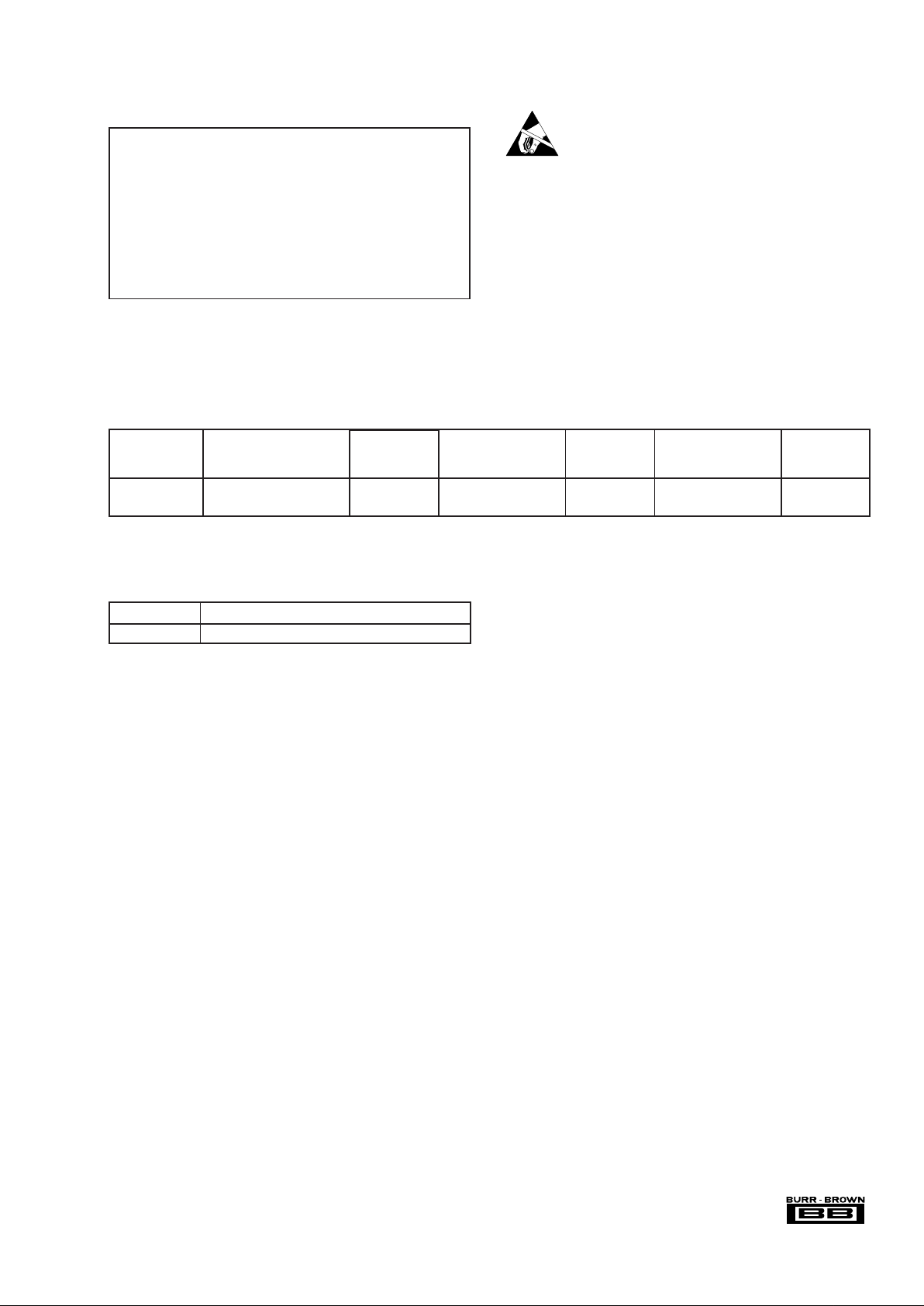
Top View LQFP
PIN DESCRIPTIONS
PIN DESIGNATOR TYPE DESCRIPTION PIN DESIGNATOR TYPE DESCRIPTION
1 CM AO Common-Mode Voltage
2 REFP AO Top Reference
3 AGND P Analog Ground
4 INN AI Red/Green/Blue Channel Reference Input
5 RINP AI Red Channel Analog Input
6 AGND P Analog Ground
7 GINP AI Green Channel Analog Input
8 AGND P Analog Ground
9 BINP AI Blue Channel Analog Input
10 AGND P Analog Ground
11 V
CC
P Analog Power Supply, +5V
12 CLP DI Clamp Enable:
“High” = Enable, “Low” = Disable
13 V
CC
P Analog Power Supply, +5V
14 ADCCK DI Clock for A/D Converter Digital Data Output
15 CK1 DI Sample Reference Clock
16 CK2 DI Sample Data Clock
17 AGND P Analog Ground
18 RD DI Read Signal for Registers
19 WRT DI Write Signal for Registers
20 P/S DI Parallel/Serial Port Select
“High” = Parallel Port, “Low” = Serial Port
21 SD DI Serial Data Input
22 SCLK DI Serial Data Shift Clock
23 V
CC
P Analog Power Supply, +5V
24 OE DI Output Enable
PIN CONFIGURATION
25 B0 (D0) LSB DIO A/D Output (Bit 0) and Register Data (Bit 0)
26 B1 (D1) DIO A/D Output (Bit 1) and Register Data (Bit 1)
27 B2 (D2) DIO A/D Output (Bit 2) and Register Data (Bit 2)
28 B3 (D3) DIO A/D Output (Bit 3) and Register Data (Bit 3)
29 B4 (D4) DIO A/D Output (Bit 4) and Register Data (Bit 4)
30 B5 (D5) DIO A/D Output (Bit 5) and Register Data (Bit 5)
31 B6 (D6) DIO A/D Output (Bit 6) and Register Data (Bit 6)
32 B7 (D7) DIO A/D Output (Bit 7) and Register Data (Bit 7)
33 B8 (D8) DIO A/D Output (Bit 8) and Register Data (Bit 8)
B0: Demiltiplexed Mode A/D Output (Bit 0) when Demultiplexed Output Mode
34 B9 (D9) DIO A/D Output (Bit 9) and Register Data (Bit 9)
B1: Demiltiplexed Mode A/D Output (Bit 1) when Demultiplexed Output Mode
35 B10 (A0) DIO A/D Output (Bit 10) and Register Address (Bit 0)
B2: Demiltiplexed Mode A/D Output (Bit 2) when Demultiplexed Output Mode
36 B11 (A1) DIO A/D Output (Bit 11) and Register Address (Bit 1)
B3: Demiltiplexed Mode A/D Output (Bit 3) when Demultiplexed Output Mode
37 B12 (A2) DIO A/D Output (Bit 12) and Register Address (Bit 2)
B4: Demiltiplexed Mode A/D Output (Bit 4) when Demultiplexed Output Mode
38 B13 MSB DO A/D Output (Bit 13)
B5: Demiltiplexed Mode A/D Output (Bit 5) when Demultiplexed Output Mode
39 AGND P Analog Ground
40 AGND P Analog Ground
41 V
DRV
P Digital Output Driver Power Supply
42 V
CC
P Analog Power Supply, +5V
43 V
CC
P Analog Power Supply, +5V
44 AGND P Analog Ground
45 TP0 AO A/D Converter Input Monitor Pin (single-ended output)
46 V
REF
AIO Reference Voltage Input/Output
47 V
CC
P Analog Power Supply, +5V
48 REFN AO Bottom Reference
36
35
34
33
32
31
30
29
28
27
26
25
B11 (A1)
B10 (A0)
B9 (D9)
B8 (D8)
B7 (D7)
B6 (D6)
B5 (D5)
B4 (D4)
B3 (D3)
B2 (D2)
B1 (D1)
B0 (D0) LSB
REFN
VCCV
REF
TP0
AGND
VCCVCCV
DRV
AGND
AGND
B13 MSB
B12 (A2)
V
CC
ADCCK
CK1
CK2
AGND
RD
WRT
P/S
SD
SCLK
V
CC
OE
1
2
3
4
5
6
7
8
9
10
11
12
CM
REFP
AGND
INN
RINP
AGND
GINP
AGND
BINP
AGND
V
CC
CLP
48 47 46 45 44 43 42
41 40 39 38
13 14 15 16 17 18 19 20 21 22 233724
VSP3100Y
5
®
VSP3100
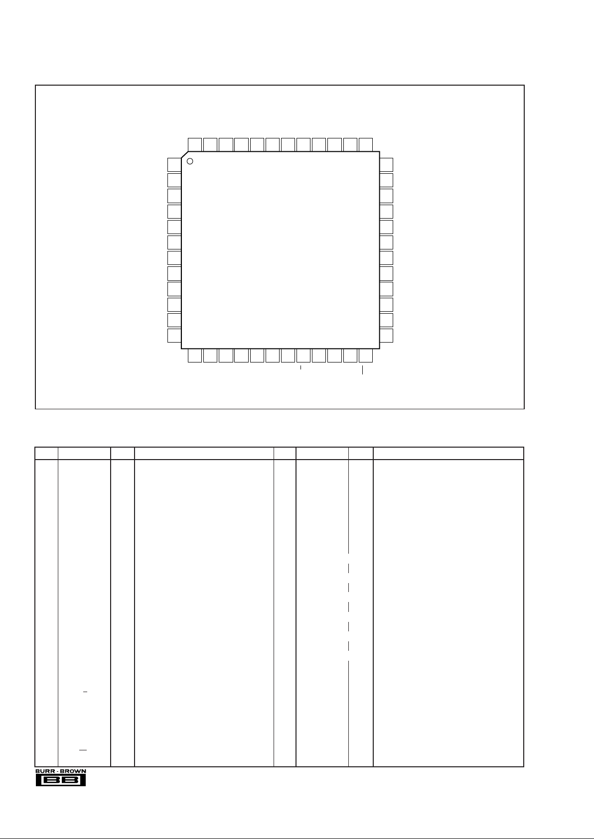
TIMING DIAGRAMS
Timing Specifications: VCC = +5V supply and normal output mode with the specified temperature range, unless otherwise noted.
SYMBOL PARAMETER MIN TYP MAX UNITS
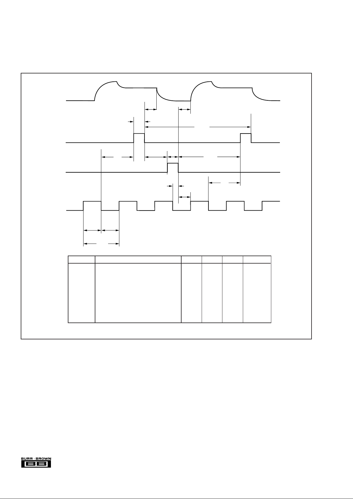
t
CK1W-1
CK1 Pulse Width 20 40 ns
t
CK1P-1
1-Channel Mode Conversion Rate 100 166 ns
t
CK2W-1
CK2 Pulse Width 20 40 ns
t
CK1CK2-1
CK1 Falling to CK2 Rising 15 ns
t
CK2CK1-1
CK2 Falling to CK1 Rising 40 ns
t
CK1ADC
CK1 Rising to ADCCK Falling 20 ns
t
ADCCK2-1
ADCCK Falling to CK2 Falling 15 ns
t
ADCW
ADCCK Pulse Width 41 83 ns
t
ADCP
ADCCK Period 83 166 ns
t
S
Sampling Delay 10 ns
t
SET
ADCCK Rising to CK1 Rising 10 ns
t
CNV
Conversion Delay 40 ns
1-Channel CCD Mode Timing
CCD Output
CK1
CK2
ADCCK
t
S
t
S
t
CK1P-1
t
SET
t
CK1ADC
t
ADCCK2-1
t
CK1CK2-1
t
CK2CK1-1
t
CK2W-1
t
CNV
t
ADCW
t
ADCP
t
ADCW
t
CK1W-1
Pixel 1
Pixel 1
Pixel 2
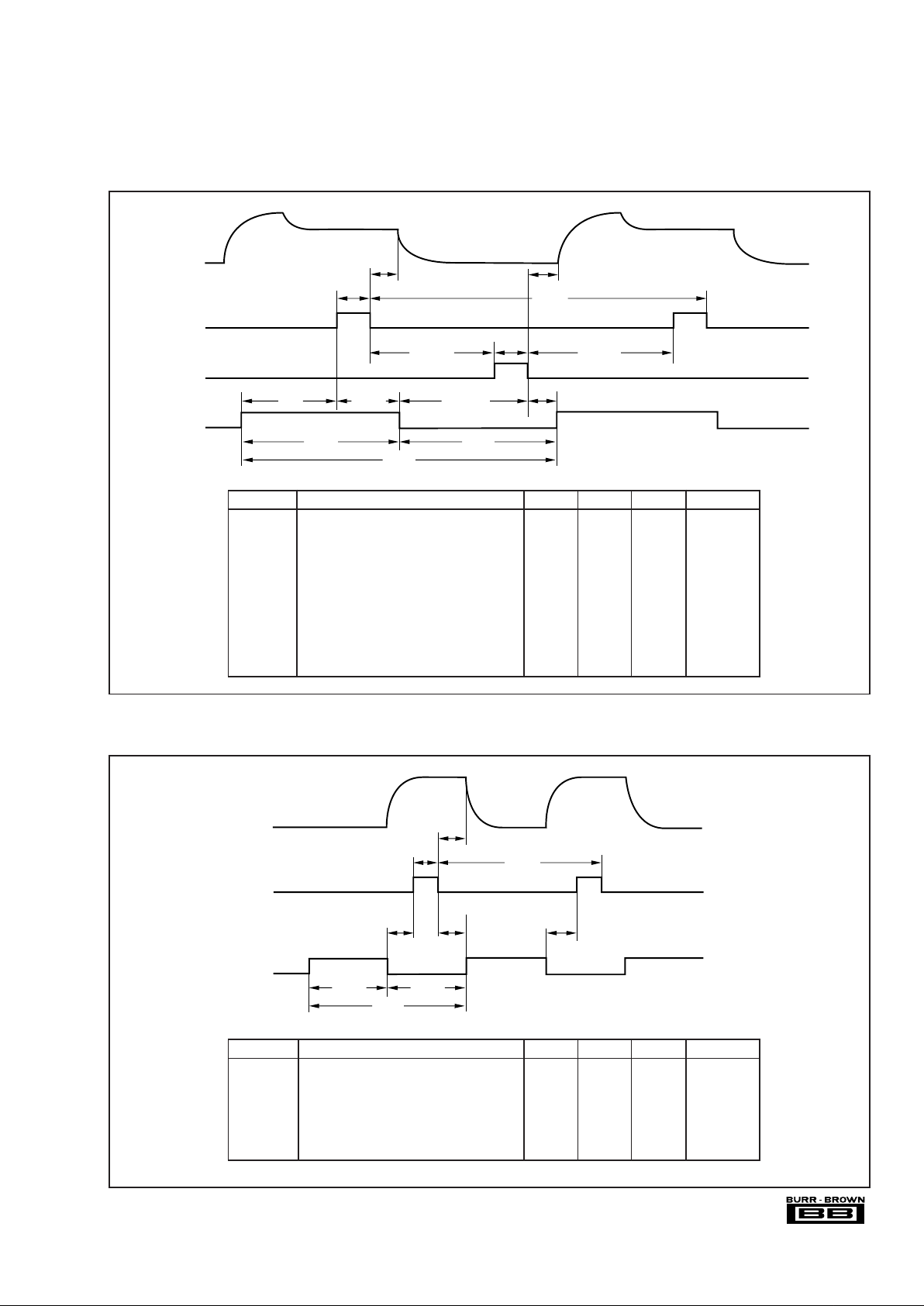
SYMBOL PARAMETER MIN TYP MAX UNITS
t
CK1W-1
CK1 Pulse Width 20 40 ns
t
CK1P-1
1-Channel Mode Conversion Rate 100 166 ns
t
ADCW
ADCCK Pulse Width 41 83 ns
t
ADCP
ADCCK Period 83 166 ns
t
S
Sampling Delay 10 ns
t
SET
ADCCK Falling to CK1 Rising 10 ns
t
CNV
Conversion Delay 40 ns
1-Channel CIS Mode Timing
CIS Output
CK1
ADCCK
t
S
t
CK1P-1
t
SET
t
CNV
t
ADCW
t
ADCW
t
ADCP
t
CK1W-1
t
SET
Pixel 1
Pixel 1 Pixel 2
Pixel 2
6
®
VSP3100
TIMING DIAGRAMS (Cont.)
Timing Specifications: VCC = +5V supply and normal output mode with the specified temperature range, unless otherwise noted.
SYMBOL PARAMETER MIN TYP MAX UNITS
t
CK1W-3
CK1 Pulse Width 20 125 ns
t
CK1P-3
3-Channel Mode Conversion Rate 300 500 ns
t
CK2W-3
CK2 Pulse Width 20 125 ns
t
CK1CK2-3
CK1 Falling to CK2 Rising 15 ns
t
CK2CK1-3
CK2 Falling to CK1 Rising 70 ns
t
ADCCK2-3
ADCCK Falling to CK2 Falling 5 ns
t
ADCW
ADCCK Pulse Width 41 83 ns
t
ADCP
ADCCK Period 83 166 ns
t
S
Sampling Delay 10 ns
t
SET
ADCCK Rising to CK1 Rising 10 ns
t
CNV
Conversion Delay 40 ns
3-Channel CCD Mode Timing
t
ADCP
t
ADCW
t
SET
t
SET
t
CK1CK2-3
t
CK2CK1-3
t
CNV
t
S
t
S
t
CK2W-3
t
ADCW
t
ADCCK2-3
t
CK1W-3
t
CK1P-3
(R)
(G)
(B) Pixel 1 (R)
Pixel 1 (R/G/B) Pixel 2 (R/G/B)
Pixel 1 (G) Pixel 1 (B)
CCD Output
CK1
CK2
ADCCK
 Loading...