

Burr Brown VSP3010Y-2K, VSP3010Y Datasheet
®
VSP3010
12-Bit, 12MHz
CCD/CIS SIGNAL PROCESSOR
FEATURES
●
12-BIT, 12MHz A/D CONVERTER
● GUARANTEED NO MISSING CODES
● 3-CHANNEL, 4MHz COLOR SCAN MODE:
Correlated Double Samplers
8-Bit Offset Adjustment DACs
0dB to +13dB PGAs
● A/D INPUT MONITOR
● INTERNAL VOLTAGE REFERENCE
● SINGLE +5V SUPPLY
● 3V OR 5V DIGITAL OUTPUT
● LOW POWER: 500mW typ (CCD Mode)
DESCRIPTION
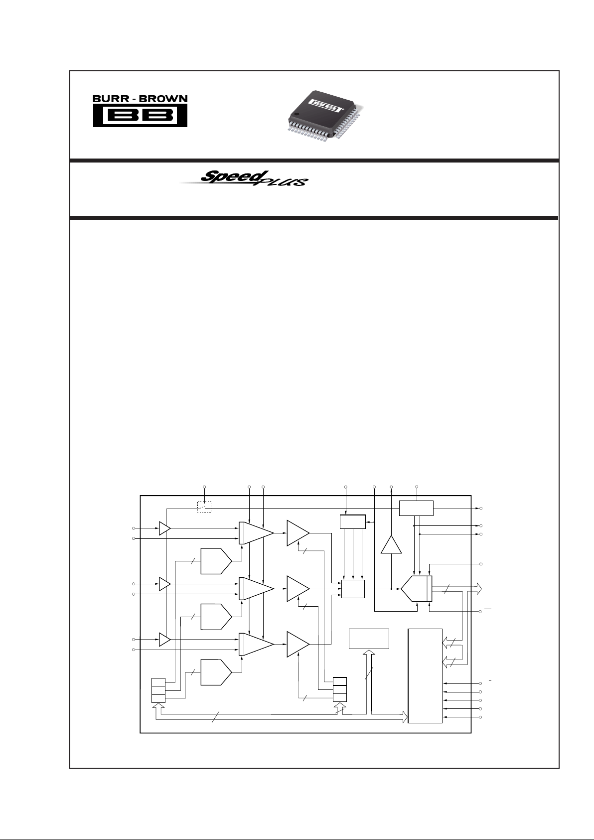
The VSP3010 is a complete, three-channel image
signal processor for Charge Coupled Device (CCD)
or Contact Image Sensor (CIS) systems. Each channel contains sensor signal sampling, Black Level
adjustment and a programmable gain amplifier. The
three inputs are multiplexed into a high speed, 12-bit
analog-to-digital converter. Input circuitry can be
configured, by digital command, for CCD or CIS
sensors. A Black Clamp and Correlated Double
Samplers (CDS) are provided for CCD sensors. For
CIS devices, the VSP3010 provides a single-ended
sampler and a reference input. The VSP3010 is
available in a 48-lead LQFP package and operates
from 0°C to +85°C with a single +5V supply.
TM
©
1999 Burr-Brown Corporation PDS-1542A Printed in U.S.A. June, 1999
APPLICATIONS
● CCD AND CIS COLOR SCANNERS
● FAX AND MULTI-FUNCTION MACHINES
● INDUSTRIAL / MEDICAL IMAGING SYSTEMS
VSP3010
International Airport Industrial Park • Mailing Address: PO Box 11400, Tucson, AZ 85734 • Street Address: 6730 S. Tucson Blvd., Tucson, AZ 85706 • Tel: (520) 746-1111
Twx: 910-952-1111 • Internet: http://www.burr-brown.com/ • Cable: BBRCORP • Telex: 066-6491 • FAX: (520) 889-1510 • Immediate Product Info: (800) 548-6132
For most current data sheet and other product
information, visit www.burr-brown.com
8
5
RINP
RINN
Clamp
8
5
GINP
GINN
Clamp
8
5
5
8
8
3
8
12
CDS
CDS
CDS
PGA
PGA
PGA
BINP
BINN
Clamp
8-Bit
DAC
8-Bit
DAC
8-Bit
DAC
MUX
Timing
Bandgap
Reference
R
G
B
Offset
Register
R
G
B
Gain
Adjust
Register
Configuration
Register
Register
Port
M1
M2
M3
12-Bit
A/D
P/S
WRT
RD
SCLK
SD
CM
REFT
REFB
OE
V
DRV
B0-B11
(D0-D7, A0-A2)
VSP3010
CK1CLP CK2 STRT
V
REF
ADCCK TP0
®
2
VSP3010
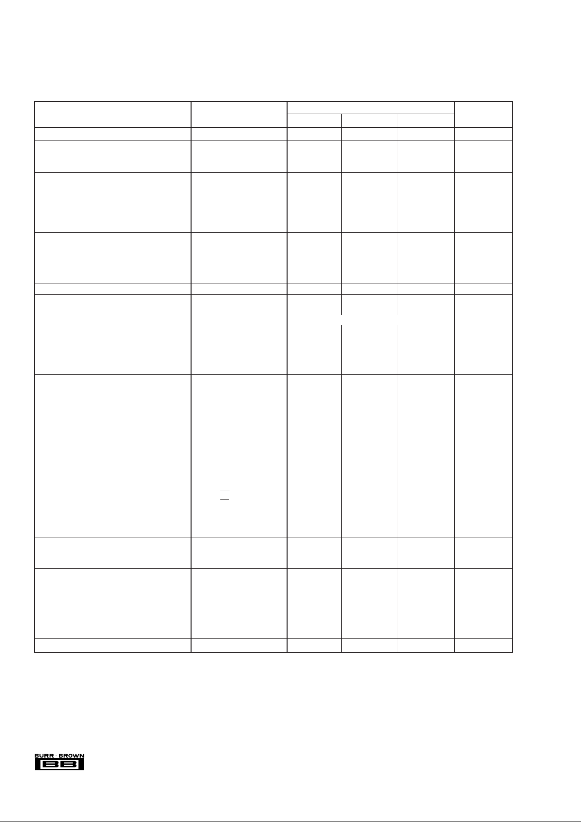
SPECIFICATIONS
At TA = full specified temperature range, V
DDA
= +5V, V
DDD
= +5V, f
ADCCK
= 6MHz, f
CK1
= 2MHz, f
CK2
= 2MHz, and PGA gain = 1, unless otherwise specified.
VSP3010Y
PARAMETER CONDITIONS MIN TYP MAX UNITS
RESOLUTION 12 Bits
CONVERSION CHARACTERISTICS
3-Channel CCD Mode 12 MHz
3-Channel CIS Mode 12 MHz
ANALOG INPUTS
Full-Scale Input Range 0.5 3.5 Vp-p
Input Capacitance 10 pF
External Reference Voltage Range 0.25 1.75 V
Reference Input Resistance 800 Ω
Input Limits GND
A
– 0.3 V
DDA
+ 0.3 V
DYNAMIC CHARACTERISTICS
Integral Non-Linearity (INL) ±1 ±2 LSB
Differential Non-Linearity (DNL) 0.3 0.75 LSB
No Missing Codes 12 Bits
Input-Referred Noise 0.3 LSBs rms
PSRR V
DDA
= +5V ±0.25V 0.04 % FSR
DIGITAL INPUTS
Logic Family CMOS
Convert Command Start Conversion Rising Edge of ADCCK
High Level Input Current (V
IN
= V
DDD
) 20 µA
Low Level Input Current (VIN = 0V) 20 µA
Positive-Going Threshold Voltage 3.00 3.40 3.80 V
Negative-Going Threshold Voltage 1.25 1.65 2.05 V
Input Capacitance 5pF
DIGITAL OUTPUTS
Logic Family CMOS
Logic Coding Straight Binary
V
DRV
Supply Range +2.7 +5.3 V
Output Voltage, V
DRV
= +5V
Low Level I
OL
= 50µA +0.1 V
High Level IOH = 50µA +4.6 V
Low Level IOL = 1.6mA +0.4 V
High Level I
OH
= 0.5mA +2.4 V
Output Voltage, V
DRV
= +3
Low Level IOL = 50µA +0.1 V
High Level I
OH
= 50µA +2.5 V
3-State Enable Time OE = LOW 20 40 ns
3-State Enable Time OE = HIGH 2 10 ns
Output Capacitance 5pF
Data Latency 6 Clock Cycles
Data Output Delay C
L
= 15pF 12 ns
DC ACCURACY
Zero Error 0.8 % FS
Gain Error 1.5 % FS
POWER SUPPLY REQUIREMENTS
Supply Voltage: +V
S
Operating 4.7 5 5.3 V
Supply Current: +I
S
3-Channel Mode 100 108 mA
1-Channel Mode 82 90 mA
Power Dissipation 3-Channel Mode 500 540 mW
1-Channel Mode 410 450 mW
Thermal Resistance,
θ
JA
100 °C/W
SPECIFIED TEMPERATURE RANGE 0 +85 °C
®
3
VSP3010
The information provided herein is believed to be reliable; however, BURR-BROWN assumes no responsibility for inaccuracies or omissions. BURR-BROWN
assumes no responsibility for the use of this information, and all use of such information shall be entirely at the user’s own risk. Prices and specifications are subject
to change without notice. No patent rights or licenses to any of the circuits described herein are implied or granted to any third party. BURR-BROWN does not
authorize or warrant any BURR-BROWN product for use in life support devices and/or systems.
Supply Voltage, (V
DDA, VDDD,VDRV
) ......................................................+6V
Analog Input .......................................................(–0.3V) to (+V
DDA
+ 0.3V)
Logic Input ......................................................... (–0.3V) to (+V
DDD
+ 0.3V)
Operating Temperature ........................................................ 0°C to +85°C
Case Temperature ......................................................................... +100°C
Junction Temperature .................................................................... +150°C
Storage Temperature..................................................................... +150°C
ABSOLUTE MAXIMUM RATINGS
ELECTROSTATIC
DISCHARGE SENSITIVITY
This integrated circuit can be damaged by ESD. Burr-Brown
recommends that all integrated circuits be handled with
appropriate precautions. Failure to observe proper handling
and installation procedures can cause damage.
ESD damage can range from subtle performance degradation
to complete device failure. Precision integrated circuits may
be more susceptible to damage because very small parametric
changes could cause the device not to meet its published
specifications.
PACKAGE SPECIFIED
DRAWING TEMPERATURE PACKAGE ORDERING TRANSPORT
PRODUCT PACKAGE NUMBER
(1)
RANGE MARKING NUMBER
(2)
MEDIA
VSP3010Y LQFP-48 340 0°C to +85°C VSP3010Y VSP3010Y 250-Piece Tray
"""""VSP3010Y/2K Tape and Reel
NOTES: (1) For detailed drawing and dimension table, please see end of data sheet, or Appendix C of Burr-Brown IC Data Book. (2) Models with a slash (/ ) are
available only in Tape and Reel in the quantities indicated (e.g., /2K indicates 2000 devices per reel). Ordering 2000 pieces of “VSP3010Y/2K” will get a single 2000piece Tape and Reel. For detailed Tape and Reel mechanical information, refer to Appendix B of Burr-Brown IC Data Book.
PACKAGE/ORDERING INFORMATION
®
4
VSP3010
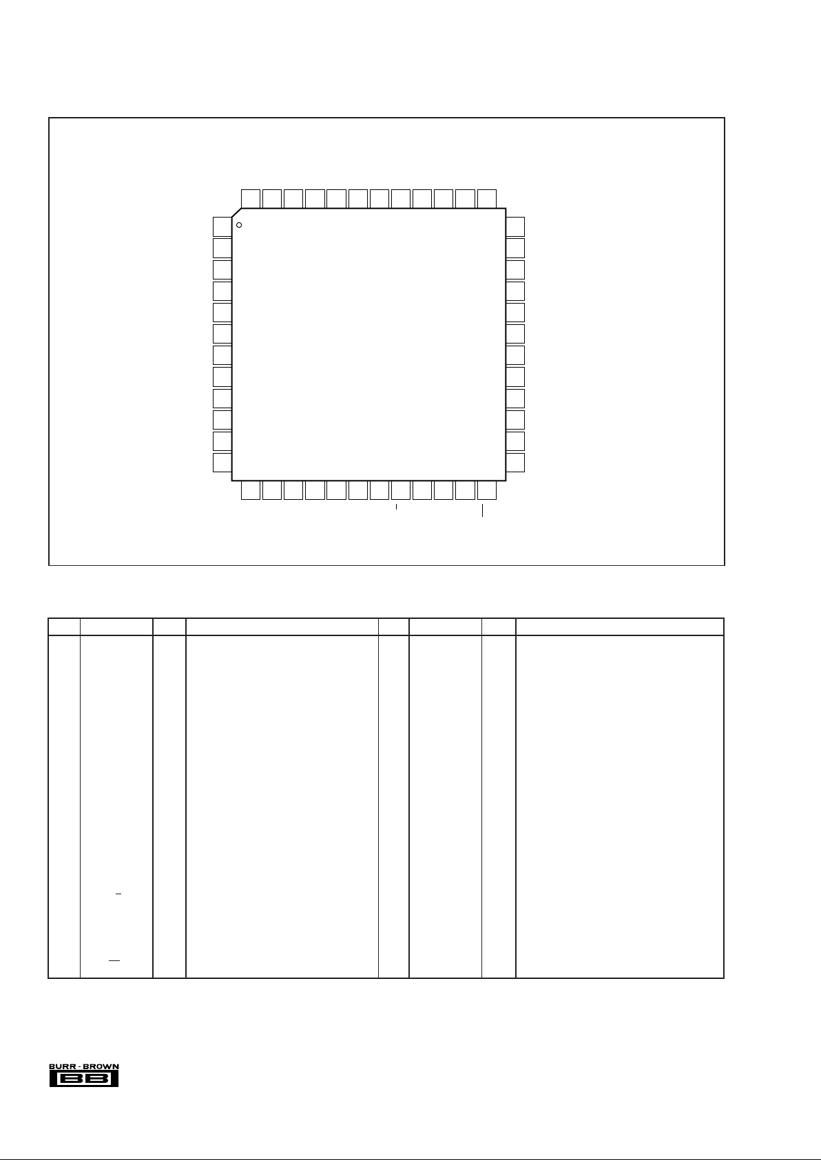
PIN DESCRIPTIONS
PIN DESIGNATOR TYPE DESCRIPTION PIN DESIGNATOR TYPE DESCRIPTION
1 CLP DI Clamp Enable
2 GND
A
P Analog Ground
3 RINP AI Red-Channel Analog Input
4 RINN AI Red-Channel Reference Input
5 GND
A
P Analog Ground
6 GINP AI Green-Channel Analog Input
7 GINN AI Green-Channel Reference Input
8 GND
A
P Analog Ground
9 BINP AI Blue-Channel Analog Input
10 BINN AI Blue-Channel Reference Input
11 GND
A
P Analog Ground
12 V
DDA
P Analog Power Supply, +5V
13 STRT DI Start Line Scanning
14 ADCCK DI A/D Converter Clock Input
15 CK1 DI Sample Reference Clock
16 CK2 DI Sample Data Clock
17 GND
D
P Digital Ground
18 RD DI Read Signal for Registers
19 WRT DI Write Signal for Registers
20 P/S DI Parallel/Serial Port Select;
HIGH = Parallel, LOW = Serial
21 SD DI Serial Data Input
22 SCLK DI Serial Data Clock
23 V
DDD
P Digital Power Supply, +5V
24 OE DI A/D Converter Output Enable
25 B0 (D0) LSB DIO
A/D Output (Bit 0) and Register Data Port (Bit 0)
26 B1 (D1) DIO
A/D Output (Bit 1) and Register Data Port (Bit 1)
27 B2 (D2) DIO
A/D Output (Bit 2) and Register Data Port (Bit 2)
28 B3 (D3) DIO
A/D Output (Bit 3) and Register Data Port (Bit 3)
29 B4 (D4) DIO
A/D Output (Bit 4) and Register Data Port (Bit 4)
30 B5 (D5) DIO
A/D Output (Bit 5) and Register Data Port (Bit 5)
31 B6 (D6) DIO
A/D Output (Bit 6) and Register Data Port (Bit 6)
32 B7 (D7) DIO
A/D Output (Bit 7) and Register Data Port (Bit 7)
33 B8 (A0) DIO A/D Output (Bit 8) and Register Address (Bit 0)
34 B9 (A1) DIO A/D Output (Bit 9) and Register Address (Bit 1)
35 B10 (A2) DIO A/D Output (Bit 10) and Register Address (Bit 2)
36 B11 MSB DO A/D Output (Bit 11)
37 V
DRV
P Output Driver Voltage Supply
38 V
DDD
P Digital Power Supply, +5V
39 GND
D
P Digital Ground
40 TP0 AO A/D Converter Input Monitor Pin
41 GND
A
P Analog Ground
42 V
DDA
P Analog Power Supply, +5V
43 V
REF
AIO Reference Input/Output
44 GND
A
P Analog Ground
45 REFB AO Bottom Reference
46 CM AO Common-Mode Voltage
47 REFT AO Top Reference
48 V
DDA
P Analog Power Supply, +5V
PIN CONFIGURATION
36
35
34
33
32
31
30
29
28
27
26
25
B11 (MSB)
B10 (A2)
B9 (A1)
B8 (A0)
B7 (D7)
B6 (D6)
B5 (D5)
B4 (D4)
B3 (D3)
B2 (D2)
B1 (D1)
B0 (D0, LSB)
V
DDA
REFTCMREFB
GNDAV
REFVDDA
GNDATP0
GNDDV
DDDVDRV
STRT
ADCCK
CK1
CK2
GND
D
RD
WRT
P/S
SD
SCLK
V
DDD
OE
1
2
3
4
5
6
7
8
9
10
11
12
CLP
GND
A
RINP
RINN
GND
A
GINP
GINN
GND
A
BINP
BINN
GND
A
V
DDA
48 47 46 45 44 43 42 41 40 39 38
13 14 15 16 17 18 19 20 21 22 233724
VSP3010Y
®
5
VSP3010
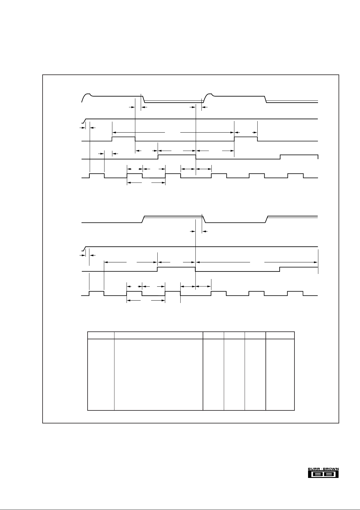
TIMING DIAGRAMS
Timing specifications = t
MIN
to t
MAX
with +5V power supply.
SYMBOL PARAMETER MIN TYP MAX UNITS
t
CK1AP
3-Channel Conversion Rate 200 250 ns
t
CK1A
CK1 Pulse Width 15 70 ns
t
CK2A
CK2 Pulse Width 15 70 ns
t
CCK
ADCCK Pulse Width 35 42 ns
t
CKP
ADCCK Period 83 ns
t
S
Sampling Delay 10 ns
t
CK12A
CK1 Falling Edge to CK2 Rising Edge 15 ns
t
CK21A
CK2 Falling Edge to CK1 Rising Edge 50 ns
t
SET
ADCCK Falling Edge to CK1 Rising Edge 10 ns
t
ADCCK2
ADCCK Falling Edge to CK2 Falling Edge 20 ns
t
ADCCK1
ADCCK Falling Edge to CK1 Falling Edge 20 ns
t
CNV
Conversion Delay 22 ns
t
ST
Start Conversion Time 20 100 ns
Timing for 3-Channel CCD/CIS Mode
t
CKP
t
CCK
t
CCK
t
CNV
t
CK12A
t
CK2A
t
CK21A
t
ST
t
SET
t
CK1AP
t
CK1A
t
S
t
S
t
ADCCK2
GRR1G1B1B
R1, G1, B1
CCD
STRT
CK1
CK2
ADCCK
t
CCK
t
ADCCK1tCNV
t
CCK
t
SET
t
CKP
t
S
GRR1G1B1B
t
CK1A
R1, G1, B1
t
CK1AP
t
ST
CIS
STRT
CK1
ADCCK
3-Channel CCD Mode
3-Channel CIS Mode
 Loading...