

1
®
VSP2212
®
VSP2212
CCD SIGNAL PROCESSOR
For Digital Cameras
FEATURES
● CCD SIGNAL PROCESSING:
Correlated Double Sampling (CDS)
Programmable Black Level Clamping
● PROGRAMMABLE GAIN AMPLIFIER (PGA):
–6 to +42dB Gain Ranging
● 12-BIT DIGITAL DATA OUTPUT:
Up to 20MHz Conversion Rate
No Missing Codes
● 79dB SIGNAL-TO-NOISE RATIO
● ON-CHIP GENERAL-PURPOSE 8-BIT
DIGITAL-TO-ANALOG CONVERTERS
● PORTABLE OPERATION:
Low Voltage: 2.7V to 3.6V
Low Power: 99mW (typ) at 3.0V
Stand-By Mode: 6mW
DESCRIPTION
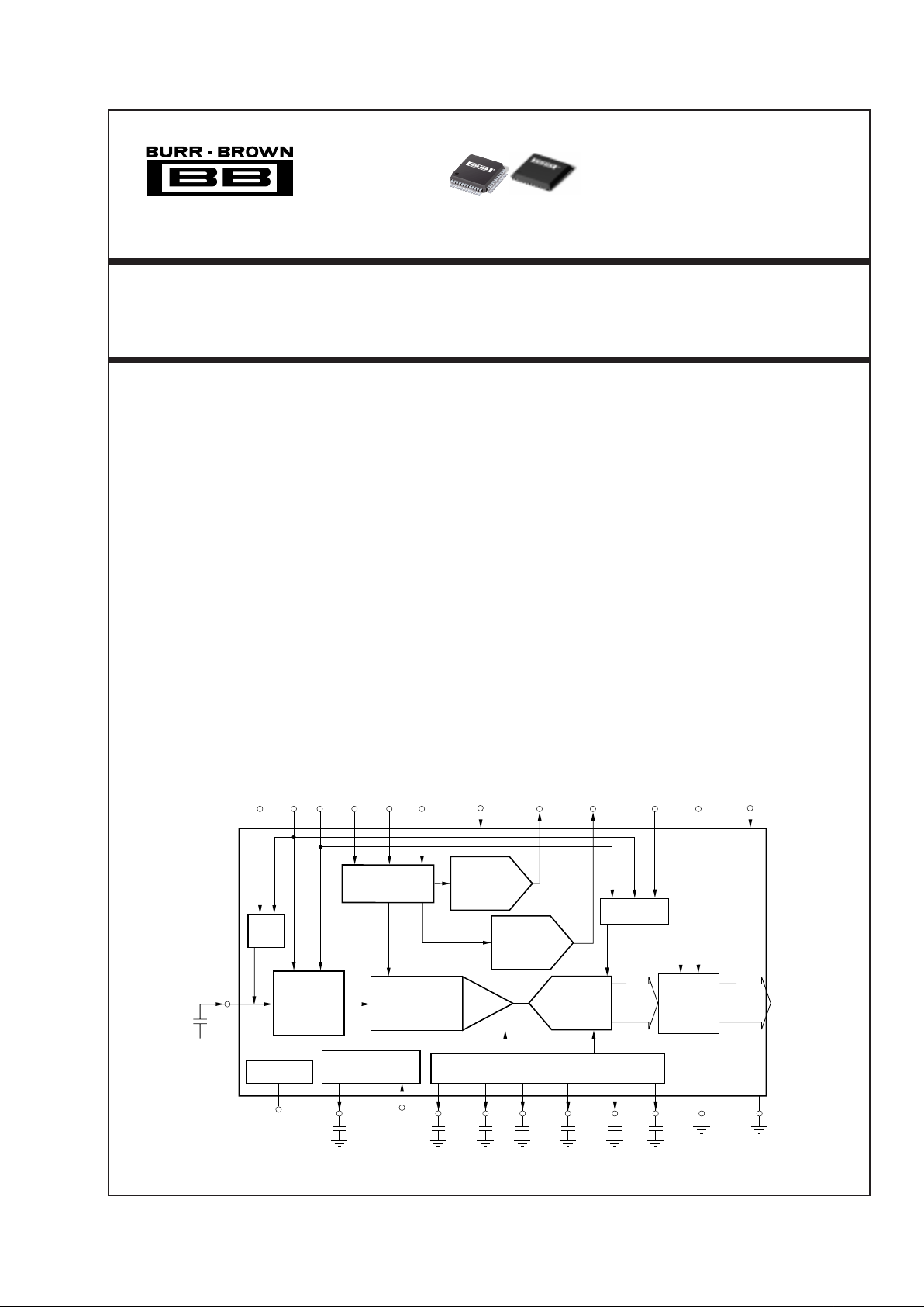
The VSP2212 is a complete mixed-signal processing
IC for digital cameras, providing signal conditioning
and analog-to-digital conversion for the output of a
CCD array. The primary CCD channel provides Correlated Double Sampling (CDS) to extract video information from the pixels, –6dB to +42dB gain ranging
with digital control for varying illumination conditions, and black level clamping for an accurate black
reference. Input signal clamping and offset correction
of the input CDS is also performed. The stable gain
control is linear in dB. Additionally, the black level is
quickly recovered after gain change. The two on-chip
general-purpose 8-bit digital-to-analog converters allow you to obtain analog various control voltage, such
as V
SUB
control of CCD imager. The VSP2212 is the
high-performance version of the VSP2000/2100 families. The VSP2212Y is available in an LQFP-48 package and the VSP2212M is avail able in a VQFN-48
package. Both products operate from a single +3V/
+3.3V supply.
©
2000 Burr-Brown Corporation PDS-1598A Printed in U.S.A. May, 2000
International Airport Industrial Park • Mailing Address: PO Box 11400, Tucson, AZ 85734 • Street Address: 6730 S. Tucson Blvd., Tucson, AZ 85706 • Tel: (520) 746-1111
Twx: 910-952-1111 • Internet: http://www.burr-brown.com/ • Cable: BBRCORP • Telex: 066-6491 • FAX: (520) 889-1510 • Immediate Product Info: (800) 548-6132
For most current data sheet and other product
information, visit www.burr-brown.com
8-Bit
D/A Converter
(DAC0)
8-Bit
D/A Converter
(DAC1)
Programmable
Gain
Amplifier
(PGA)
Input
Clamp
Reference Voltage Generator
Preblanking
Timing
Control
Serial Interface
Output
Latch
Correlated
Double
Sampling
(CDS)
Analog
to
Digital
Converter
12-Bit
Digital
Output
–6dB
to
+42dB
CCDIN
CCD
Output
Signal
PBLK
Optical Black (OB)
Level Clamping
COB
CLPOB
SHPCLPDM SHD SLOAD SCLK SDATA
V
CC
RESET
DACOUT0 DACOUT1 DRV
DD
ADCCK
BYPP2 BYP BYPM REFN CM REFP DRVGND GNDA
B[11:0]
VSP2212
VSP2212

2
®
VSP2212
SPECIFICATIONS
At TA = full specified temperature range, VCC = +3.0V, DRVDD = +3.0V, conversion rate (f
ADDCK
) = 20MHz, unless otherwise specified.
VSP2212Y
PARAMETER CONDITIONS MIN TYP MAX UNITS
RESOLUTION 12 Bits
MAXIMUM CONVERSION RATE 20 MHz
DIGITAL INPUT
Logic Family TTL
Input Voltage LOW to HIGH Threshold Voltage (VT+) 1.7 V
HIGH to LOW Threshold Voltage (VT–) 1.0 V
Input Current Logic HIGH (I
IH
), VIN = +3V ±20 µA
Logic LOW (I
IL
), VIN = 0V ±20 µA
ADCCK Clock Duty Cycle 50 %
Input Capacitance 5pF
Maximum Input Voltage –0.3 5.3 V
DIGITAL OUTPUT
Logic Family CMOS
Logic Coding Straight Binary
Output Voltage Logic HIGH (V
OH
), IOH = –2mA 2.4 V
Logic LOW (V
OL
), IOL = 2mA 0.4 V
ANALOG INPUT (CCDIN)
Input Signal Level for Full-Scale Out PGA Gain = 0dB 900 mV
Input Capacitance 15 pF
Input Limit –0.3 3.3 V
TRANSFER CHARACTERISTICS
Differential Non-Linearity (DNL) PGA Gain = 0dB ±0.5 LSB
Integral Non-Linearity (INL) PGA Gain = 0dB ±1 LSB
No Missing Codes Guaranteed
Step Response Settling Time Full-Scale Step Input 1 Pixels
Overload Recovery Time Step Input from 1.8V to 0V 2 Pixels
Data Latency 9 (fixed) Clock Cycles
Signal-to-Noise Ratio
(1)
Grounded Input Cap, PGA Gain = 0dB
79 dB
Grounded Input Cap, Gain = +24dB
55 dB
CCD Offset Correction Range –180 200 mV
CDS
Reference Sample Settling Time Within 1 LSB, Driver Impedance = 50Ω 11 ns
Data Sample Settling Time Within 1 LSB, Driver Impedance = 50Ω 11 ns
INPUT CLAMP
Clamp-On Resistance 400 Ω
Clamp Level 1.5 V
PROGRAMMABLE GAIN AMPLIFIER (PGA)
Gain Control Resolution 10 Bits
Maximum Gain Gain Code = 1111111111 42 dB
High Gain Gain Code = 1101001000 34 dB
Medium Gain Gain Code = 1000100000 20 dB
Low Gain Gain Code = 0010000000 0 dB
Minimum Gain Gain Code = 0000000000 –6 dB
Gain Control Error ±0.5 dB
OPTICAL BLACK CLAMP LOOP
Control DAC Resolution 10 Bits
Optical Black Clamp Level Programmable Range of Clamp Level 2 242 LSB
OBCLP Level at CODE = 1000 130 LSB
Minimum Output Current for Control DAC COB Pin ±0.15 µA
Maximum Output Current for Control DAC COB Pin ±153 µA
Loop Time Constant C
COB
= 0.1µF 40.7 µs
Slew Rate C
COB
= 0.1µF, Output Current 1530 V/s
from Control DAC is Saturated
GENERAL-PURPOSE 8-BIT DAC (DAC0, DAC1)
Minimum Output Voltage Input Code = 00000000 0.1 V
Maximum Output Voltage Input Code = 11111111 2.9 V
Differential Non-Linearity (DNL) At Input Code = 16 to 224 ±0.25 LSB
Integral Non-Linearity (INL) At Input Code = 16 to 192 ±1 LSB
Offset Error ±200 mV
Gain Error ±5%
Monotonicity Guaranteed
NOTE: (1) SNR = 20 log (full-scale voltage/rms noise).
3
®
VSP2212
Supply Voltage
(2)
.............................................................................................................. +4.0V
Supply Voltage Differences
(3)
.................................................................................. ±0.1V
Ground Voltage Differences
(4)
................................................................................. ±0.1V
Digital Input Voltage ............................................................ –0.3V to 5.3V
Analog Input Voltage ................................................ –0.3V to V
CC
+ 0.3V
Input Current (any pins except supplies) ....................................... ±10mA
Operating Temperature .................................................. –25°C to +85°C
Storage Temperature ..................................................... –55°C to +125°C
Junction Temperature .................................................................... +150°C
Lead Temperature (soldering, 5s) ................................................. +260°C
Package Temperature (IR reflow, peak, 10s) ............................... +235°C
NOTES: (1) Stresses above those listed under Absolute Maximum Ratings
may cause permanent damage to the device. Exposure to absolute maximum
conditions for extended periods may affect device reliability.
(2) V
CC
, DRVDD. (3) Among VCC. (4) Among GNDA and DRVGND.
ABSOLUTE MAXIMUM RATINGS
(1)
ELECTROSTATIC
DISCHARGE SENSITIVITY
This integrated circuit can be damaged by ESD. Burr-Brown
recommends that all integrated circuits be handled with
appropriate precautions. Failure to observe proper handling
and installation procedures can cause damage.
ESD damage can range from subtle performance degradation to complete device failure. Precision integrated circuits
may be more susceptible to damage because very small
parametric changes could cause the device not to meet its
published specifications.
PACKAGE SPECIFIED
DRAWING TEMPERATURE PACKAGE ORDERING TRANSPORT
PRODUCT PACKAGE NUMBER RANGE MARKING NUMBER
(1)
MEDIA
VSP2212Y LQFP-48 340 –25°C to +85°C VSP2212Y VSP2212Y 250-Piece Tray
"""""VSP2212Y/2K Tape and Reel
VSP2212M VQFN-48 369 –25°C to +85°C VSP2212M VSP2212M 250-Piece Tray
"""""VSP2212Y/2M Tape and Reel
NOTE: (1) Models with a slash (/) are available only in Tape and Reel in the quantities indicated (e.g., /2K indicates 2000 devices per reel). Ordering 2000 pieces
of “VSP2212Y/2K” will get a single 2000-piece Tape and Reel.
PACKAGE/ORDERING INFORMATION
The information provided herein is believed to be reliable; however, BURR-BROWN assumes no responsibility for inaccuracies or omissions. BURR-BROWN
assumes no responsibility for the use of this information, and all use of such information shall be entirely at the user’s own risk. Prices and specifications are subject
to change without notice. No patent rights or licenses to any of the circuits described herein are implied or granted to any third party. BURR-BROWN does not
authorize or warrant any BURR-BROWN product for use in life support devices and/or systems.
REFERENCE
Positive Reference Voltage 1.75 V
Negative Reference Voltage 1.25 V
POWER SUPPLY
Supply Voltage V
CC
, DRV
DD
2.7 3.0 3.6 V
Power Dissipation
Normal Operation Mode
No Load, DAC0 and DAC1 are Suspended
99 mW
Stand-By Mode f
ADDCK
= NOT Apply 6 mW
TEMPERATURE RANGE
Operating Temperature –25 +85 °C
Storage Temperature –55 +125 °C
Thermal Resistance,
θ
JA
LQFP-48 100 °C/W
VSP2212Y
PARAMETER CONDITIONS MIN TYP MAX UNITS
SPECIFICATIONS (Cont.)
At TA = full specified temperature range, VCC = +3.0V, DRVDD = +3.0V, conversion rate (f
ADDCK
) = 20MHz, unless otherwise specified.
PRODUCT ORDERING NUMBER
VSP2212Y DEM-VSP2212Y
DEMO BOARD ORDERING INFORMATION
4
®
VSP2212
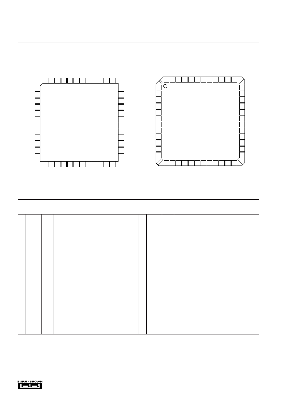
PIN CONFIGURATION
36
35
34
33
32
31
30
29
28
27
26
25
GNDA
GNDA
V
CC
V
CC
BYPM
BYP
CCDIN
BYPP2
COB
V
CC
GNDA
GNDA
SCLK
SDATA
SLOAD
RESET
DACOUT1
DACOUT0
GNDA
GNDA
VCCREFN
REFP
CM
DRV
DD
DRVGND
GNDA
ADCCK
GNDA
V
CC
PBLK
CLPOB
SHP
SHD
CLPDM
V
CC
1
2
3
4
5
6
7
8
9
10
11
12
B0 (LSB)
B1
B2
B3
B4
B5
B6
B7
B8
B9
B10
B11 (MSB)
48 47 46 45 44 43 42
41 40 39 38
13 14 15 16 17 18 19 20 21 22 233724
VSP2212
25 GNDA P Analog Ground
26 GNDA P Analog Ground
27 V
CC
P Analog Power Supply
28 COB AO Optical Black Clamp Loop Reference (Bypass to Ground
(3)
)
29 BYPP2 AO Internal Reference P (Bypass to Ground
(4)
)
30 CCDIN AI CCD Signal Input
31 BYP AO Internal Reference C (Bypass to Ground
(5)
)
32 BYPM AO Internal Reference N (Bypass to Ground
(4)
)
33 V
CC
P Analog Power Supply
34 V
CC
P Analog Power Supply
35 GNDA P Analog Ground
36 GNDA P Analog Ground
37 CM AO
A/D Converter Common-Mode Voltage (Bypass to Ground
(5)
)
38 REFP AO A/D Converter Positive Reference (Bypass to Ground
(5)
)
39 REFN AO A/D Converter Negative Reference (Bypass to Ground
(5)
)
40 V
CC
P Analog Power Supply
41 GNDA P Analog Ground
42 GNDA P Analog Ground
43
DACOUT0
AO General-Purpose 8-Bit D/A Converter
(DAC0) Output Voltage
44
DACOUT1
AO General-Purpose 8-Bit D/A Converter
(DAC1) Output Voltage
45 RESET DI Asynchronous System Reset (Active LOW)
46 SLOAD DI Serial Data Latch Signal (Triggered at the Rising Edge)
47 SDATA DI Serial Data Input
48 SCLK DI Clock for Serial Data Shift (Triggered at the Rising Edge)
PIN NAME TYPE
(1)
DESCRIPTION
1 B0 (LSB) DO Bit 0, A/D Converter Output, Least Significant Bit
2 B1 DO Bit 1, A/D Converter Output
3 B2 DO Bit 2, A/D Converter Output
4 B3 DO Bit 3, A/D Converter Output
5 B4 DO Bit 4, A/D Converter Output
6 B5 DO Bit 5, A/D Converter Output
7 B6 DO Bit 6, A/D Converter Output
8 B7 DO Bit 7, A/D Converter Output
9 B8 DO Bit 8, A/D Converter Output
10 B9 DO Bit 9, A/D Converter Output
11 B10 DO Bit 10, A/D Converter Output
12
B11 (MSB)
DO Bit 11, A/D Converter Output, Most Significant Bit
13 DRV
DD
P Power Supply, Exclusively for Digital Output
14 DRVGND P Digital Ground, Exclusively for Digital Output
15 GNDA P Analog Ground
16 ADCCK DI Clock for Digital Output Buffer
17 GNDA P Analog Ground
18 V
CC
P Analog Power Supply
19 PBLK DI Preblanking:
HIGH = Normal Operation Mode
LOW = Preblanking Mode: Digital Output “All Zero”
20 CLPOB DI Optical Black Clamp Pulse (Default = Active LOW
(2)
)
21 SHP DI
CDS Reference Level Sampling Pulse (Default = Active LOW
(2)
)
22 SHD DI CDS Data Level Sampling Pulse (Default = Active LOW
(2)
)
23 CLPDM DI Dummy Pixel Clamp Pulse (Default = Active LOW
(2)
)
24 V
CC
P Analog Power Supply
PIN NAME
TYPE
(1)
DESCRIPTION
PIN DESCRIPTIONS
NOTES: (1) Type designators: P = Power Supply and Ground; DI = Digital Input; DO = Digital Output; AI = Analog Input; AO = Analog Output. (2) Refer to the “Serial
Interface” section for more detail. (3) Should be connected to ground with a bypass capacitor. We recommend the value of 0.1µF to 0.22 µF, however, it depends
on the application environment. Refer to the “Optical Black Level Clamp Loop” section for more detail. (4) Should be connected to ground with a bypass capacitor.
We recommend the value of 1000pF, however, it depends on the application environment. Refer to the “Voltage Reference” section for more detail. (5) Should be
connected to ground with a bypass capacitor (0.1µF). Refer to the “Voltage Reference” section for more detail.
36
35
34
33
32
31
30
29
28
27
26
25
GNDA
GNDA
V
CC
V
CC
BYPM
BYP
CCDIN
BYPP2
COB
V
CC
GNDA
GNDA
SCLK
SDATA
SLOAD
RESET
DACOUT1
DACOUT0
GNDA
GNDA
VCCREFN
REFP
CM
DRV
DD
DRVGND
GNDA
ADCCK
GNDA
V
CC
PBLK
CLPOB
SHP
SHD
CLPDM
V
CC
1
2
3
4
5
6
7
8
9
10
11
12
B0 (LSB)
B1
B2
B3
B4
B5
B6
B7
B8
B9
B10
B11 (MSB)
48 47 46 45 44 43 42
41 40 39 38
13 14 15 16 17 18 19 20 21 22 233724
VSP2212M
Top View LQFP Top View VQFN
 Loading...