

Burr Brown VSP2101Y-2K, VSP2101Y Datasheet
®
VSP2101
CCD SIGNAL PROCESSOR
For Digital Cameras
FEATURES
● CCD SIGNAL PROCESSING:
Correlated Double Sampling
Black Level Clamping
–2 to +34dB Gain Ranging
High SNR: 53dB
● 10-BIT A/D CONVERSION:
Up to 27MHz Conversion Rate
No Missing Codes
● PORTABLE OPERATION:
Low Voltage: 2.7V to 3.6V
Low Power: 190mW at 3.0V
● LOW POWER: 160mW at 2.7V
● POWER-DOWN MODE: 18mW
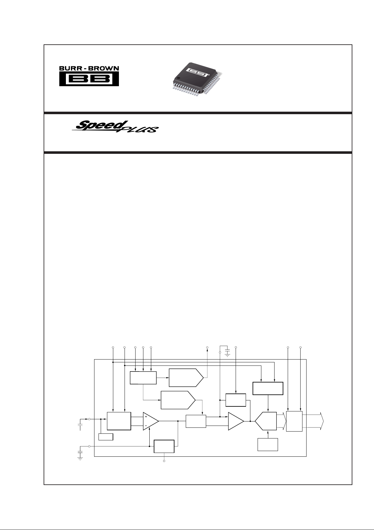
DESCRIPTION
The VSP2101Y is a complete digital camera IC, providing signal conditioning and 10-bit analog-to-digital
conversion for the output of a CCD array.
The primary CCD channel provides correlated double
sampling to extract the video information from the
pixels, –2dB to +34dB gain ranging with digital control for varying illumination conditions, and black
level clamping for an accurate black reference.
Input signal clamping and offset correction of the CDS
is also performed. The stable gain control is linear in
dB. Additionally, the black level is quickly recovered
after gain change. An on-chip general purpose 10-bit
digital-to-analog converter allows you to obtain analog control voltage for iris control.
The VSP2101Y is available in a 48-lead LQFP package and operates from a single +3V supply.
APPLICATIONS
● VIDEO CAMERAS
● DIGITAL STILL CAMERAS
● PC CAMERAS
● SECURITY CAMERAS
©
1998 Burr-Brown Corporation PDS-1506B Printed in U.S.A. June, 1999
TM
International Airport Industrial Park • Mailing Address: PO Box 11400, Tucson, AZ 85734 • Street Address: 6730 S. Tucson Blvd., Tucson, AZ 85706 • Tel: (520) 746-1111
Twx: 910-952-1111 • Internet: http://www.burr-brown.com/ • Cable: BBRCORP • Telex: 066-6491 • FAX: (520) 889-1510 • Immediate Product Info: (800) 548-6132
10-Bit
D/A Converter
(DAC1)
C
10-Bit
D/A Converter
(DAC0)
Log VCA
Clamp
A/D
Reference
Dummy
Pixel
Auto- Zero
Black Level
Auto-Zero
A/D
Timing Control
Serial Port
Register
Output
Latch
Correlated
Double
Sampling
10-Bit
A/D
Converter
10-Bit
Digital
Output
+28dB+6dB
CCD R
CCD D
CCD Out
DUMC
REFCK DATCK WRT SD SCLK DAC OUT
OB
DRV
DD
ADCK
VSP2101

2
®
VSP2101
SPECIFICATIONS
At TA = +25°C, all power supply voltages = +3.0V, and conversion rate = 18MHz, unless otherwise specified.
VSP2101Y
PARAMETER CONDITIONS MIN TYP MAX UNITS
RESOLUTION 10 Bits
DIGITAL INPUT
Logic Family CMOS
Logic Levels Logic HI 2.5 V
Logic LO +0.4 V
Logic Currents Logic HI, V
IN
= +3V 10 µA
Logic LO, VIN = 0V 10 µA
A/D Clock Duty Cycle 50 %
Input Capacitance 5pF
DIGITAL OUTPUT
Logic Family CMOS
Logic Levels Logic HI, C
L
= 10pF 2.5 V
Logic LO, C
L
= 10pF +0.4 V
ANALOG OUTPUT
General Purpose D/A Converter Output
Minimum Output Voltage Control Data = 1023 0.3 V
Maximum Output Voltage Control Data = 0 2.4 V
DAC Settling TIme 1.0 µs
TRANSFER CHARACTERISTICS
Differential Non-Linearity ±0.5 LSB
Integral Non-Linearity 2.0 LSB
No Missing Codes Guaranteed
Signal Settling Time Black to Full-Scale Change 110 ns
to 1/4 LSB into A/D
Conversion Rate 500kHz 27 MHz
Data Latency 5.5 Clocks
Signal-to-Noise Ratio
(1)
Grounded Input Cap, Maximum Gain
53 dB
CCD Offset Correction Range ±150 mV
Black Clamp Level 32 LSB
CDS
Data Settling Time to ±0.1% for FS Change From Leading Edge 11 ns
with R
S
= 40 of DATCK
Input Signal Level for FS Out Minimum Gain 600 mV
Input Capacitance DATCK LOW 20 pF
Input Time Constant 300 ps
INPUT CLAMP
Clamp-On Resistance 3.3 kΩ
Clamp Level 1.2 V
GAIN CONTROL CHARACTERISTICS
Gain, max Control Data = 0 32 34 dB
Gain, min Control Data = 1023 –2 dB
Gain Control Linearity ±1.0 dB
Gain Control Settling Time 10 µs
POWER SUPPLY
Rated Voltage +2.7 +3.0 +3.6 V
Quiescent Current 63 mA
Power Dissipation 190 mW
Power-Down Mode 18 mW
TEMPERATURE RANGE
Specified Range Ambient –25 +85 °C
Thermal Resistance,
θ
JA
48-Lead LQFP 100 °C/W
NOTE: (1) SNR = 20log (full-scale voltage / r ms noise).
The information provided herein is believed to be reliable; however, BURR-BROWN assumes no responsibility for inaccuracies or omissions. BURR-BROWN
assumes no responsibility for the use of this information, and all use of such information shall be entirely at the user’s own risk. Prices and specifications are subject
to change without notice. No patent rights or licenses to any of the circuits described herein are implied or granted to any third party. BURR-BROWN does not
authorize or warrant any BURR-BROWN product for use in life support devices and/or systems.
3
®
VSP2101
Power Supply (+VS) ............................................................................. +6V
Analog Input.............................................................. –0.3V to (+V
S
+0.3V)
Logic Input ............................................................... –0.3V to (+V
S
+0.3V)
Case Temperature ......................................................................... +100°C
Junction Temperature .................................................................... +150°C
Storage Temperature...................................................... –40°C to +150°C
ABSOLUTE MAXIMUM RATINGS
ELECTROSTATIC
DISCHARGE SENSITIVITY
This integrated circuit can be damaged by ESD. Burr-Brown
recommends that all integrated circuits be handled with
appropriate precautions. Failure to observe proper handling
and installation procedures can cause damage.
ESD damage can range from subtle performance degradation
to complete device failure. Precision integrated circuits may
be more susceptible to damage because very small parametric
changes could cause the device not to meet its published
specifications.
PACKAGE SPECIFIED
DRAWING TEMPERATURE PACKAGE ORDERING TRANSPORT
PRODUCT PACKAGE NUMBER
(1)
RANGE MARKING NUMBER
(2)
MEDIA
VSP2101Y 48-Lead LQFP 340 –25°C to +85°C VSP2101Y VSP2101Y 50-Piece Tray
" " " " " VSP2101Y/2K Tape and Reel
NOTES: (1) For detailed drawing and dimension table, please see end of data sheet, or Appendix C of Burr-Brown IC Data Book. (2) Models with a slash (/ ) are
available only in Tape and Reel in the quantities indicated (e.g., /2K indicates 2000 devices per reel). Ordering 2000 pieces of “VSP2101Y/2K” will get a single 1000piece Tape and Reel.
PACKAGE/ORDERING INFORMATION
4
®
VSP2101
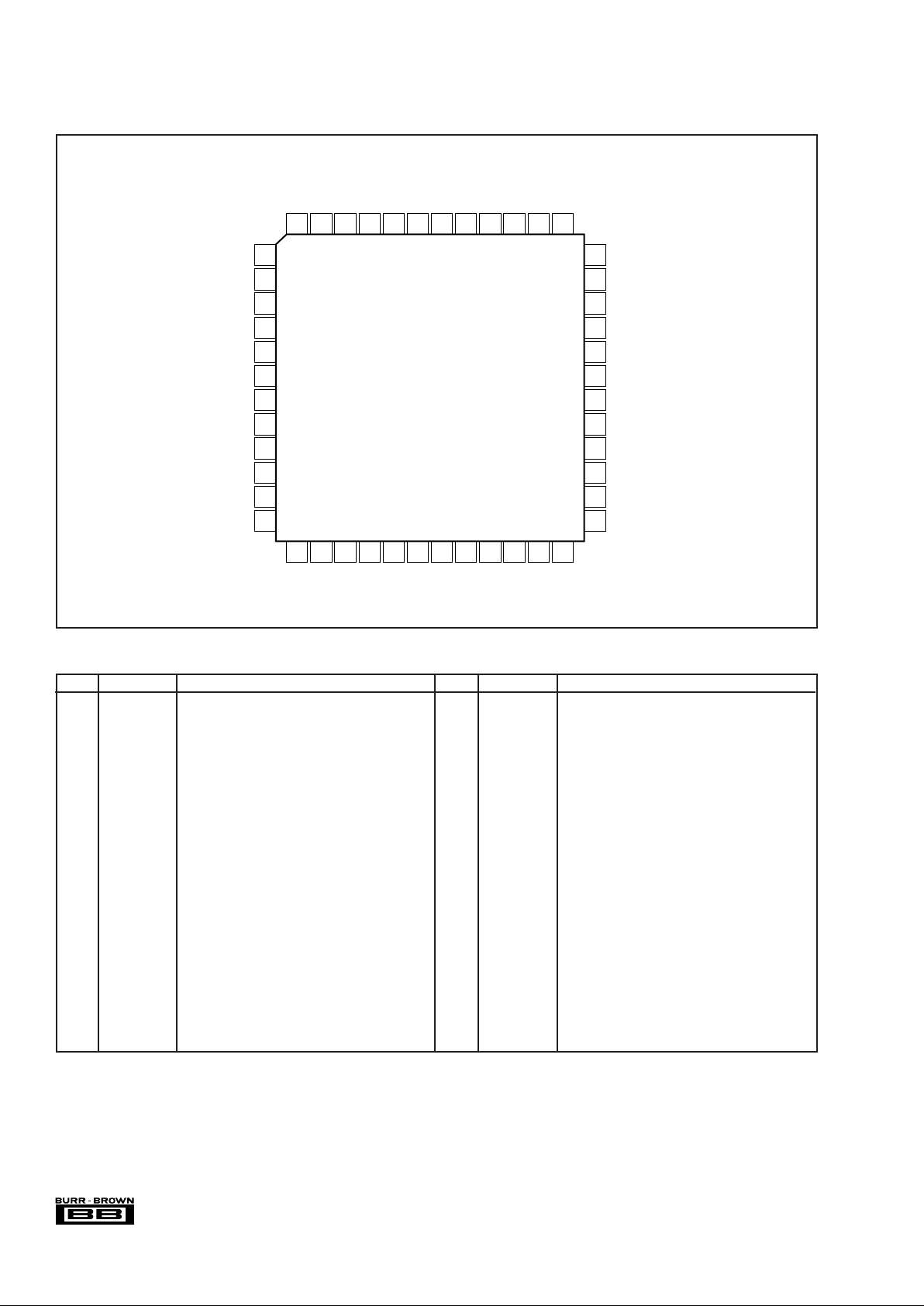
PIN CONFIGURATION
36
35
34
33
32
31
30
29
28
27
26
25
WRT
SCLK
SD
AV
DD2
LCM
AV
SS4
TP2
TP1
AV
SS2
CCD R
CCD D
AV
SS1
REFP
REFN
AV
SS6AVSS5AVDD6AVDD5
DACOUT
RESET
AV
DD4AVDD3
CM
2.4V
DRV
SS
DV
SS2DVSS3
ADCK
DV
DD
PD
PB
OB
REFCK
DATCK
DUMC
C
1
2
3
4
5
6
7
8
9
10
11
12
DV
SS1
B10 (LSB)
B9
B8
B7
B6
B5
B4
B3
B2
B1 (MSB)
DRV
DD
48 47 46 45 44 43 42 41 40 39 38
13 14 15 16 17 18 19 20 21 22 233724
VSP2101Y
24 C Capacitor for Optical Feedback Loop
25 AV
SS1
Analog Ground
26 CCD D CCD Signal Input
27 CCD R Capacitor for Dummy Feedback Loop
28 AV
SS2
Analog Ground
29 TP1 Test Pin 1, Open
30 TP2 Test Pin 2, Open
31 AV
SS4
Analog Ground
32 LCM Attenuator Common-Mode Bypass
33 AV
DD2
Analog Power Supply
34 SD Serial Data Input for D/A Converters
35 SCLK Clock for Serial Data Input
36 WRT
Write Pulse for Serial Data Input, Rising Edge Trigger
37 2.4V Attenuator Ladder Bypass
38 CM ADC Common-Mode Voltage
39 AV
DD3
Analog Power Supply
40 AV
DD4
Analog Power Supply
41 RESET Resets DAC Registers, Active LOW
42 DACOUT D/A Converter (DAC1) Output
43 AV
DD5
Analog Power Supply
44 AV
DD6
Analog Power Supply
45 AV
SS5
Analog Ground
46 AV
SS6
Analog Ground
47 REFN ADC Negative Reference, Bypass to Ground
48 REFP ADC Positive Reference, Bypass to Ground
1DV
SS1
Digital Ground
2 B10 (LSB) Bit 10, ADC Output, Least Significant Bit
3 B9 Bit 9, ADC Output
4 B8 Bit 8, ADC Output
5 B7 Bit 7, ADC Output
6 B6 Bit 6, ADC Output
7 B5 Bit 5, ADC Output
8 B4 Bit 4, ADC Output
9 B3 Bit 3, ADC Output
10 B2 Bit 2, ADC Output
11 B1 (MSB) Bit 1, ADC Output, Most Significant Bit
12 DRV
DD
Digital Power Supply for Digital Outputs (B1-B10)
13 DRV
SS
Digital Ground for Digital Outputs (B1-B10)
14 DV
SS2
Digital Ground
15 DV
SS3
Digital Ground
16 ADCK Clock for Digital Data Output Latch
17 DV
DD
Digital Power Supply
18 PD Power Down: LOW = Normal Operation
HIGH = Reduced Power (digital
output= 0000000000)
19 PB Preblanking: LOW = ADC Output: –FS +32LSB
HIGH = ADC Output: Normal
20 OB Optical Black Clamp Pulse, Active LOW
21 REFCK CDS Reference Sampling Pulse, Active LOW
22 DATCK CDS Data Sampling Pulse, Active LOW
23 DUMC Dummy Clamp, Active LOW
PIN DESIGNATOR DESCRIPTION PIN DESIGNATOR DESCRIPTION
PIN DESCRIPTIONS
 Loading...