

Burr Brown VSP2080T-2K, VSP2080T Datasheet
®
VSP2080
CCD SIGNAL FRONT-END
PROCESSOR FOR DIGITAL CAMERAS
FEATURES
● CCD SIGNAL PROCESSING
Correlated Double Sampling
Black Level Clamping
0 to +34dB Gain Range
55dB SNR Referred to Full Scale
● SELECTABLE LOGIC-INPUT POLARITY
Positive Active or Negative Active
● PORTABLE OPERATION
Low Voltage: 2.7V to 3.6V
Low Power: 144mW at 3.0V
Power-Down Mode: 10mW
DESCRIPTION
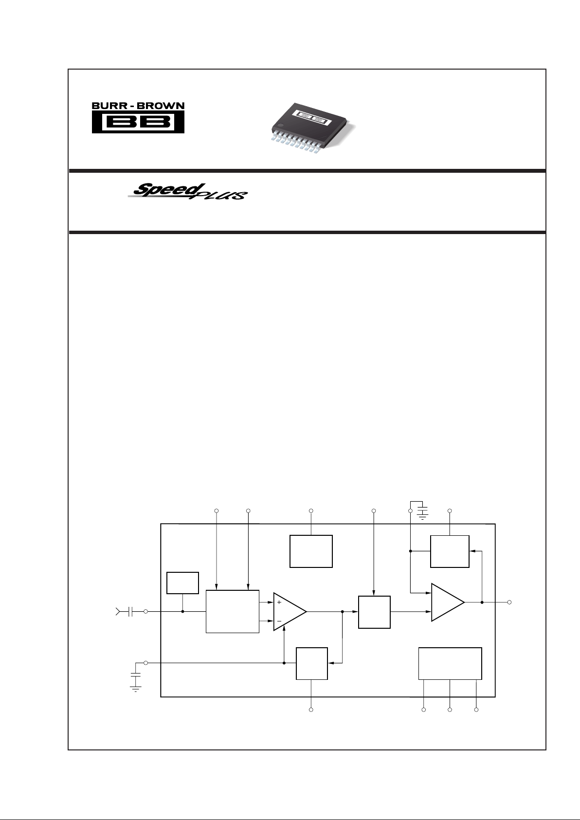
The VSP2080 is a complete front-end processing IC
for digital cameras. The VSP2080 provides signal
conditioning for the output of a CCD array. The
VSP2080 provides correlated double sampling to extract the video information from the pixels, 0dB to
+34dB gain range with analog control for varying
illumination conditions, and black level clamping for
an accurate black reference. The stable gain control is
linear in dB. Additionally, the black level quickly
recovers after screen changes. The MODE pin allows
the selection of logic-input polarity. The VSP2080 is
available in a 20-lead TSSOP package.
©
1998 Burr-Brown Corporation PDS-1498B Printed in U.S.A. August, 1999
TM
International Airport Industrial Park • Mailing Address: PO Box 11400, Tucson, AZ 85734 • Street Address: 6730 S. Tucson Blvd., Tucson, AZ 85706 • Tel: (520) 746-1111
Twx: 910-952-1111 • Internet: http://www.burr-brown.com/ • Cable: BBRCORP • Telex: 066-6491 • FAX: (520) 889-1510 • Immediate Product Info: (800) 548-6132
APPLICATIONS
● VIDEO CAMERAS
● DIGITAL STILL CAMERAS
● PC CAMERAS
● SECURITY CAMERAS
CCD R
CCD D
CCD
OUT
Optical
Black Level
Auto-Zero
Dummy
Pixel
Auto-Zero
+28dB
Log
VCA
Correlated
Double
Sampling
Clamp
+6dB
REFCK DATCK
AGC IN
C
DUMC
Internal
Bias
Generator
REFT REFB REF IN
Logic Input
Polarity
Control
MODE
OB
OUT
®
VSP2080

®
2
VSP2080
SPECIFICATIONS
At TA = +25°C, and V
DDA
= +3.0V, unless otherwise specified.
VSP2080T
PARAMETER CONDITIONS MIN TYP MAX UNITS
DIGITAL INPUT
Logic Family CMOS
Logic Levels Logic HI 2.5 +V
DDA
V
Logic LO 0 +0.4 V
Logic Currents Logic HI, V
IN
= +V
DDA
10 µA
Logic LO, VIN = 0V 10 µA
ANALOG OUTPUT
Output Voltage 1.0 2.0 V
Output Black Level 1.010 1.030 1.045 x REF IN
Reference Input (REF IN) 0.90 1.0 1.1 V
TRANSFER CHARACTERISTICS
Signal-to-Noise Ratio
(1)
Grounded Input Cap, 55 dB
Gain Min
Black Clamp Level 31 mV
CDS
Data Settling Time to ±0.1% for FS Change From Leading Edge 11 ns
with R
S
= 40 of DATCK
Input Capacitance DATCK LOW 20 pF
Input Time Constant 300 ps
Full-Scale Input Voltage After AC-Coupling Cap 600 mV
INPUT CLAMP
Clamp-On Resistance 3.3 kΩ
Clamp Level 1V
GAIN CONTROL CHARACTERISTICS
Linear Gain Control Voltage Range 0.7 2.3 V
Gain at Max Control Voltage 34 dB
Gain Control Linearity ±1.0 dB
Gain Control Settling Time 10 µs
Transfer Function Linear Range 20.6 dB /V
POWER SUPPLY
Rated Voltage +2.7 +3.0 +3.6 V
Current, Quiescent 48 mA
Power Dissipation 144 mW
Power-Down Mode 10 mW
TEMPERATURE RANGE
Specified Range Ambient –25 +85 °C
Thermal Resistance,
θ
JA
20-Lead TSSOP 130 °C/W
NOTE: (1) SNR = 20log (full-scale voltage / r ms noise).
The information provided herein is believed to be reliable; however, BURR-BROWN assumes no responsibility for inaccuracies or omissions. BURR-BROWN
assumes no responsibility for the use of this information, and all use of such information shall be entirely at the user’s own risk. Prices and specifications are subject
to change without notice. No patent rights or licenses to any of the circuits described herein are implied or granted to any third party. BURR-BROWN does not
authorize or warrant any BURR-BROWN product for use in life support devices and/or systems.
®
3
VSP2080
+VS....................................................................................................... +6V
Analog Input.......................................................... –0.3V to (+V
DDA
+0.3V)
Logic Input ............................................................ –0.3V to (+V
DDA
+0.3V)
Case Temperature ......................................................................... +100°C
Junction Temperature .................................................................... +150°C
Storage Temperature..................................................................... +150°C
ABSOLUTE MAXIMUM RATINGS
PIN DESIGNATOR TYPE DESCRIPTION
1 LCM Bypass Attenuator Common-Mode Bypass,
Bypass to GND with 0.1µF capacitor
2 2.4V Bypass Attenuator Ladder Bypass,
Bypass to GND with 0.1µF capacitor
3 OUT Analog Output Analog Output
4 C Capacitor Capacitor for Optical Black Auto-Zero
Loop
5 MODE Logic Input Mode Control for Logic Input:
LO = Positive Pulse Active
HI = Negative Pulse Active
6 OB Logic Input Optical Black Clamp Pulse
7 REFCK Logic Input Sampling Pulse for Reset
8 DATCK Logic Input Sampling Pulse for Data
9 DUMC Logic Input Dummy Pixel Clamp Pulse
10 PD Logic Input Power-Down Control:
LO = Normal Operation
HI = Reduced Power
11 V
DDA
Power Supply Positive Power Supply
12 GND
A
Ground Analog Ground
13 CCD D Analog Input CCD Signal Input
14 CCD R Capacitor Capacitor for Dummy Feedback Loop
15 GND
A
Ground Analog Ground
16 AGC IN Analog Input Sets Gain of Gain Control Amp.
17 V
DDA
Power Supply Positive Power Supply
18 REFT Bypass Bypass for Internal Top Reference
19 REFB Bypass Bypass for Internal Bottom Reference
20 REF IN Analog Input External Reference Input (1.0V)
PIN CONFIGURATION
PIN DESCRIPTIONS
Top View TSSOP
LCM
2.4V
OUT
C
MODE
OB
REFCK
DATCK
DUMC
PD
REF IN
REFB
REFT
V
DDA
AGC IN
GND
A
CCD R
CCD D
GND
A
V
DDA
1
2
3
4
5
6
7
8
9
10
20
19
18
17
16
15
14
13
12
11
VSP2080T
PACKAGE SPECIFIED
DRAWING TEMPERATURE PACKAGE ORDERING TRANSPORT
PRODUCT PACKAGE NUMBER
(1)
RANGE MARKING NUMBER
(2)
MEDIA
VSP2080T 20-Lead TSSOP 353 –25°C to +85°C VSP2080T VSP2080T 250-Piece Tray
" " " " " VSP2080T/2K Tape and Reel
NOTES: (1) For detailed drawing and dimension table, please see end of data sheet, or Appendix C of Burr-Brown IC Data Book. (2) Models with a slash (/ ) are
available only in Tape and Reel in the quantities indicated (e.g., /2K indicates 2000 devices per reel). Ordering 2000 pieces of “VSP2080T/2K” will get a single 2000piece Tape and Reel.
PACKAGE/ORDERING INFORMATION
ELECTROSTATIC
DISCHARGE SENSITIVITY
This integrated circuit can be damaged by ESD. Burr-Brown
recommends that all integrated circuits be handled with
appropriate precautions. Failure to observe proper handling
and installation procedures can cause damage.
ESD damage can range from subtle performance degradation
to complete device failure. Precision integrated circuits may
be more susceptible to damage because very small parametric
changes could cause the device not to meet its published
specifications.
 Loading...