


®
Voltage-to-Frequency
and Frequency-to-Voltage
CONVERTER
VFC32
FEA TURES
● OPERATION UP TO 500kHz
● EXCELLENT LINEARITY
±0.01% max at 10kHz FS
±0.05% max at 100kHz FS
● V/F OR F/V CONVERSION
● MONOTONIC
● VOLTAGE OR CURRENT INPUT
APPLICATIONS
● INTEGRATING A/D CONVERTER
● SERIAL FREQUENCY OUTPUT
● ISOLATED DATA TRANSMISSION
● FM ANALOG SIGNAL MOD/DEMOD
● MOTOR SPEED CONTROL
● TACHOMETER
V
OUT
Comparator
Input
DESCRIPTION
The VFC32 voltage-to-frequency converter provides
an output frequency accurately proportional to its
input voltage. The digital open-collector frequency
output is compatible with all common logic families.
Its integrating input characteristics give the VFC32
excellent noise immunity and low nonlinearity.
Full-scale output frequency is determined by an external capacitor and resistor and can be scaled over a
wide range. The VFC32 can also be configured as a
frequency-to-voltage converter.
The VFC32 is available in 14-pin plastic DIP, SO-14
surface-mount, and metal TO-100 packages. Commercial, industrial, and military temperature range models
are available.
+V
CC
f
–In
+In
–V
CC
International Airport Industrial Park • Mailing Address: PO Box 11400 • Tucson, AZ 85734 • Street Address: 6730 S. Tucson Blvd. • Tucson, AZ 85706
Tel: (602) 746-1111 • Twx: 910-952-1111 • Cable: BBRCORP • Telex: 066-6491 • FAX: (602) 889-1510 • Immediate Product Info: (800) 548-6132
©
1977 Burr-Brown Corporation PDS-372G Printed in U.S.A. October, 1998
One-Shot
VFC32
One-Shot
Capacitor
OUT
Common

SPECIFICATIONS
At T
= +25°C and V
A
PARAMETER CONDITIONS MIN TYP MAX MIN TYP MAX MIN TYP MAX UNITS
INPUT (V/F CONVERTER) F
Voltage Range
Positive Input >0 +0.25mA ✽✽✽✽V
Negative Input >0 –10 ✽✽✽✽V
Current Range
Bias Current
Inverting Input 20 100 ✽✽ ✽✽ nA
Noninverting Input 100 250 ✽✽ ✽✽ nA
Offset Voltage
Differential Impedance 300 || 10 650 || 10 ✽✽ ✽ ✽ kΩ || pF
Common-mode
Impedance 300 || 3 500 || 3 ✽✽ ✽✽ MΩ || pF
INPUT (F/V CONVERTER) V
Impedance 50 || 10 150 || 10 ✽✽ ✽✽ kΩ || pF
Logic “1” +1.0 ✽✽✽✽V
Logic “0” –0.05 ✽✽✽ ✽V
Pulse-width Range 0.1 150k/F
ACCURACY
Linearity Error
Offset Error Input
Offset Votlage
Offset Drift
Gain Error
Gain Drift
(6)
(2)
(6)
Full Scale Drift f = 10kHz ±75 ±50 ±100 ±70 ±150 ppm of FSR/°C
(offset drift and
(6, 7)
gain drift)
Power Supply f = DC, ±VCC = 12VDC
Sensitivity to 18VDC ±0.015 ✽✽% of FSR/%
OUTPUT (V/F CONVERTER) (open collector output)
Voltage, Logic “0” I
Leakage Current,
Logic “1” V
Voltage, Logic “1” External Pull-up Resistor
Pulse Width For Best Linearity 0.25/F
Fall Time I
OUTPUT (F/V CONVERTER) V
Voltage IO ≤ 7mA 0 to +10 ✽✽ V
Current V
Impedance Closed Loop 1 ✽✽Ω
Capacitive Load Without Oscillation 100 ✽✽pF
DYNAMIC RESPONSE
Full Scale Frequency 500
Dynamic Range 6 ✽✽ decades
Settling Time (V/F) to Specified Linearity
Overload Recovery < 50% Overload
POWER SUPPLY
Rated Voltage ±15 V
Voltage Range ±11 ±20 ✽ V
Quiescent Current ±5.5 ±6.0 ✽✽ ✽ mA
TEMPERATURE RANGE
Specification 0 +70 –25 +85 –55 +125 °C
Operating –25 +85 –55 +125 –55 +125 °C
Storage –25 +85 –65 +150 –65 +150 °C
= ±15V, unless otherwise noted.
CC
= VIN/7.5 R1 C
(1)
(1)
(2)
(3)
OUT
= 7.5 R1 C1 F
OUT
0.01Hz ≤ Oper
Freq ≤ 10kHz ±0.005 ±0.010
0.1Hz ≤ Oper
Freq ≤ 100kHz ±0.025 ±0.05 ✽✽ ✽✽% of FSR
0.5Hz ≤ Oper
Freq ≤ 500kHz ±0.05 ✽✽% of FSR
(2)
Required (see Figure 4) V
= 5mA, C
OUT
OUT
for a Full Scale Input Step
VFC32KP, KU VFC32BM VFC32SM
1
x R
1
>0 +0.25 ✽✽✽✽mA
14 ✽✽ ✽✽ mV
IN
✽✽✽✽µs
MAX
(4)
✽✽ ✽✽% of FSR
14 ✽✽ ✽✽ mV
±3 ✽✽ppm of FSR/°C
5 ✽✽% of FSR
f = 10kHz ±75 ±50 ±100 ±70 ±150 ppm/°C
= 8mA 0 0.2 0.4 ✽✽✽✽✽✽ V
SINK
= 15V 0.01 1.0 ✽✽ ✽✽ µA
O
PU
= 500pF 400 ✽✽ns
LOAD
≤ 7VDC +10 ✽✽ mA
O
MAX
(8)
✽✽ kHz
(9)
(9)
✽✽V
✽✽s
✽✽
✽✽
(5)
✽ Specification the same as VFC32KP.
NOTES: (1) A 25% duty cycle (0.25mA input current) is recommended for best linearity. (2) Adjustable to zero. See Offset and Gain Adjustment section. (3) Linearity error is specified
at any operating frequency from the straight line intersecting 90% of full scale frequency and 0.1% of full scale frequency. See Discussion of Specifications section. Above 200kHz,
it is recommended all grades be operated below +85°C. (4) ±0.015% of FSR for negative inputs shown in Figure 5. Positive inputs are shown in Figure 1. (5) FSR = Full Scale Range
(corresponds to full scale frequency and full scale input voltage). (6) Exclusive of external components’ drift. (7) Positive drift is defined to be increasing frequency with increasing
temperature. (8) For operations above 200kHz up to 500kHz, see Discussion of Specifications and Installation and Operation sections. (9) One pulse of new frequency plus 1µs.
2VFC32
ABSOLUTE MAXIMUM RATINGS
Supply Voltage................................................................................... ±22V
Output Sink Current (F
Output Current (V
Input Voltage, –Input..................................................................... ±Supply
Input Voltage, +Input..................................................................... ±Supply
Comparator Input .......................................................................... ±Supply
Storage Temperature Range:
VFC32BM, SM ............................................................. –65°C to +150°C
VFC32KP, KU ................................................................ –25°C to +85°C
) ................................................................ 50mA
OUT
) ...................................................................... +20mA
OUT
PACKAGE/ORDERING INFORMATION
PACKAGE
DRAWING TEMPERATURE
(1)
PRODUCT PACKAGE NUMBER
VFC32KP 14-Pin Plastic DIP 010 0°C to 70°C
VFC32BM TO-100 Metal 007 –25°C to +85°C
VFC32SM TO-100 Metal 007 –55°C to +125°C
VFC32KU SO-14 SOIC 235 0°C to +70°C
NOTE: (1) For detailed drawing and dimension table, please see end of data
sheet, or Appendix C of Burr-Brown IC Data Book.
RANGE
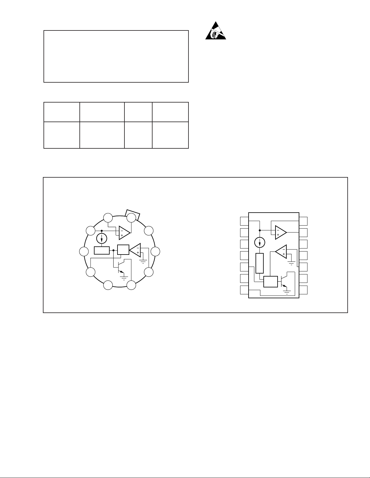
PIN CONFIGURATIONS
Top View
ELECTROSTATIC
DISCHARGE SENSITIVITY
This integrated circuit can be damaged by ESD. Burr-Brown
recommends that all integrated circuits be handled with
appropriate precautions. Failure to observe proper handling and
installation procedures can cause damage.
ESD damage can range from subtle performance degradation to
complete device failure. Precision integrated circuits may be
more susceptible to damage because very small parametric
changes could cause the device not to meet its published specifications.
–V
(Case)
CC
One-Shot
Capacitor
M Package
(TO-100)
+In
1
Input Amp
2
–In
Switch
3
4
56
NC
NC = no internal connection
External connection permitted.
One-
shot
P Package
U Package
V
OUT
10
+V
CC
9
Common
8
Comparator
7
Input
f
OUT
–In
NC
NC
–V
One-Shot
Capacitor
NC
f
OUT
CC
(Epoxy Dual-in-line)
1
2
3
4
5
6
7
Switch
One-
shot
Input
Amp
14
13
12
11
10
9
8
+In
V
OUT
+V
CC
Common
Comparator
Input
NC
NC
The information provided herein is believed to be reliable; however, BURR-BROWN assumes no responsibility for inaccuracies or omissions. BURR-BROWN assumes
no responsibility for the use of this information, and all use of such information shall be entirely at the user’s own risk. Prices and specifications are subject to change
without notice. No patent rights or licenses to any of the circuits described herein are implied or granted to any third party. BURR-BROWN does not authorize or warrant
any BURR-BROWN product for use in life support devices and/or systems.
3 VFC32
 Loading...