

Burr Brown VFC320BM, VFC320BG, VFC320SM, VFC320CM, VFC320CG Datasheet
®
Voltage-to-Frequency
and Frequency-to-Voltage
CONVERTER
VFC320
FEATURES
● HIGH LINEARITY, 12 to 14 bits
±0.005% max at 10kHz FS
±0.03% max at 100kHz FS
±0.1% typ at 1MHz FS
● V/F OR F/V CONVERSION
● 6-DECADE DYNAMIC RANGE
● 20ppm/
● OUTPUT TTL/CMOS COMPATIBLE
°C max GAIN DRIFT
APPLICATIONS
● INEXPENSIVE A/D AND D/A CONVERTER
● DIGITAL PANEL METERS
● TWO-WIRE DIGITAL TRANSMISSION
WITH NOISE IMMUNITY
● FM MOD/DEMOD OF TRANSDUCER
SIGNALS
● PRECISION LONG TERM INTEGRATOR
● HIGH RESOLUTION OPTICAL LINK FOR
ISOLATION
● AC LINE FREQUENCY MONITOR
● MOTOR SPEED MONITOR AND CONTROL
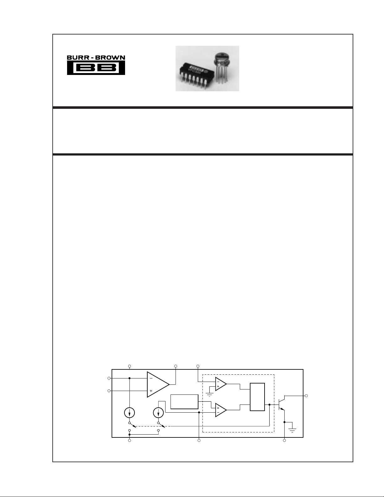
DESCRIPTION
The VFC320 monolithic voltage-to-frequency and frequency-to-voltage converter provides a simple low
cost method of converting analog signals into digital
pulses. The digital output is an open collector and the
digital pulse train repetition rate is proportional to the
amplitude of the analog input voltage. Output pulses
are compatible with TTL, and CMOS logic families.
High linearity (0.005%, max at 10kHz FS) is achieved
with relatively few external components. Two external resistors and two external capacitors are required
to operate. Full scale frequency and input voltage are
determined by a resistor in series with –In and two
capacitors (one-shot timing and input amplifier integration). The other resistor is a non-critical open
collector pull-up (f
able in three performance/temperature grades and two
package configurations. The TO-100 versions are hermetically sealed, and specified for the –25°C to +85°C
and –55°C to +125°C ranges, and the dual-in-line
units are specified from –25°C to +85°C.
to +VCC). The VFC320 is avail-
OUT
+V
CC
–In
+In
–V
CC
International Airport Industrial Park • Mailing Address: PO Box 11400, Tucson, AZ 85734 • Street Address: 6730 S. Tucson Blvd., Tucson, AZ 85706 • Tel: (520) 746-1111 • Twx: 910-952-1111
Internet: http://www.burr-brown.com/ • FAXLine: (800) 548-6133 (US/Canada Only) • Cable: BBRCORP • Telex: 066-6491 • FAX: (520) 889-1510 • Immediate Product Info: (800) 548-6132
©
1982 Burr-Brown Corporation PDS-483J Printed in U.S.A. August, 1993
V
OUT
–7.5V Ref
f
IN
C
1
Comparators
One-shot
Flip-
flop
Common
f
OUT
SPECIFICATIONS
At TA = +25°C and ±15VDC power supply, unless otherwise noted.
VFC320BG/BM/SM VFC320CG/CM
PARAMETER CONDITIONS MIN TYP MAX MIN TYP MAX UNITS
V/F CONVERTER f
INPUT TO OP AMP
Voltage Range
Current Range
Bias Current
Inverting Input 48 ✻✻ nA
Noninverting Input 10 30 ✻✻ nA
Offset Voltage
Offset Voltage Drift ±5 ✻ µV/°C
Differential Impedance 300 || 5 650 || 5 ✻✻ kΩ || pF
Common-Mode
Impedance 300 || 3 500 || 3 ✻✻ kΩ || pF
ACCURACY
Linearity Error
Offset Error Input
Offset Voltage
Offset Drift
Gain Error
Gain Drift
(7)
(3)
(7)
Full Scale Drift f = 10kHz 50 20 ppm FSR/°C
(Offset Drift and Gain Drift)
Power Supply Sensitivity ±VCC = 14VDC to 18VDC ±0.015 ✻ % FSR%
DYNAMIC RESPONSE
Full Scale Frequency C
Dynamic Range 6 ✻ Decades
Settling Time (V/F) to Specified Linearity
Overload Recovery <50% Overload Note 10 ✻
OPEN COLLECTOR OUTPUT
Voltage, Logic “0” I
Leakage Current, Logic “1” V
Voltage, Logic “1” External Pull-up Resistor
Duty Cycle at FS For Best Linearity 25 ✻ %
Fall Time I
F/V CONVERTER V
INPUT TO COMPARATOR
Impedance 50 || 10 150 || 10 ✻✻ kΩ || pF
Logic “1” +1.0 +V
Logic “0” –V
Pulse-width Range 0.25 ✻ µs
OUTPUT FROM OP AMP
Voltage I
Current V
Impedance Closed-Loop 0.1 ✻ Ω
Capacitive Load Without Oscillation 100 ✻ pF
POWER SUPPLY
Rated Voltage ±15 ✻ V
Voltage Range ±13 ±20 ✻✻V
Quiescent Current ±6.5 ±7.5 ✻✻ mA
TEMPERATURE RANGE
Specification
B and C Grades –25 +85 ✻✻°C
S Grade –55 +125 °C
Operating
B and C Grades –40 +85 ✻✻°C
S Grade –55 +125 °C
Storage –65 +150 ✻✻°C
✻
Specification the same as for VFC320BG/BM/SM.
NOTES: (1) A 25% duty cycle at full scale (0.25mA input current) is recommended where possible to achieve best linearity. (2) Determined by RIN and full scale current range
constraints. (3) Adjustable to zero. See Offset and Gain Adjustment section. (4) Linearity error at any operating frequency is defined as the deviation from a straight line drawn between
the full scale frequency and 0.1% of full scale frequency. See Discussion of Specifications section. (5) When offset and gain errors are nulled, at an operating temperature, the linearity
error determines the final accuracy. (6) For e
(8) FSR = Full Scale Range (corresponds to full scale and full scale input voltage.) (9) Positive drift is defined to be increasing frequency with increasing temperature.
(10) One pulse of new frequency plus 50ns typical.
= VIN/ 7.5 R1C1, Figure 4
OUT
(1)
(1)
(3)
(1) (4) (5)
(3)
= 7.5 R1C1 fIN, Figure 9
OUT
®
VFC320
(7)(8)(9)
Fig. 4 with e2 = 0 >0 Note 2 V
Fig. 4 with e
IIN = VIN/R
= 0 <0 –10 V
1
IN
+0.25 +750 ✻✻µA
±0.15 ✻ mV
Fig. 4 with e2 = 0
0.01Hz ≤ f
0.1Hz ≤ f
1Hz ≤ f
(6)
≤ 10kHz ±0.004 ±0.005 ±0.0015 ±0.002 % FSR
OUT
≤ 100kHz ±0.008 ±0.030 ✻✻% FSR
OUT
≤ 1MHz ±0.1 ✻ % FSR
OUT
±15 ✻ ppm FSR
±0.5 ✻ ppm FSR/°C
±5 ±10 ✻✻% FSR
f = 10kHz 50 20 ppm FSR/°C
≤ 50pF 1 ✻ MHz
LOAD
For a Full Scale Input Step Note 10 ✻
= 8mA, max 0.4 ✻ V
SINK
= 15V 0.01 1.0 ✻✻ µA
O
Required (See Figure 4) V
= 5mA, C
OUT
= 0 typical linearity errors are: 0.01% at 10kHz, 0.2% at 100kHz, 0.1% at 1MHz. (7) Exclusive of external components’ drift.
1
= 500pF 100 ✻ ns
LOAD
CC
= 6mA 0 to +10 ✻ V
O
= 7VDC +10 ✻ mA
O
PU
CC
–0.05 ✻✻V
✻✻V
✻ V
2
CONNECTION DIAGRAM
Top View TO-100 Top View DIP
+In
1
2
–In
Switch
3
(Case)
–V
CC
One-Shot
Capacitor
4
56
NC
NC = no internal connection
External connection permitted.
Input Amp
One-
shot
V
OUT
10
f
OUT
+V
CC
9
Common
8
Comparator
7
Input
–In
NC
NC
–V
One-Shot
Capacitor
NC
f
OUT
1
2
3
4
CC
5
Switch
6
7
One-
shot
Input
Amp
14
13
12
11
10
9
8
+In
V
OUT
+V
CC
Common
Comparator
Input
NC
NC
PACKAGE/ORDERING INFORMATION
PACKAGE
DRAWING TEMPERATURE
PRODUCT PACKAGE NUMBER
VFC320BG 14-Pin Ceramic DIP 163 –40°C to +85°C
VFC320BM TO-100 007 –40°C to +85°C
VFC320SM TO-100 007 –40°C to +85°C
VFC320CG 14-Pin Ceramic DIP 163 –40°C to +85°C
VFC320CM TO-100 007 –40°C to +85°C
NOTE: (1) For detailed drawing and dimension table, please see end of data
sheet, or Appendix C of Burr-Brown IC Data Book.
(1)
RANGE
ABSOLUTE MAXIMUM RATINGS
Supply Voltage ................................................................................... ±20V
Output Sink Current at f
Output Current at V
Input Voltage, –Input .......................................................................... ±V
Input Voltage, +Input.......................................................................... ±V
Storage Temperature Range .......................................... –65°C to +150°C
Lead Temperature (soldering, 10s)................................................ +300°C
...............................................................50mA
OUT
...................................................................+20mA
OUT
CC
CC
ELECTROSTATIC
DISCHARGE SENSITIVITY
This integrated circuit can be damaged by ESD. Burr-Brown
recommends that all integrated circuits be handled with
appropriate precautions. Failure to observe proper handling
and installation procedures can cause damage.
ESD damage can range from subtle performance degradation
to complete device failure. Precision integrated circuits may
be more susceptible to damage because very small parametric
changes could cause the device not to meet its published
specifications.
The information provided herein is believed to be reliable; however, BURR-BROWN assumes no responsibility for inaccuracies or omissions. BURR-BROWN assumes no responsibility
for the use of this information, and all use of such information shall be entirely at the user’s own risk. Prices and specifications are subject to change without notice. No patent rights or
licenses to any of the circuits described herein are implied or granted to any third party. BURR-BROWN does not authorize or warrant any BURR-BROWN product for use in life support
devices and/or systems.
®
3
VFC320
 Loading...