

Burr Brown VFC110BG, VFC110SG, VFC110AG Datasheet
®
VFC110
High-Frequency
VOLTAGE-TO-FREQUENCY CONVERTER
FEATURES
● HIGH-FREQUENCY OPERATION:
4MHz FS max
● EXCELLENT LINEARITY:
±0.02% typ at 2MHz
● PRECISION 5V REFERENCE
● DISABLE PIN
● LOW JITTER
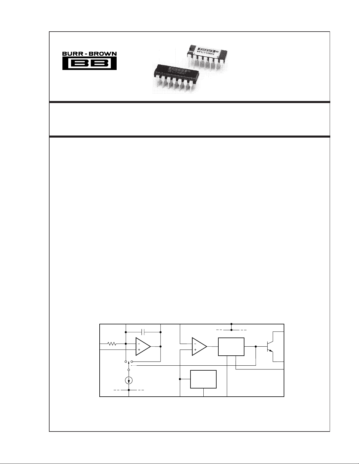
DESCRIPTION
The VFC110 voltage-to-frequency converter is a thirdgeneration VFC offering improved features and performance. These include higher frequency operation,
an on-board precision 5V reference and a Disable
function.
The precision 5V reference can be used for offsetting
the VFC transfer function, as well as exciting transducers or bridges. The Enable pin allows several
VFCs’ outputs to be paralleled, multiplexed, or simply
to shut off the VFC. The open-collector frequency
I
IN
112
V
OUT
Comparator
11
APPLICATIONS
● INTEGRATING A/D CONVERSION
● PROCESS CONTROL
● VOLTAGE ISOLATION
● VOLTAGE-CONTROLLED OSCILLATOR
● FM TELEMETRY
output is TTL/CMOS-compatible. The output may be
isolated by using an opto-coupler or transformer.
Internal input resistor, one-shot and integrator capacitors simplify applications circuits. These components
are trimmed for a full-scale output frequency of 4MHz
at 10V input. No additional components are required
for many applications.
The VFC110 is packaged in plastic and ceramic
14-pin DIPs. Industrial and military temperature range
gradeouts are available.
+V
S
10
f
8
OUT
V
2
Input Common
International Airport Industrial Park • Mailing Address: PO Box 11400, Tucson, AZ 85734 • Street Address: 6730 S. Tucson Blvd., Tucson, AZ 85706 • Tel: (520) 746-1111 • Twx: 910-952-1111
Internet: http://www.burr-brown.com/ • FAXLine: (800) 548-6133 (US/Canada Only) • Cable: BBRCORP • Telex: 066-6491 • FAX: (520) 889-1510 • Immediate Product Info: (800) 548-6132
© 1988 Burr-Brown Corporation PDS-861B Printed in U.S.A. October, 1993
IN
14
V
REF
413
–V
S
Analog Ground
PDS-861B
3
5V
One-Shot
6
C
OS
Digital Ground
7
Enable
5
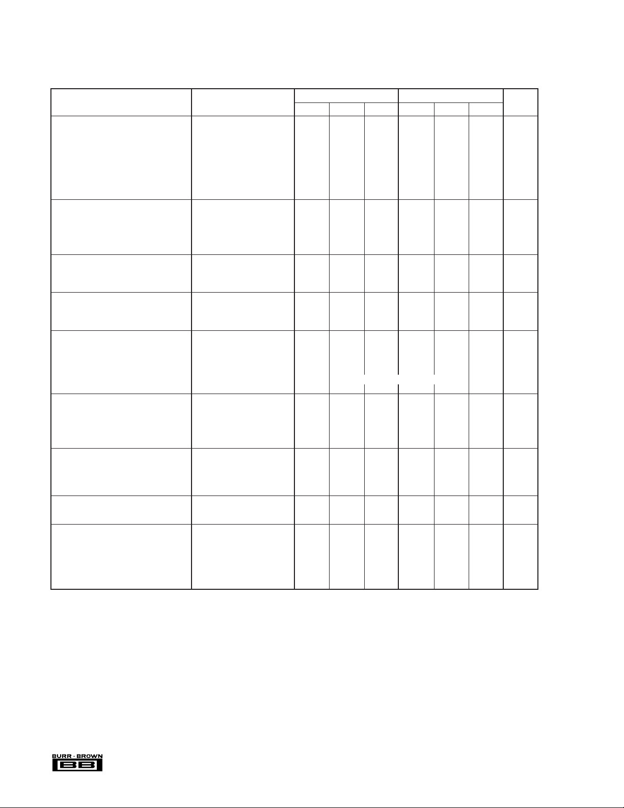
SPECIFICATIONS
At TA = +25°C and VS = ±15V, unless otherwise noted.
VFC110BG VFC110AG/SG/AP
PARAMETER CONDITIONS MIN TYP MAX MIN TYP MAX UNITS
VOLTAGE-TO-FREQUENCY OPERATION
Nonlinearity
Gain Error, f = 1MHz C
Gain Drift, f = 1MHz Specified Temp Range 50 100 ppm/°C
PSRR V
INPUT
Full Scale Input Current 250 500 * * µA
I
B
I
B
V
OS
V
OS
INTEGRATOR AMPLIFIER OUTPUT
Output Voltage Range R
Output Current Drive 5 20 * * mA
Capacitive Load No Oscillations 10 10 nF
COMPARATOR INPUT
I
B
Trigger Voltage ±50 * mV
Input Voltage Range –5 +V
OPEN COLLECTOR OUTPUT
V
O
I
LEAKAGE
Fall Time 25 * ns
Delay to Rise 25 * ns
Settling Time To Specified Linearity for a One Pulse of New Frequency Plus 1µs
REFERENCE VOLTAGE
Voltage 4.97 5 5.03 * * * V
Voltage Drift 20 50 ppm/°C
Load Regulation I
PSRR V
Current Limit Short Circuit 15 20 * mA
ENABLE INPUT
V
HIGH
V
LOW (fOUT
I
HIGH
I
LOW
POWER SUPPLY
Voltage, ±V
Current 13 16 * * mA
TEMPERATURE RANGE
Specified
Storage
* Same specifications as VFC110BG.
NOTE: (1) Nonlinearity measured from 1V to 10V input.
(1)
: f
= 100kHz COS = 2.2nF, RIN = 44kΩ 0.005 0.01 0.01 0.05 %FS
FS
f
= 1MHz COS = 150pF, RIN = 40kΩ 0.01 0.05 0.1 %FS
FS
f
= 2MHz COS = 56pF, RIN = 34kΩ 0.02 * %FS
FS
f
= 4MHz COS = (Int), RIN = (Int) 1 * %FS
Relative to V
FS
REF
= 150pF, RIN = 40kΩ 5*%
OS
Specified Temp Range 50 100 ppm/°C
= ±8V to ±18V 0.05 0.1 %/V
S
– (Inverting Input) 15 60 20 100 nA
+ (Non-Inverting Input) 250 * nA
33mV
Drift Specified Temp Range 35 * µV/°C
= 2kΩ –0.2 +VS – 4 * * V
L
(Input Bias Current) –5 * µA
S
**V
Low 0.4 * V
0.1 1 * * µA
Full-Scale Input Step
= 0 to 10mA 2 10 * * mV
O
= ±8V to ±18V 5 * mV/V
S
(f
Enabled) Specified Temp Range 2 * V
OUT
Disabled) Specified Temp Range 0.4 * V
0.1 * µA
1*µA
S
±8 ±15 ±18 * * * V
AG, BG, AP –25 +85 * * °C
SG –55 +125 °C
AG, BG, SG –65 +150 * * °C
AP –40 +125 * * °C
The information provided herein is believed to be reliable; however, BURR-BROWN assumes no responsibility for inaccuracies or omissions. BURR-BROWN assumes
no responsibility for the use of this information, and all use of such information shall be entirely at the user’s own risk. Prices and specifications are subject to change
without notice. No patent rights or licenses to any of the circuits described herein are implied or granted to any third party. BURR-BROWN does not authorize or warrant
any BURR-BROWN product for use in life support devices and/or systems.
®
VFC110
2
PIN CONFIGURATION ABSOLUTE MAXIMUM RATINGS
Top View DIP
V
+5V
Out
REF
–V
Enable
C
Digital Ground
1
I
IN
2
IN
3
4
S
5
6
OS
7
14
Input Common
13
Analog Common
12
V
OUT
11
Comparator In
10
+V
S
9
NC
8
f
OUT
Power Supply Voltages (+V
f
Sink Current............................................................................50mA
OUT
Comparator In Voltage .......................................................... –5V to +V
Enable Input........................................................................... +VS to –V
Integrator Common-Mode Voltage.................................. –1.5V to +1.5V
Integrator Differential Input Voltage ................................ +0.5V to –0.5V
Integrator Out (short-circuit)..................................................... Indefinite
V
Out (short-circuit)..............................................................Indefinite
REF
Operating Temperature Range
G Package ................................................................ –55°C to +125°C
P Package................................................................... –40°C to +85°C
Storage Temperature
G Package ................................................................ –60°C to +150°C
P Package................................................................. –40°C to +125°C
Lead Temperature (soldering, 10s)............................................. +300°C
to –VS) ................................................40V
S
PACKAGE INFORMATION
PRODUCT PACKAGE NUMBER
PACKAGE DRAWING
VFC110AG 14-Pin Ceramic DIP 169
VFC110BG 14-Pin Ceramic DIP 169
VFC110SG 14-Pin Ceramic DIP 169
VFC110AP 14-Pin Plastic DIP 010
NOTE: (1) For detailed drawing and dimension table, please see end of data
sheet, or Appendix D of Burr-Brown IC Data Book.
(1)
ORDERING INFORMATION
S
S
PRODUCT PACKAGE RANGE
TEMPERATURE
VFC110AG Ceramic DIP –25°C to +85°C
VFC110BG Ceramic DIP –25°C to +85°C
VFC110SG Ceramic DIP –55 °C to +125°C
VFC110AP Plastic DIP –25°C to +85°C
®
3
VFC110
 Loading...