

Burr Brown VFC100BG, VFC100AG Datasheet

®
VFC100
FPO
Synchronized
VOLTAGE-TO-FREQUENCY CONVERTER
FEATURES
● FULL-SCALE FREQUENCY SET BY
SYSTEM CLOCK; NO CRITICAL
EXTERNAL COMPONENTS REQUIRED
● PRECISION 10V FULL-SCALE INPUT,
0.5% max GAIN ERROR
● ACCURATE 5V REFERENCE VOLTAGE
● EXCELLENT LINEARITY:
0.02% max at 100kHz FS
0.1% max at 1MHz FS
● VERY LOW GAIN DRIFT: 50ppm/
°C
APPLICATIONS
● A/D CONVERSION
● PROCESS CONTROL
● DATA ACQUISITION
● VOLTAGE ISOLATION
V
OUT
– Comparator
Input
V
Non-Inverting
Input
C
INT
54
Integrator
Ω
SW
Amplifier
1
R
IN
7
IN
6
20k
14
Comparator
DESCRIPTION
The VFC100 voltage-to-frequency converter is an
important advance in VFCs. The well-proven charge
balance technique is used; however, the critical reset
integration period is derived from an external clock
frequency. The external clock accurately sets an output full-scale frequency, eliminating error and drift
from the external timing components required for
other VFCs. A precision input resistor is provided
which accurately sets a 10V full-scale input voltage.
In many applications the required accuracy can be
achieved without external adjustment.
The open collector active-low output provides fast fall
time on the important leading edge of output pulses,
and interfaces easily with TTL and CMOS circuitry.
An output one-shot circuit is particularly useful to
provide optimum output pulse widths for optical couplers and transformers to achieve voltage isolation. An
accurate 5V reference is also provided which is useful
for applications such as offsetting for bipolar input
voltages, exciting bridges and sensors, and autocalibration schemes.
Clock
Input
10
Clocked
Logic
+V
CC
1
Output
One-Shot
11
12
f
OUT
Digital
Common
1mA
–V
CC
13
Analog
Common
International Airport Industrial Park • Mailing Address: PO Box 11400, Tucson, AZ 85734 • Street Address: 6730 S. Tucson Blvd., Tucson, AZ 85706 • Tel: (520) 746-1111 • Twx: 910-952-1111
Internet: http://www.burr-brown.com/ • FAXLine: (800) 548-6133 (US/Canada Only) • Cable: BBRCORP • Telex: 066-6491 • FAX: (520) 889-1510 • Immediate Product Info: (800) 548-6132
© 1984 Burr-Brown Corporation PDS-547H Printed in U.S.A. June, 1995
15
+ Comparator
Input
5V
Reference
16
V
REF
9
C
OS
–V
8
CC
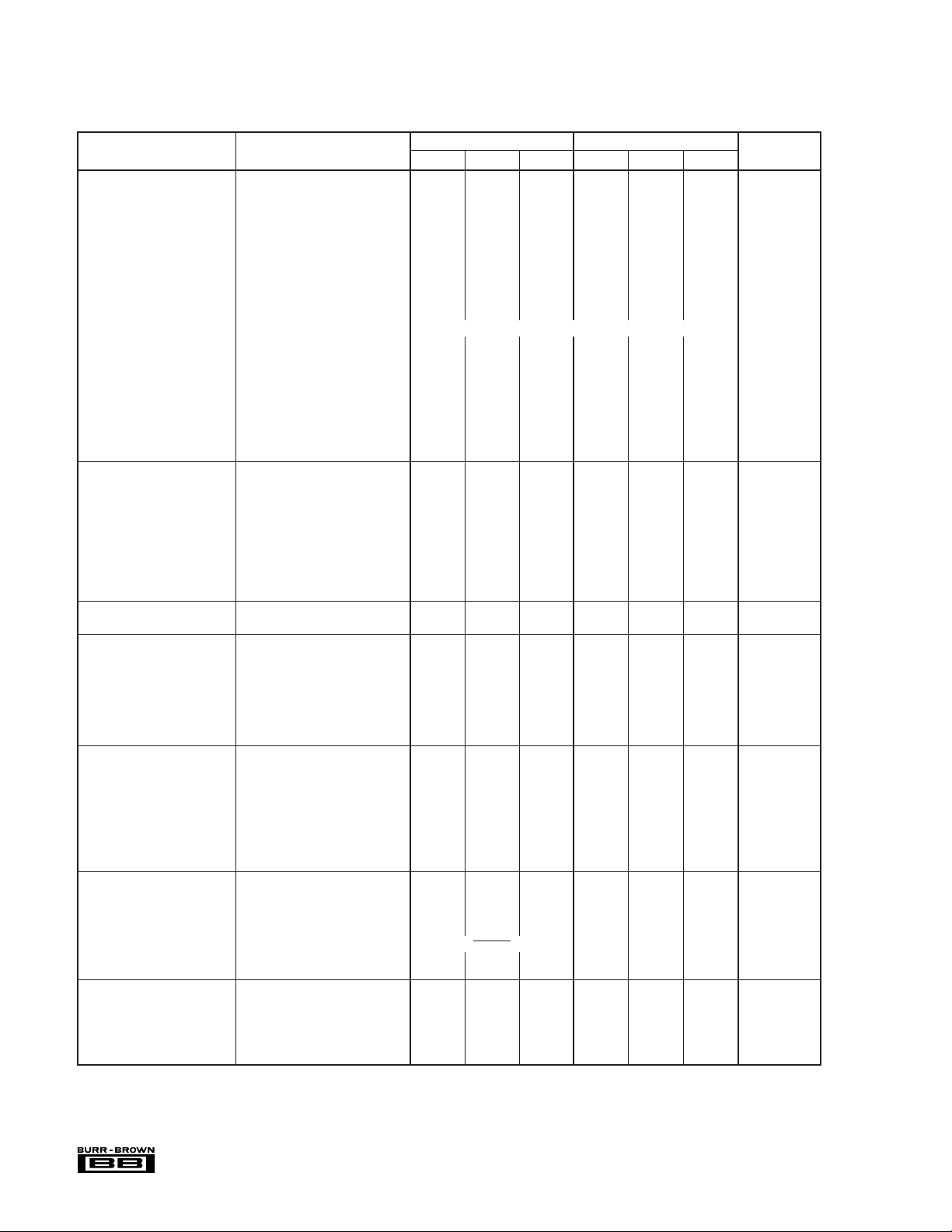
SPECIFICATIONS
At TA = +25°C and ±15VDC supplies, unless otherwise noted.
VFC100AG VFC100BG
PARAMETER CONDITIONS MIN TYP MAX MIN TYP MAX UNITS
TRANSFER FUNCTION
Voltage-to-Frequency Mode f
Gain Error
(1)
Linearity Error FSR = 100kHz, Over Temperature ±0.01 ±0.025 ✻ ±0.02 % of FSR
(2)
Gain Drift
Referred to Internal V
Offset Referred to Input ±1 ±3 ±1 ±2mV
REF
Offset Drift ±12 ±100 ±6.5 ±25 µV/°C
Power Supply Rejection Full Supply Range 0.01 ✻ %/V
Response Time To Step Input Change One Period of New Output Frequency Plus One Clock Period
Current-to-Frequency Mode f
Gain Error ±0.5 ±1 ±0.2 ±0.5 % of FSR
(2)
Gain Drift
Frequency-to-Voltage Mode
Gain Accuracy
(1)
(3)
Linearity FSR = 100kHz ±0.01 ±0.025 ✻ ±0.02 %
Input Resistor (R
Resistance 19.8 20 20.2 ✻✻✻ kΩ
Temperature Coefficient (TC)
INTEGRATOR OP AMP
(1)
V
OS
V
Drift ±5 ✻ µV/°C
OS
I
B
I
OS
A
OL
CMRR 80 105 ✻✻ dBV
)
IN
(2)
CM Range –7.5 +0.1 ✻✻V
V
Range Z
OUT
Bandwidth 14 ✻ MHz
COMPARATOR INPUTS
Input Current (Operating) –11V < V
CLOCK INPUT
(Referred to Digital Common)
Frequency (Maximum Operating)
Threshold Voltage 1.4 ✻ V
Voltage Range (Operating)
Input Current –V
Rise Time 2 ✻ µs
OPEN COLLECTOR OUTPUT
(Referred to Digital Common)
V
OL
I
OL
I
(Off Leakage) VOH = 30V 0.01 10 ✻✻ µA
OH
Delay Time, Positive Clock
Edge to Output Pulse 300 ✻ ns
Fall Time 100 ✻ ns
Output Capacitance 5 ✻ pF
OUTPUT ONE-SHOT
(6)
Active
Pulse Width Out COS = 300pF 1 1.4 2 ✻✻✻ µs
Deactivated
(5)
Pulse Width Out 100kHz ≤ FSR < 1MHz 1 ✻ sec
Pulse Width Out FSR = 1MHz 250 450 500 ✻✻✻ ns
REFERENCE VOLTAGE
Accuracy No Load 4.9 5 5.1 4.95 ✻ 5.05 V
(2)
Drift
Current Output Sourcing Capability 10 ✻ mA
Power Supply Rejection 0.015 0.015 %/V
Output Impedance 0.5 2 ✻✻ Ω
= f
OUT
FSR = 500kHz, C
FSR = 1MHz, C
OUT
V
OUT
x (VIN/20V)
CLOCK
FSR = 100kHz ±0.5 ±1 ±0.2 ±0.5 % of FSR
= 60pF ±0.015 ✻ ±0.05 % of FSR
OS
= 60pF ±0.025 ✻ ±0.1 % of FSR
FSR = 100kHz ±70 ±100 ±30 ±50
= f
FSR = 100kHz ±0.5 ±1 ±0.2 ±0.5 %
OS
x (IIN/1mA)
CLOCK
= 20V x (fIN/f
CLOCK
±70 ±100 ±30 ±50
±120 ±200 ±80 ±140
ppm of FSR/°C
ppm of FSR/°C
)
ppm of FSR/°C
(4)
±50 ±100 ✻✻ ppm°C
±150 ±1000 ✻✻ µV
±50 ±100 ±25 ±50 nA
100 200 50 100 nA
Z
= 5kΩ/10,000pF 100 120 ✻✻ dB
LOAD
= 5kΩ/10,000pF –0.2 +12 ✻✻ V
LOAD
COMPARATOR
< +VCC – 2V 5 ✻ µA
4 ✻ MHz
Over Temperature 0.8 2 ✻✻V
CC
< +V
CLOCK
I
= 10mA 0.4 ✻ V
OUT
CC
0.5 5 ✻✻ µA
4 f
CLOCK
< V
–VCC + 2V
+V
CC
✻✻V
15 ✻ mA
±60 ±150 ±40 ±100 ppm/°C
®
VFC100
2
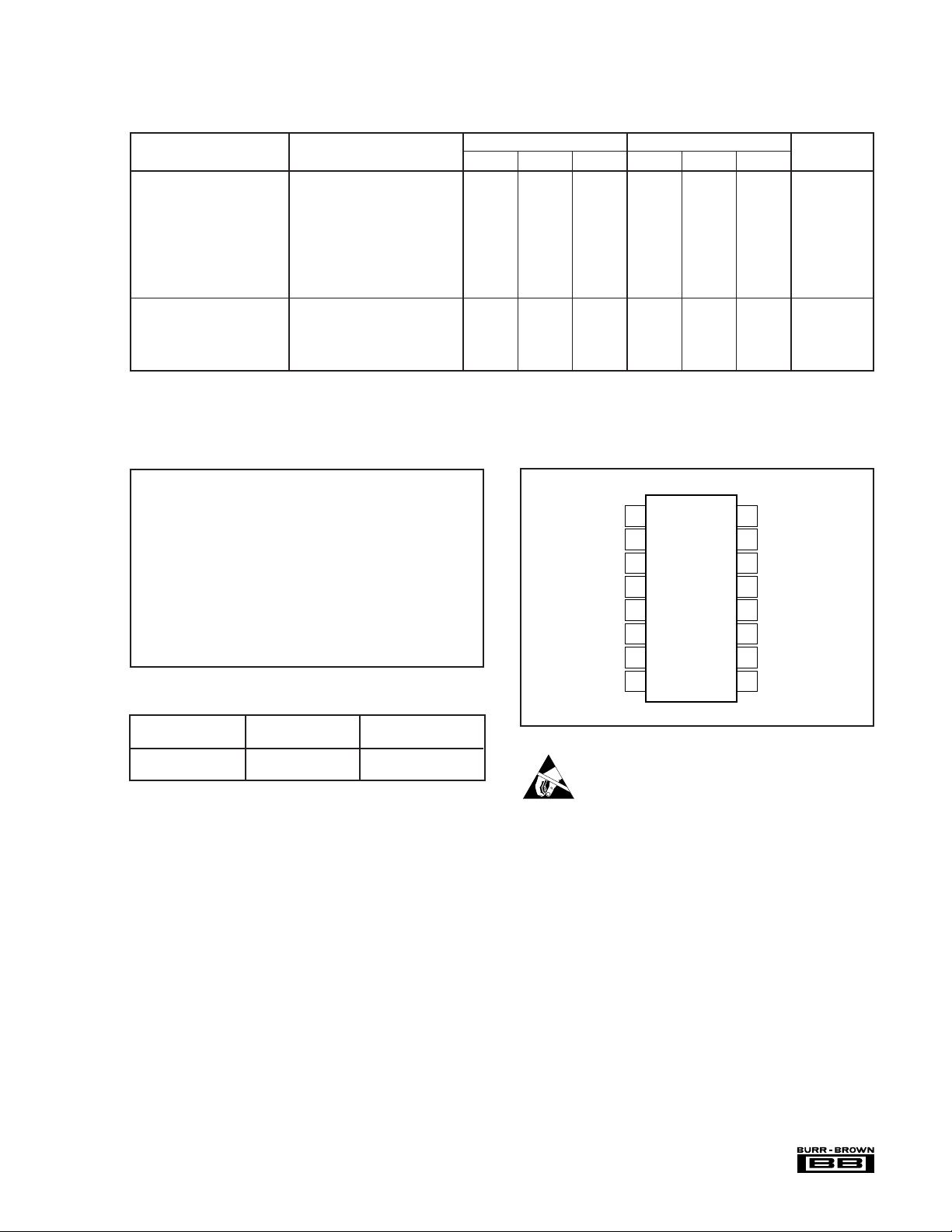
SPECIFICATIONS (CONT)
At TA = +25°C and ±15VDC supplies, unless otherwise noted.
VFC100AG VFC100BG
PARAMETER CONDITIONS MIN TYP MAX MIN TYP MAX UNITS
POWER SUPPLY
Rated Voltage ±15 ✻ V
Operating Voltage Range
(See Figure 9) +V
Total Supply +V
Digital Common –V
Quiescent Current: +I
TEMPERATURE RANGE
Specification –25 +85 ✻✻°C
Storage –65 +150 ✻✻°C
θ
JA
θ
JC
✻ Specification same as AG grade.
NOTES: (1) Offset and gain error can be trimmed to zero. See text. (2) Specified by the box method: (max. – min.) ÷ (FSR x ∆T). (3) Refer to detailed timing diagram
in Figure 16 for frequency input signal timing requirements. (4) FSR = Full Scale Range. (5) Pin 9 connected to +V
CC
–I
CC
CC
–V
CC
– (–VCC)15 36✻✻V
CC
Over Temperature 10.6 15 ✻✻ mA
+7.5 +28.5 ✻✻V
–7.5 –28.5 ✻✻V
+ 2 +VCC – 4 ✻✻V
CC
9.6 15 ✻✻ mA
150 ✻ °C/W
100 ✻ °C/W
. (6) Nominal PW
CC
= (5ns/pF) x COS – 90ns.
OUT
ABSOLUTE MAXIMUM RATINGS
Power Supply Voltage (+VCC to –V
+V
to Analog Common..................................................................... 28V
CC
–V
to Analog Common ..................................................................... 28V
CC
Integrator Out Short-Circuit to Ground ........................................ Indefinite
Integrator Differential Input ................................................................±10V
Integrator Common-Mode Input .................................... –V
V
(pin 7) ......................................................................................... ±V
IN
Clock Input......................................................................................... ±V
V
Out Short-Circuit to Ground ................................................ Indefinite
REF
Pin 9 (C
f
Digital Common ................................................................................. ±V
Storage Temperature Range .......................................... –65°C to +150°C
Lead Temperature (soldering, 10s) ................................................. 300°C
) .................................................................................0 to +V
OS
(referred to digital common).......................................... –0.5V to 36V
OUT
) ............................................... 36V
CC
+5V to +2V
CC
CC
CC
CC
CC
PACKAGE INFORMATION
PRODUCT PACKAGE NUMBER
PACKAGE DRAWING
VFC100AG 16-Pin Ceramic DIP 129
VFC100BG 16-Pin Ceramic DIP 129
NOTE: (1) For detailed drawing and dimension table, please see end of data
sheet, or Appendix C of Burr-Brown IC Data Book.
(1)
PIN CONFIGURATION
Top View DIP
+V
NC
NC
Integrator Out
C
Noninverting In
V
–V
1
CC
2
3
4
5
INT
6
7
IN
8
CC
16
V
15
+ Comparator In
14
– Comparator In
13
Analog Common
12
Digital Common
11
f
10
Clock Input
9
C
REF
OUT
OS
ELECTROSTATIC
DISCHARGE SENSITIVITY
This integrated circuit can be damaged by ESD. Burr-Brown
recommends that all integrated circuits be handled with
appropriate precautions. Failure to observe proper handling
and installation procedures can cause damage.
ESD damage can range from subtle performance degradation
to complete device failure. Precision integrated circuits may
be more susceptible to damage because very small parametric
changes could cause the device not to meet its published
specifications.
The information provided herein is believed to be reliable; however, BURR-BROWN assumes no responsibility for inaccuracies or omissions. BURR-BROWN assumes
no responsibility for the use of this information, and all use of such information shall be entirely at the user’s own risk. Prices and specifications are subject to change
without notice. No patent rights or licenses to any of the circuits described herein are implied or granted to any third party. BURR-BROWN does not authorize or warrant
any BURR-BROWN product for use in life support devices and/or systems.
3
VFC100
®
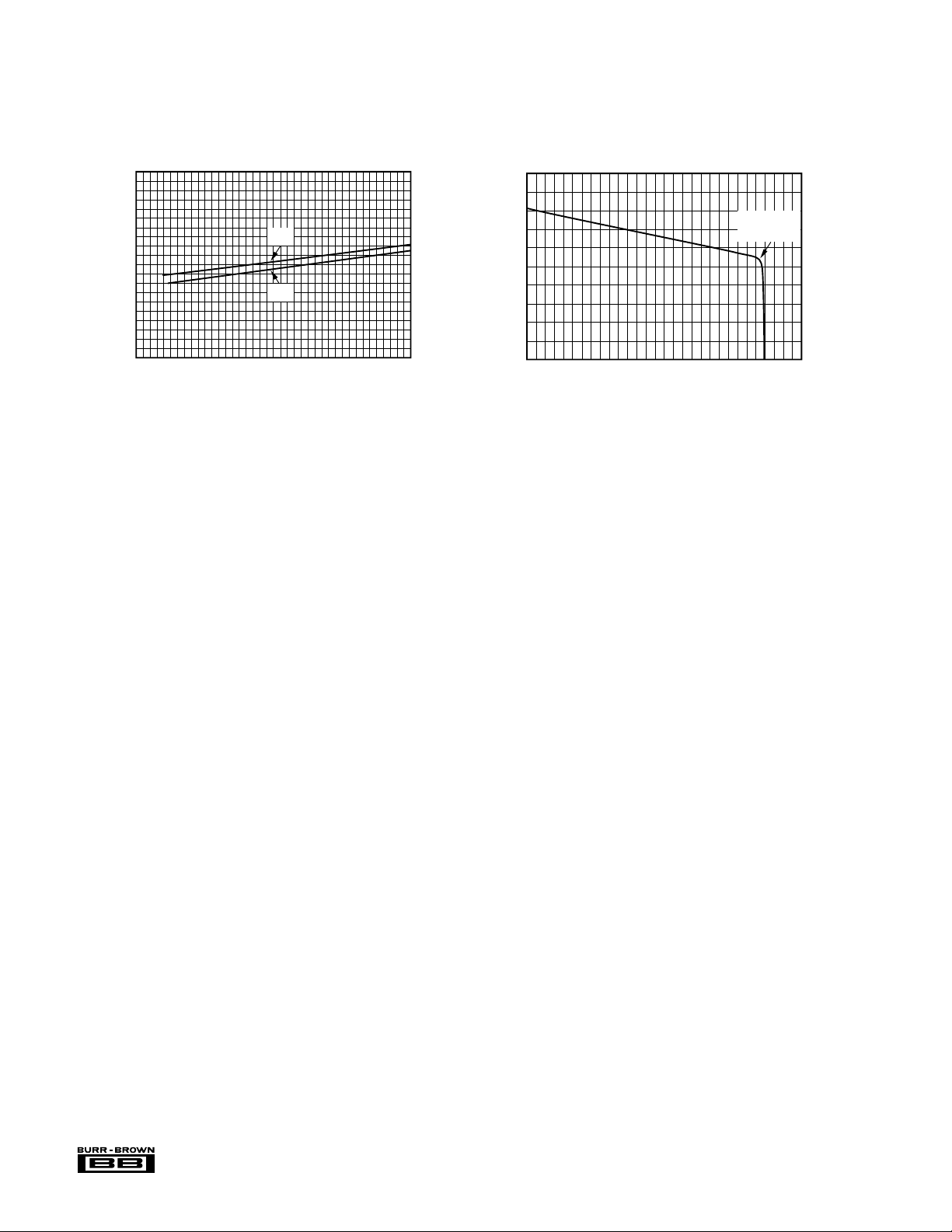
TYPICAL PERFORMANCE CURVES
At +25°C, ±VCC = 15VDC, and in circuit of Figure 1.
20
15
10
Supply Current (mA)
5
0
QUIESCENT CURRENT vs TEMPERATURE
+I
CC
–I
CC
25–75 –50 –25 0 50 75 100 125
Ambient Temperature (°C)
REFERENCE VOLTAGE vs REFERENCE LOAD CURRENT
5.01
5
4.99
VREF (V)
4.98
4.97
4.96
5 1015202530
0
Output Current (mA)
Short Circuit
Current Limit
THEORY OF OPERATION
The VFC100 monolithic voltage-to-frequency converter provides a digital pulse train output with an average frequency
proportional to the analog input voltage. The output is an
active low pulse of constant duration, with a repetition rate
determined by the input voltage. Falling edges of the output
pulses are synchronized with rising edges of the clock input.
Operation is similar to a conventional charge balance VFC.
An input operational amplifier (Figure 1) is configured as an
integrator so that a positive input voltage causes an input
current to flow in R
ramp negatively. When the output of the integrator crosses
the reference voltage (5V), the comparator trips, activating
the clocked logic circuit. Once activated, the clocked logic
awaits a falling edge of the clock input, followed by a rising
edge (see Figure 2). On the rising edge, switch S
®
. This forces the integrator output to
IN
VFC100
is closed
1
for one complete clock cycle, causing the reset current, I
switch to the integrator input. Since I
current, I
, the output of the integrator ramps positively
IN
is larger than the input
1
during the one clock cycle reset period. The clocked logic
circuitry also generates a VFC output pulse during the reset
period.
Unlike conventional VFC circuits, the VFC100 accurately
derives its reset period from an external clock frequency.
This eliminates the critical timing capacitor required by
other VFC circuits. One period (from rising edge to rising
edge) of the clock input determines the integrator reset
period.
When the negative-going integration of the input signal
crosses the comparator threshold, integration of the input
signal will continue until the reset period can start (awaiting
4
1
, to
C
+1V
–0.75V
10µ
1µ
0.1µ
0.01µ
1000p
100p
100 1k 10k 100k 1M
Full-Scale Frequency (Hz)
+2.5V
–1.9V
C
INT
(F)
* This is the maximum swing of the integrator output voltage
referred to the comparator noninverting input voltage.
Integrator Swing*
+100mV
–75mV
10M
INT
FCClock
TTL/CMOS
0.1µF
+V
+V
CC
0.1µF
L
54
I
IN
V
IN
R
7
6
20k
1mA
Integrator
IN
Ω
S
1
I
1
–V
CC
13
Analog
Ground
14
Comparator
15
FIGURE 1. Circuit Diagram for Voltage-to-Frequency Mode.
Clock
Integrator 5V
f
O
FIGURE 2. Timing Diagram for Voltage-to-Frequency Mode.
the necessary transitions of the clock). Output pulses are
thus made to align with rising edges of the external clock.
This causes the instantaneous output frequency to be a
subharmonic of the clock frequency. The average frequency,
however, will be an accurate analog of the input voltage.
A full scale input of 10V (or an input current of 0.5mA)
causes a nominal output frequency equal to half the clock
frequency. The transfer function is
= (VIN/20V) f
f
OUT
CLOCK
.
Figure 3 shows the transfer function graphically. Note that
inputs above 10V (or 0.5mA) do not cause an increase in the
output frequency. This is an easily detectable indication of
an overrange input. In the overrange condition, the integrator amplifier will ramp to its negative output swing limit.
10
Clocked
Logic
5V
Reference
16
1
+V
Output
One-Shot
9
+V
CC
–V
CC
11
12
CC
8
0.1µF
–V
CC
f
Digital
Ground
When the input signal returns to within the linear range, the
integrator amplifier will recover and begin ramping upward
during the reset period.
INSTALLATION AND
OPERATING INSTRUCTIONS
The integrator capacitor C
magnitude of the integrator voltage waveform. Its absolute
accuracy is not critical since it does not affect the transfer
function. This allows a wide range of capacitance to produce
excellent results. Figure 4 facilitates choosing an appropriate
(see Figure 1) affects the
INT
OUT
fFS= f
f
OUT
0
0
FIGURE 3 . T ransfer Function for Voltage-to-Frequency Mode.
CLOCK
/2
V
IN
IN
10V
0.5mAI
FIGURE 4. Integrator Capacitor Selection Graph.
®
5
VFC100
 Loading...