

Burr Brown VCA610UA-2K5, VCA610UA, VCA610U, VCA610PA, VCA610P Datasheet
©1992 Burr-Brown Corporation PDS-1140D Printed in U.S.A. January, 1995
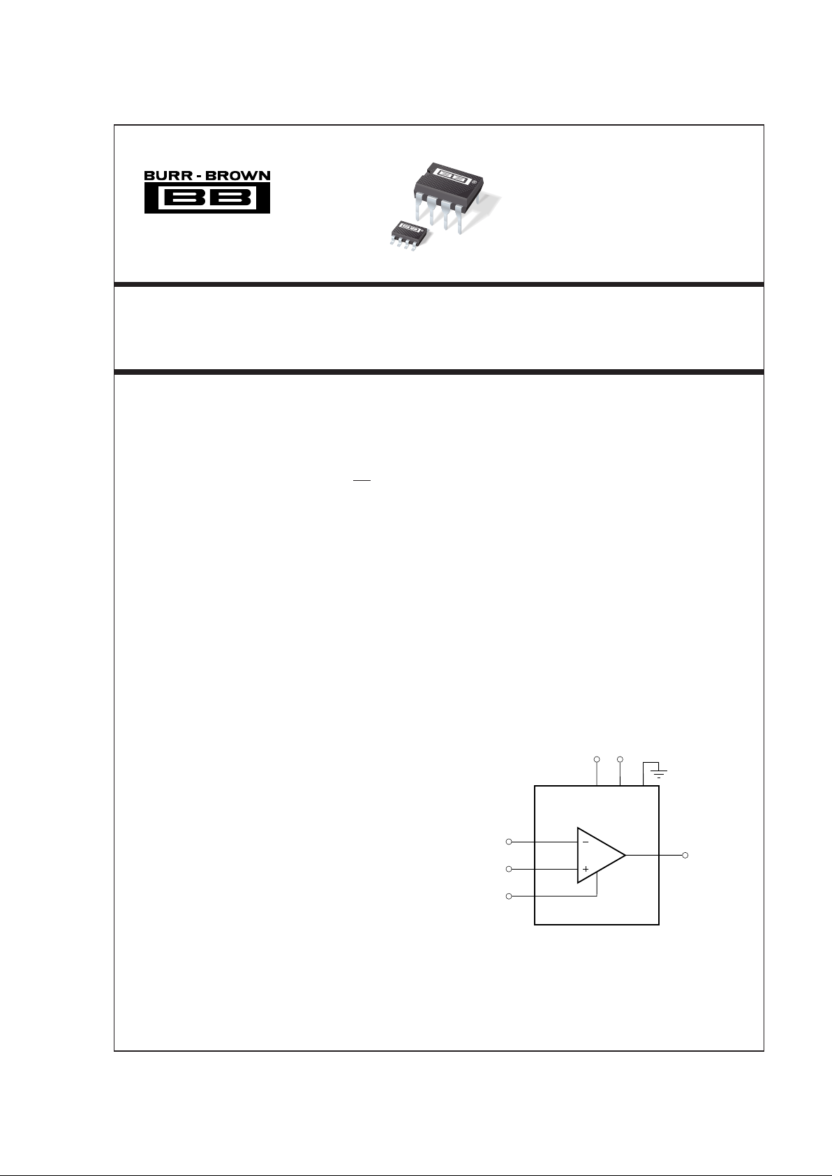
DESCRIPTION
The VCA610 is a wideband, continuously variable,
voltage controlled gain amplifier. It provides lineardB gain control with high impedance inputs. It is
designed to be used as a flexible gain control element
in a variety of electronic systems.
The VCA610 has a gain control range of 80dB (–40dB
to +40dB) providing both gain and attenuation for
maximum flexibility in a small 8-lead SO-8 or plastic
dual-in-line package. The broad attenuation range can
be used for gradual or controlled channel turn-on and
turn-off for applications in which abrupt gain changes
can create artifacts or other errors. In addition, the
output can be disabled to provide –80dB of attenuation. Group delay variation with gain is typically less
than ±2ns across a bandwidth of 1 to 15MHz.
The VCA610 has a noise figure of 3.5dB (with an R
S
of 200Ω) including the effects of both current and
voltage noise. Instantaneous output dynamic range is
70dB for gains of 0dB to +40dB with 1MHz noise
bandwidth. The output is capable of driving 100Ω.
The high speed, 300dB/µs, gain control signal is a
unipolar (0 to –2V) voltage that varies the gain linearly in dB/V.
VCA610
FEATURES
● WIDE GAIN CONTROL RANGE: 80dB
● SMALL PACKAGE: 8-pin SOIC or DIP
● WIDE BANDWIDTH: 30MHz
● LOW VOLTAGE NOISE: 2.2nV/
√Hz
● FAST GAIN SLEW RATE: 300dB/
µs
● EASY TO USE
WIDEBAND
VOLTAGE CONTROLLED AMPLIFIER
APPLICATIONS
● OPTICAL DISTANCE MEASUREMENT
● AGC AMPLIFIER
● ULTRASOUND
● SONAR
● ACTIVE FILTERS
● LOG AMPLIFIER
● IF CIRCUITS
● CCD CAMERAS
The VCA610 is designed with a very fast overload
recovery time of only 200ns. This allows a large
signal transient to overload the output at high gain,
without obscuring low-level signals following closely
behind. The excellent overload recovery time and
distortion specifications optimize this device for lowlevel doppler measurements.
+5V –5V
V
OUT
–In
+In
V
C
Gain
Control
VCA610
6
8
5
1
3
72
®
International Airport Industrial Park • Mailing Address: PO Box 11400, Tucson, AZ 85734 • Street Address: 6730 S. Tucson Blvd., Tucson, AZ 85706 • Tel: (520) 746-1111 • Twx: 910-952-1111
Internet: http://www.burr-brown.com/ • FAXLine: (800) 548-6133 (US/Canada Only) • Cable: BBRCORP • Telex: 066-6491 • FAX: (520) 889-1510 • Immediate Product Info: (800) 548-6132
VCA610
VCA610
®
VCA610
2
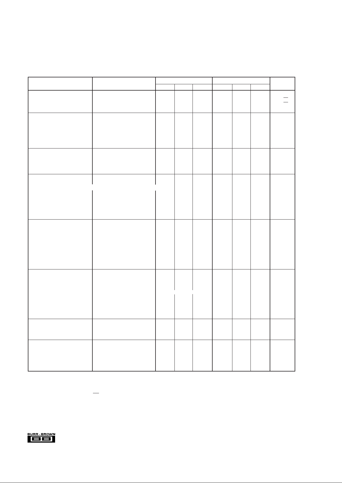
SPECIFICATIONS
ELECTRICAL
All specifications at VS = ±5V, RL = 500Ω, RS = 0Ω, and TA = +25°C, unless otherwise noted.
VCA610PA, UA VCA610P, U
PARAMETER CONDITIONS MIN TYP MAX MIN TYP MAX UNITS
NOTES: (1) See Input/Output Range discussion in Applications Information Section (Figure 2). (2) Gain is laser trimmed and tested at gains of –40dB, 0dB, +15dB,
+25dB, and +40dB; V
IN
=1Vp-p for gains less than 0dB; V
OUT
= 1V for gains of 0dB to +40dB. (3) Output offset change from offset at G = –40dB.
(4) Gain = +40dB; Input step of 2V to 2mV; time required for output to return from saturation to linear operation. (5) V
IN
= 7mVp-p, V
OUT
= 700mVp-p (250mVrms);
Output Power = –10dBm/tone, equal amplitude tones of 5MHz ±500Hz, G = +40dB. See typical performance curves. (6) With R
S
= 0Ω, and noise bandwidth of
1MHz. IDR = 20 log (V
ORMS
/(e
ORMS
x √BW)); where V
ORMS
is rms output voltage, e
ORMS
is output noise spectral density, and BW is noise bandwidth.
Symmetrical to Ground (±10%)
INPUT NOISE
Input Voltage Noise G = +40dB, R
S
= 0Ω 2.2 * nV/√Hz
Input Current Noise G = –40dB to +40dB 1.4 * pA/√Hz
Noise Figure G = +40dB, R
S
= 200Ω 3.5 * dB
INPUT
Input Impedance Common-Mode 1 || 1 * MΩ || pF
Bias Current All Gains 6 * µA
Offset Current All Gains 2 * µA
Differential Voltage Range
(1)
*
Common-Mode Voltage Range ±2.5 * V
Common-Mode Rejection 50 * dB
GAIN
Specified Gain Range –40 +40 * * dB
Gain Accuracy
(2)
–40dB ≤ G ≤ +40dB ±0.5 ±2 ±2 ±4dB
Gain Accuracy Temperature Drift T
A
= –25°C to +85°C ±0.01 * dB/°C
Gain with Output Disabled +0.1V ≤ V
C
≤ +2.0V, f = 1MHz –80 * dB
GAIN CONTROL
Gain Scaling Factor –40dB ≤ G ≤ +40dB 40 * dB/V
Control Voltage (V
C
) G = –40dB (VC = 0V) to +40dB (VC = –2V) 0 –2 * * V
Bandwidth –3dB 1 * MHz
Slew Rate 80dB Gain Step 300 * dB/µs
Settling Time: 1% V
IN
= 10mVDC, ∆ G = 80dB 800 * ns
Input Impedance 1 || 1 * MΩ || pF
Input Bias Current All Gains 2 * µA
Output Offset Change
(3)
∆ G = 80dB ±30 ±75 * ±125 mV
FREQUENCY RESPONSE
Bandwidth, Small-Signal –3dB, All Gains 30 * MHz
Bandwidth, Large-Signal V
O
= 1Vp-p, G ≥ 0dB 25 * MHz
Group Delay Unit-to-Unit Variation
0dB ≤ G ≤ +40dB f = 1 to 15MHz ±1*ns
–40dB ≤ G < 0dB f = 1 to 15MHz ±2*ns
Output Slew Rate V
O
= 1Vp-p 60 * V/µs
Overload Recovery
(4)
200 * ns
Two-tone Intermodulation Distortion
(5)
Small-Signal –50 * dBc
Two-tone, 3rd Order IMD Intercept
(5)
Small-Signal 15 * dBm
OUTPUT
Voltage Swing
(1)
G = +40dB ±1 ±1.6 * * V
G = 0dB ±0.5 ±0.75 * * V
Output Voltage Limit *
Short-Circuit Current Continuous to Common ±80 * mA
Instantaneous Dynamic Range (IDR)
(6)
G = 0dB to +40dB VO = 1.5Vp-p 70 * dB
Offset G = –40dB ±2 ±30 * * mV
Output Resistance f = 1MHz, All Gains 10 * Ω
POWER SUPPLY
Specification ±5V Recommended ±4.5 ±5.5 * * V
PSR G = 0dB 40 50 * dB
Quiescent Current –26/+30 ±32 * * mA
TEMPERATURE
Specification Applies to Temperature Drift Specs –25 +85 * * °C
Operation –40 +125 * * °C
Thermal Resistance,
θ
JA
P, PA 100 * °C/W
U, UA 125 * °C/W
®
VCA610
3
PIN CONFIGURATION
Top View DIP
SO-8
–V
S
7
+V
S
6
–In
8
V
OUT
5
VCA610
2
GND
31
+In
4
Gain
Control,
V
C
No
Internal
Connection
The information provided herein is believed to be reliable; however, BURR-BROWN assumes no responsibility for inaccuracies or omissions. BURR-BROWN assumes
no responsibility for the use of this information, and all use of such information shall be entirely at the user’s own risk. Prices and specifications are subject to change
without notice. No patent rights or licenses to any of the circuits described herein are implied or granted to any third party. BURR-BROWN does not authorize or warrant
any BURR-BROWN product for use in life support devices and/or systems.
ABSOLUTE MAXIMUM RATINGS
Supply .................................................................................................±7V
Differential Input Voltage...............................................................Total V
S
Input Voltage Range ..................................... See Input Protection Section
Storage Temperature Range .......................................... –65°C to +150°C
Lead Temperature (soldering, DIP, 10s)........................................+300°C
Lead Temperature (soldering, SO-8, 3s) ....................................... +260°C
Output Short-Circuit to Ground (+25°C)...................................Continuous
Junction Temperature (T
J
) ............................................................. +175°C
PACKAGE/ORDERING INFORMATION
PACKAGE DRAWING
PRODUCT PACKAGE NUMBER
(1)
VCA610PA 8-Pin Plastic DIP 006
VCA610P 8-Pin Plastic DIP 006
VCA610UA SO-8 Surface-Mount 182
VCA610U SO-8 Surface-Mount 182
NOTE:(1) For detailed drawing and dimension table, please see end of data
sheet, or Appendix C of Burr-Brown IC Data Book.
ELECTROSTATIC
DISCHARGE SENSITIVITY
This integrated circuit can be damaged by ESD. Burr-Brown
recommends that all integrated circuits be handled with
appropriate precautions. Failure to observe proper handling
and installation procedures can cause damage.
ESD damage can range from subtle performance degradation to complete device failure. Precision integrated circuits
may be more susceptible to damage because very small
parametric changes could cause the device not to meet its
published specifications.
®
VCA610
4
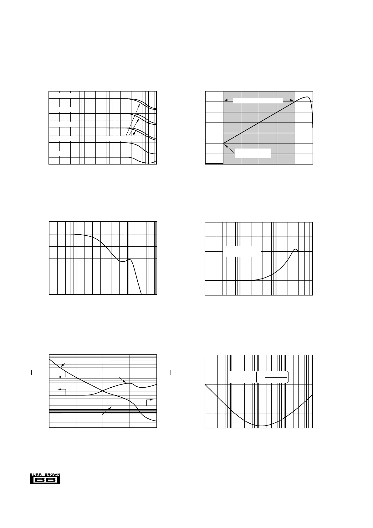
NOISE FIGURE vs SOURCE RESISTANCE
Source Resistance (Ω)
NF (dB)
25
20
15
10
5
0
10 100 1k 10k 100k
NFdB = 10 log 1 +
e
n
2
+ (inRS)
2
4kTR
S
VOLTAGE AND CURRENT NOISE
vs GAIN
Gain (dB)
10k
1k
100
10
1
–40 –20 0 +20 +40
Voltage Noise (nV/√Hz)
1k
100
10
1
0.1
Current Noise (pA/√Hz)
Output Voltage Noise
Input Current Noise
Input-Referred Voltage Noise
GAIN CONTROL RESPONSE
Frequency (Hz)
Normalized Response (dB)
3
0
–3
–6
–9
–12
–15
10k 100k 1M 10M 100M
GAIN vs CONTROL VOLTAGE
Control Voltage, V
C
(V)
Gain (dB)
60
40
20
0
–20
–40
–60
–80
0.5 0 –0.5 –1 –1.5 –2 –2.5
Output Disabled for
+0.1V ≤ V
C
≤ +2V
Specified Operating Range
SMALL-SIGNAL RESPONSE vs GAIN
Frequency (MHz)
0.1 1.0 10 100
Gain (dB)
50
40
30
20
10
0
–10
–20
–30
–40
–50
VC = –2.0V
VC = –1.5V
VC = –1.0V
VC = –0.5V
V
C
= 0V
Large Signal, VO = 1Vp-p
TYPICAL PERFORMANCE CURVES
At VS = ±5V, RL = 500Ω, RS = 0Ω, and TA = +25°C, unless otherwise noted.
FEEDTHRU WITH OUTPUT DISABLED
Frequency (MHz)
Disabled Gain (dB)
0
–20
–40
–60
–80
–100
0.1 1 10 100
Output Disabled for
+0.1V ≤ V
C
≤ +2V
 Loading...