

Burr Brown VCA2612Y-2K, VCA2612Y Datasheet
1
®
VCA2612
FEATURES
● LOW NOISE PREAMP:
• Low Input Noise: 1.25nV/√Hz
• Active Termination Noise Reduction
• Switchable Termination Value
• 80MHz Bandwidth
• 5dB to 25dB Gain
• Differential Input/Output
● LOW NOISE VARIABLE GAIN AMPLIFIER:
• Low Noise VCA: 3.3nV/√Hz, Differential
Programming Optimizes Noise Figure
• 24dB to 45dB Gain
• 40MHz Bandwidth
• Differential Input/Output
● LOW CROSSTALK:
52dB at Max Gain, 5MHz
● HIGH-SPEED VARIABLE GAIN ADJUST
● SWITCHABLE EXTERNAL PROCESSING
APPLICATIONS
● ULTRASOUND SYSTEMS
● WIRELESS RECEIVERS
● TEST EQUIPMENT
VCA2612
®
International Airport Industrial Park • Mailing Address: PO Box 11400, Tucson, AZ 85734 • Street Address: 6730 S. Tucson Blvd., Tucson, AZ 85706 • Tel: (520) 746-1111
Twx: 910-952-1111 • Internet: http://www.burr-brown.com/ • Cable: BBRCORP • Telex: 066-6491 • FAX: (520) 889-1510 • Immediate Product Info: (800) 548-6132
© 2000 Burr-Brown Corporation PDS-1541B Printed in U.S.A. March, 2000
TM
Dual, VARIABLE GAIN AMPLIFIER
with Low Noise Preamp
VCA2612
For most current data sheet and other product
information, visit www.burr-brown.com
Low Noise
Preamp
5dB to 25dB
Programmable
Gain Amplifier
24 to 45dB
Voltage
Controlled
Attenuator
Analog
Control
Maximum Gain
Select
RF
2
RF
1
FB
FBSW
LNP
IN
P
LNP
IN
N
LNP
GS1
LNP
GS2
LNP
GS3
LNP
Gain Set
Input
LNP
OUT
P
SEL
VCAINP
LNP
OUT
N VCAINN VCA
CNTL
FB
CNTL
VCA
OUT
P
VCA
OUT
N
MGS
1
MGS2MGS
3
Maximum Gain Select
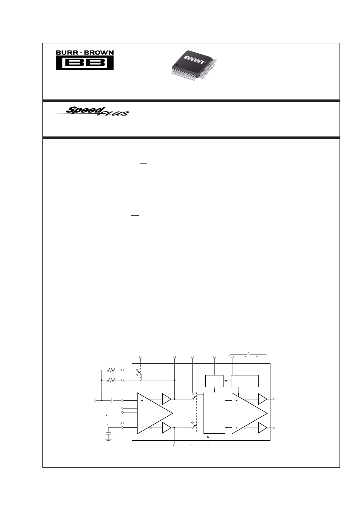
VCA2612
(1 of 2 Channels)
DESCRIPTION
The VCA2612 is a highly integrated, dual receive channel, signal processing subsystem. Each channel of the
product consists of a low noise pre-amplifier (LNP) and
a Variable Gain Amplifier (VGA). The LNP circuit
provides the necessary connections to implement Active
Termination (AT), a method of cable termination which
results in up to 4.6dB noise figure improvement. Different cable termination characteristics can be accommodated by utilizing the VCA2612’s switchable LNA feedback pins. The LNP has the ability to accept both
differential and single ended inputs, and generates a
differential output signal. The LNP provides strappable
gains of 5dB, 17dB, 22dB and 25dB.
The output of the LNP can be accessed externally for
further signal processing, or fed directly into the VGA.
The VCA2612’s VGA section consists of two parts, the
Voltage Controlled Attenuator (VCA) and the Programmable Gain Amplifier (PGA). The gain and gain range
of the Programmable Gain Amplifier can be digitally
programmed. The combination of these two programmable elements results in a variable gain ranging from
0dB up to a maximum gain as defined by the user
through external connections. The output of the VGA
can be used in either a single-ended or differential mode
to drive high performance analog-to-digital converters.
The VCA2612 also features low crosstalk and outstanding distortion performance. The combination of low
noise, and gain range programmability make the
VCA2612 a versatile building block in a number of
applications where noise performance is critical. The
VCA2612 is available in a TQFP-48 package.
2
®
VCA2612
The information provided herein is believed to be reliable; however, BURR-BROWN assumes no responsibility for inaccuracies or omissions. BURR-BROWN assumes
no responsibility for the use of this information, and all use of such information shall be entirely at the user’s own risk. Prices and specifications are subject to change
without notice. No patent rights or licenses to any of the circuits described herein are implied or granted to any third party. BURR-BROWN does not authorize or warrant
any BURR-BROWN product for use in life support devices and/or systems.
SPECIFICATIONS
At TA = +25°C, V
DD
= 5V, load resistance = 500Ω on each output to ground, MGS = 011, LNP = 22dB and fIN = 5MHz, unless otherwise noted. The input to the
preamp (LNP) is single-ended, and the output from the VCA is single-ended unless otherwise noted.
VCA2612Y
PARAMETER CONDITIONS MIN TYP MAX UNITS
PREAMPLIFIER
Input Resistance 600 kΩ
Input Capacitance 15 pF
Input Bias Current 1nA
CMRR f = 1MHz, VCA
CNTL
= 0.2V 50 dB
Maximum Input Voltage Preamp Gain = +5dB 1 Vp-p
Preamp Gain = +25dB 112 mVp-p
Input Voltage Noise
(1)
Preamp Gain = +5dB 3.5 nV/√Hz
Preamp Gain = +25dB 1.25 nV/√Hz
Input Current Noise Independent of Gain 350 fA/√Hz
Noise Figure, R
S
= 75Ω, RIN = 75Ω
(1)
RF = 550Ω, PreAmp Gain = 22dB, 6.2 dB
PGA Gain = 39dB
Bandwidth Gain = 22dB 80 MHz
PROGRAMMABLE VARIABLE GAIN AMPLIFIER
Peak Input Voltage Differential 2 Vp-p
–3dB Bandwidth 40 MHz
Slew Rate 300 V/µs
Output Signal Range R
L
≥ 500Ω Each Side to Ground 2.5 ±1V
Output Impedance f = 5MHz 1 Ω
Output Short-Circuit Current ±40 mA
Third Harmonic Distortion f = 5MHz, V
OUT
= 1Vp-p, VCA
CNTL
= 3.0V –45 –71 dBc
Second Harmonic Distortion f = 5MHz, V
OUT
= 1Vp-p, VCA
CNTL
= 3.0V –45 –63 dBc
IMD, Two-Tone V
OUT
= 2Vp-p, f = 1MHz –80 dBc
V
OUT
= 2Vp-p, f = 10MHz –80 dBc
1dB Compression Point f = 5MHz, Output Referred, Differential 6 Vp-p
Crosstalk
V
OUT
= 1Vp-p, f = 1MHz, Max Gain Both Channels
68 dB
Group Delay Variation 1MHz < f < 10MHz, Full Gain Range ±2ns
ACCURACY
Gain Slope 10.9 dB/V
Gain Error ±1
(2)
dB
Output Offset Voltage ±50 mV
GAIN CONTROL INTERFACE
Input Voltage (VCA
CNTL
) Range 0 to 3.0 V
Input Resistance 1MΩ
Response Time 45dB Gain Change, MGS = 111 0.2 µs
POWER SUPPLY
Specified Operating Range 4.75 5.0 5.25 V
Power Dissipation Operating, Both Channels 410 475 mW
NOTE: (1) For preamp driving VGA. (2) Referenced to best fit dB-linear curve.

3
®
VCA2612
ELECTROSTATIC
DISCHARGE SENSITIVITY
This integrated circuit can be damaged by ESD. Burr-Brown
recommends that all integrated circuits be handled with
appropriate precautions. Failure to observe proper handling
and installation procedures can cause damage.
ESD damage can range from subtle performance degradation to complete device failure. Precision integrated circuits
may be more susceptible to damage because very small
parametric changes could cause the device not to meet its
published specifications.
ABSOLUTE MAXIMUM RATINGS
Power Supply (+VS) ............................................................................. +6V
Analog Input ............................................................. –0.3V to (+V
S
+ 0.3V)
Logic Input ............................................................... –0.3V to (+V
S
+ 0.3V)
Case Temperature ......................................................................... +100°C
Junction Temperature .................................................................... +150°C
Storage Temperature...................................................... –40°C to +150°C
PACKAGE SPECIFIED
DRAWING TEMPERATURE PACKAGE ORDERING TRANSPORT
PRODUCT PACKAGE NUMBER RANGE MARKING NUMBER
(1)
MEDIA
VCA2612Y TQFP-48 Surface Mount 355 –40°C to +85°C A12 VCA2612Y/250 Tape and Reel
"""""VCA2612Y/2K "
NOTE: (1) Models with a slash (/) are available only in Tape and Reel in the quantities indicated (e.g., /2K indicates 2000 devices per reel). Ordering 2000 pieces
of “VCA2612Y/2K” will get a single 2000-piece Tape and Reel.
PACKAGE/ORDERING INFORMATION
4
®
VCA2612
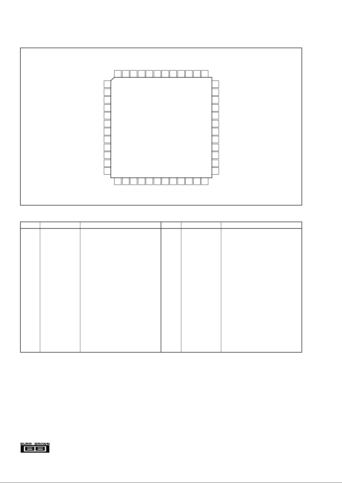
PIN CONFIGURATION
1V
DD
A Channel A +Supply
2 NC Do Not Connect
3 NC Do Not Connect
4 VCA
IN
NA Channel A VCA Negative Input
5 VCA
IN
PA Channel A VCA Positive Input
6 LNP
OUT
NA Channel A LNP Negative Output
7 LNP
OUT
PA Channel A LNP Positive Output
8 SWFBA Channel A Switched Feedback Output
9 FBA Channel A Feedback Output
10 COMP1A Channel A Frequency Compensation 1
11 COMP2A Channel A Frequency Compensation 2
12 LNP
IN
NA Channel A LNP Inverting Input
13 LNP
GS3
A Channel A LNP Gain Strap 3
14 LNP
GS2
A Channel A LNP Gain Strap 2
15 LNP
GS1
A Channel A LNP Gain Strap 1
16 LNP
IN
PA Channel A LNP Noninverting Input
17 V
DD
R +Supply for Internal Reference
18 V
BIAS
0.01µF Bypass to Ground
19 V
CM
0.01µF Bypass to Ground
20 GNDR Ground for Internal Reference
21 LNP
IN
PB Channel B LNP Noninverting Input
22 LNP
GS1
B Channel B LNP Gain Strap 1
23 LNP
GS2
B Channel B LNP Gain Strap 2
24 LNP
GS3
B Channel B LNP Gain Strap 3
25 LNP
IN
NB Channel B LNP Inverting Input
26 COMP2B Channel B Frequency Compensation 2
27 COMP1B Channel B Frequency Compensation 1
28 FBB Channel B Feedback Output
29 SWFBB Channel B Switched Feedback Output
30 LNP
OUT
PB Channel B LNP Positive Output
31 LNP
OUT
NB Channel B LNP Negative Output
32 VCA
IN
PB Channel B VCA Positive Input
33 VCA
IN
NB Channel B VCA Negative Input
34 NC Do Not Connect
35 NC Do Not Connect
36 V
DD
B Channel B +Analog Supply
37 GNDB Channel B Analog Ground
38 VCA
OUT
NB Channel B VCA Negative Output
39 VCA
OUT
PB Channel B VCA Positive Output
40 MGS
3
Maximum Gain Select 3 (LSB)
41 MGS
2
Maximum Gain Select 2
42 MGS
1
Maximum Gain Select 1 (MSB)
43 VCA
CNTL
VCA Control Voltage
44 VCA
IN
SEL VCA Input Select, HI = External
45 FBSW
CNTL
Feedback Switch Control: HI = ON,
46 VCA
OUT
PA Channel A VCA Positive Output
47 VCA
OUT
NA Channel A VCA Negative Output
48 GNDA Channel A Analog Ground
PIN
DESIGNATOR
DESCRIPTION PIN
DESIGNATOR
DESCRIPTION
PIN DESCRIPTIONS
36
35
34
33
32
31
30
29
28
27
26
25
VDDB
NC
NC
VCA
IN
NB
VCA
IN
PB
LNP
OUT
NB
LNP
OUT
PB
SWFBB
FBB
COMP1B
COMP2B
LNP
IN
NB
GNDA
VCA
OUT
NA
VCA
OUT
PA
FBSW
CNTL
VCA
IN
SEL
VCA
CNTL
MGS1MGS2MGS3VCA
OUT
PB
VCA
OUT
NB
GNDB
LNP
GS3
A
LNP
GS2
A
LNP
GS1
A
LNP
IN
PA
V
DD
R
V
BIAS
V
CM
GNDR
LNP
IN
PB
LNP
GS1
B
LNP
GS2
B
LNP
GS3
B
1
2
3
4
5
6
7
8
9
10
11
12
VDDA
NC
NC
VCA
IN
NA
VCA
IN
PA
LNP
OUT
NA
LNP
OUT
PA
SWFBA
FBA
COMP1A
COMP2A
LNP
IN
NA
48 47 46 45 44 43 42
41 40 39 38
13 14 15 16 17 18 19 20 21 22 233724
VCA2612
5
®
VCA2612
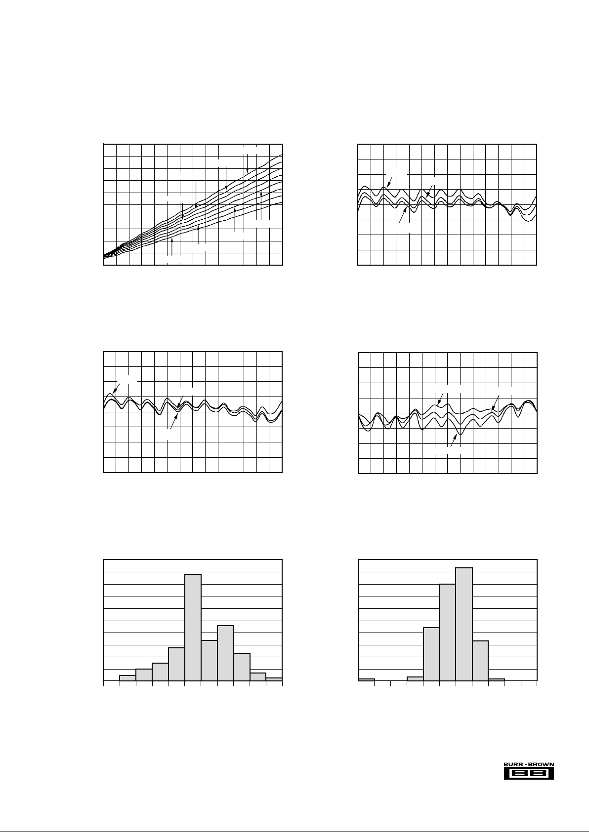
TYPICAL PERFORMANCE CURVES
At TA = +25°C, V
DD
= 5V, load resistance = 500Ω on each output to ground, MGS = 011, LNP = 22dB and fIN = 5MHz, unless otherwise noted. The input to the
preamp (LNP) is single-ended, and the output from the VCA is single-ended unless otherwise noted.
GAIN vs VCA
CNTL
VCA
CNTL
(V)
0.2 1.21.00.4 0.6 0.8 1.8 2.0 2.21.61.4 2.4 2.6 2.8 3.0
Gain (dB)
65
60
55
50
45
40
35
30
25
20
15
MGS = 111
MGS = 110
MGS = 101
MGS = 100
MGS = 011
MGS = 010
MGS = 001
MGS = 000
GAIN ERROR vs TEMPERATURE
VCA
CNTL
(V)
0.2 1.0 1.20.80.4 0.6 2.0 2.21.4 1.6 1.8 2.4 2.6 2.8 3.0
Gain Error (dB)
2.0
1.5
1.0
0.5
0
–0.5
–1.0
–1.5
–2.0
+25°C
–40°C
+85°C
GAIN ERROR vs VCA
CNTL
VCA
CNTL
(V)
0.2 1.0 1.20.80.4 0.6 2.0 2.21.4 1.6 1.8 2.4 2.6 2.8 3.0
Gain Error (dB)
2.0
1.5
1.0
0.5
0
–0.5
–1.0
–1.5
–2.0
10MHz
1MHz
5MHz
GAIN ERROR vs VCA
CNTL
VCA
CNTL
(V)
0.2 1.0 1.20.80.4 0.6 2.0 2.21.4 1.6 1.8 2.4 2.6 2.8 3.0
Gain Error (dB)
2.0
1.5
1.0
0.5
0
–0.5
–1.0
–1.5
–2.0
MGS = 011
MGS = 000
MGS = 111
GAIN MATCH: CHA to CHB = 0.2V
Delta Gain (dB)
–0.5 –0.4 –0.3 –0.2 –0.1 0.0 0.1 0.2 0.3 0.4 0.5
Units
100
90
80
70
60
50
40
30
20
10
0
GAIN MATCH: CHA to CHB = 3.0V
Delta Gain (dB)
–0.5 –0.4 –0.3 –0.2 –0.1 0.0 0.1 0.2 0.3 0.4 0.5
Units
100
90
80
70
60
50
40
30
20
10
0
6
®
VCA2612
TYPICAL PERFORMANCE CURVES (Cont.)
At TA = +25°C, V
DD
= 5V, load resistance = 500Ω on each output to ground, MGS = 011, LNP = 22dB and fIN = 5MHz, unless otherwise noted. The input to the
preamp (LNP) is single-ended, and the output from the VCA is single-ended unless otherwise noted.
GAIN vs FREQUENCY
(Pre-Amp)
Frequency (MHz)
0.1 1 10 100
Gain (dB)
30
25
20
15
10
5
0
LNP = 25dB
LNP = 22dB
LNP = 17dB
LNP = 5dB
GAIN vs FREQUENCY
(VCA and PGA, VCA
CNTL
= 0.2V)
Frequency (MHz)
0.1 1 10 100
Gain (dB)
5.0
4.0
3.0
2.0
1.0
0.0
–1.0
–2.0
–3.0
–4.0
–5.0
MGS = 111
MGS = 100
MGS = 011
MGS = 000
GAIN vs FREQUENCY
(VCA and PGA, VCA
CNTL
= 3.0V)
Frequency (MHz)
0.1 1 10 100
Gain (dB)
45
40
35
30
25
20
15
10
5
0
MGS = 111
MGS = 100
MGS = 011
MGS = 000
GAIN vs FREQUENCY
(VCA
CNTL
= 3.0V)
Frequency (MHz)
0.1 1 10 100
Gain (dB)
60
50
40
30
20
10
0
LNP = 25dB
LNP = 22dB
LNP = 5dB
LNP = 17dB
GAIN vs FREQUENCY
(LNP = 22dB)
Frequency (MHz)
0.1 1 10 100
Gain (dB)
60
50
40
30
20
10
0
VCA
CNTL
= 3.0V
VCA
CNTL
= 1.6V
VCA
CNTL
= 0.2V
OUTPUT REFERRED NOISE vs VCA
CNTL
VCA
CNTL
(V)
0 1.0 1.20.4 0.6 0.8 1.8 2.01.4 1.6 2.2 2.4 2.6 2.8 3.0
Noise (nv/√Hz)
1800
1600
1400
1200
1000
800
600
400
200
0
RS= 50Ω
MGS = 111
MGS = 011
 Loading...