

Page 1
UNIVERSAL ACTIVE FIL TER
UAF42
UAF42
UAF42
FEATURES
● VERSATILE—
LOW-PASS, HIGH-PASS
BAND-PASS, BAND-REJECT
● SIMPLE DESIGN PROCEDURE
● ACCURATE FREQUENCY AND Q —
INCLUDES ON CHIP 1000pF
±0.5%
CAPACITORS
DESCRIPTION
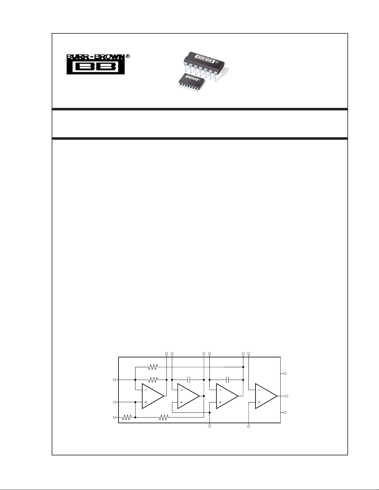
The UAF42 is a universal active filter which can be
configured for a wide range of low-pass, high-pass,
and band-pass filters. It uses a classical state-variable
analog architecture with an inverting amplifier and
two integrators. The integrators include on-chip 1000pF
capacitors trimmed to 0.5%. This solves one of the
most difficult problems of active filter design—
obtaining tight tolerance, low-loss capacitors.
A DOS-compatible filter design program allows easy
implementation of many filter types such as
Butterworth, Bessel, and Chebyshev. A fourth, uncommitted FET-input op amp (identical to the other
APPLICATIONS
● TEST EQUIPMENT
● COMMUNICATIONS EQUIPMENT
● MEDICAL INSTRUMENTATION
● DATA ACQUISITION SYSTEMS
● MONOLITHIC REPLACEMENT FOR UAF41
three) can be used to form additional stages, or for
special filters such as band-reject and Inverse
Chebyshev.
The classical topology of the UAF42 forms a timecontinuous filter, free from the anomalies and switching noise associated with switched-capacitor filter
types.
The UAF42 is available in 14-pin plastic DIP and
SOL-16 surface-mount packages, specified for the –
25°C to +85°C temperature range.
SBFS002
High-Pass
Out
R
R
In
1
In
2
R
In
3
R = 50kΩ ±0.5%
International Airport Industrial Park • Mailing Address: PO Box 11400, Tucson, AZ 85734 • Street Address: 6730 S. Tucson Blvd., Tucson, AZ 85706 • Tel: (520) 746-1111 • Twx: 910-952-1111
Internet: http://www.burr-brown.com/ • FAXLine: (800) 548-6133 (US/Canada Only) • Cable: BBRCORP • Telex: 066-6491 • FAX: (520) 889-1510 • Immediate Product Info: (800) 548-6132
©
1990 Burr-Brown Corporation PDS-1070H Printed in U.S.A. January, 1998
Band-Pass
1000pF
R
NOTE: (1) ±0.5%
Out
(1)
GND
Low-Pass
1000pF
Out
(1)
V+
V–
Page 2
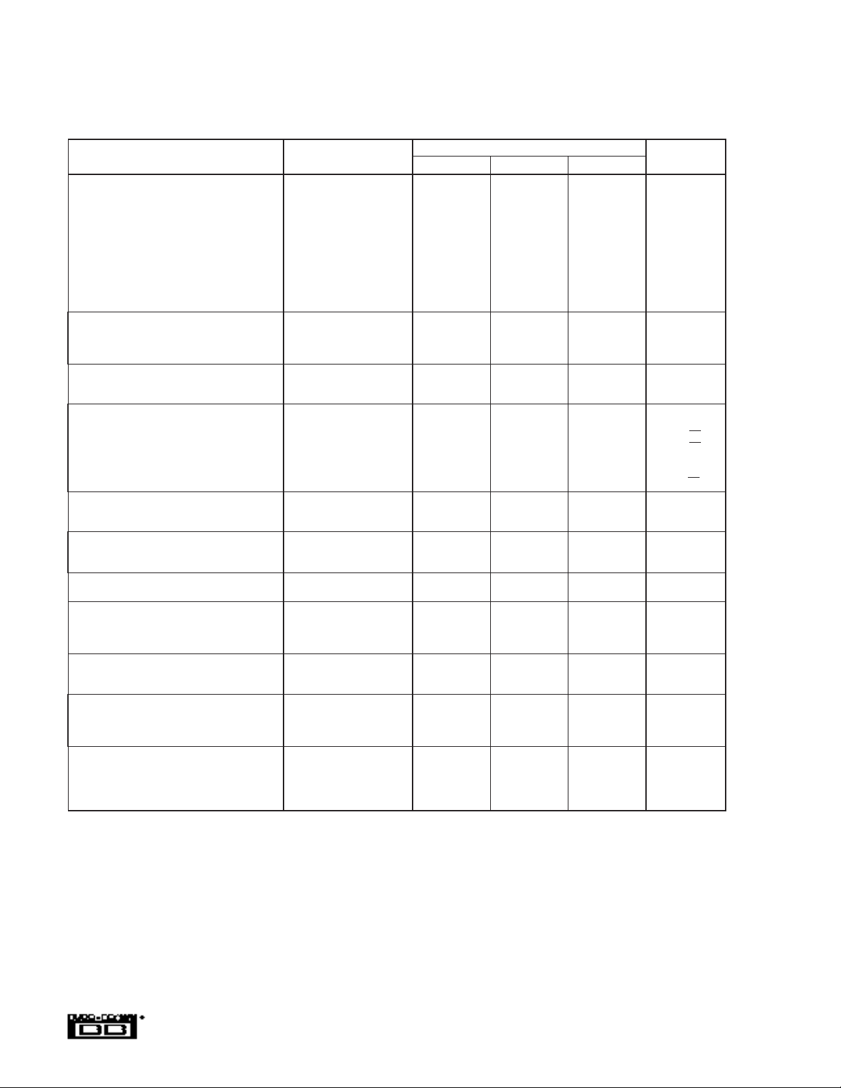
SPECIFICATIONS
ELECTRICAL
At TA = +25°C, VS = ±15V, unless otherwise noted.
UAF42AP, AU
PARAMETER CONDITIONS MIN TYP MAX UNITS
FILTER PERFORMANCE
Frequency Range, fn 0 to 100 kHz
Frequency Accuracy f = 1kHz 1 %
vs Temperature 0.01 %/°C
Maximum Q 400 —
Maximun (Q • Frequency) Product 500 kHz
Q vs Temperature (f
Q Repeatability (f
Offset Voltage, Low-Pass Output ±5mV
O
(f
O
O
Resistor Accuracy 0.5 1% %
OFFSET VOLTAGE
(1)
Input Offset Voltage ±0.5 ±5mV
vs Temperature ±3 µV/°C
vs Power Supply V
INPUT BIAS CURRENT
(1)
= ±6 to ±18V 80 96 dB
S
Input Bias Current VCM = 0V 10 50 pA
Input Offset Current V
NOISE
Input Voltage Noise
Noise Density: f = 10Hz 25 nV/√Hz
f = 10kHz 10 nV/√Hz
Voltage Noise: BW = 0.1 to 10Hz 2 µVp-p
Input Bias Current Noise
Noise Density: f = 10kHz 2 fA/√Hz
INPUT VOLTAGE RANGE
(1)
Common-Mode Input Range ±11.5 V
Common-Mode Rejection V
INPUT IMPEDANCE
(1)
Differential 1013 || 2 Ω || pF
Common-Mode 10
OPEN-LOOP GAIN
(1)
Open-Loop Voltage Gain VO = ±10V, RL = 2kΩ 90 126 dB
FREQUENCY RESPONSE
(1)
Slew Rate 10 V/µs
Gain-Bandwidth Product G = +1 4 MHz
Total Harmonic Distortion G = +1, f = 1kHz 0.0004 %
(1)
OUTPUT
Voltage Output RL = 2kΩ±11 ±11.5 V
Short Circuit Current ±25 mA
POWER SUPPLY
Specified Operating Voltage ±15 V
Operating Voltage Range ±6 ±18 V
Current ±6 ±7mA
TEMPERATURE RANGE
Specification –25 +85 °C
Operating –25 +85 °C
Storage –40 +125 °C
Thermal Resistance,
θ
JA
✻ Same as specification for UAF42AP.
NOTES: (1) Specifications apply to uncommitted op amp, A
. The three op amps forming the filter are identical to A4 but are tested as a complete filter.
4
4
• Q) < 10
5
• Q) < 10
5
• Q) < 10
= 0V 5 pA
CM
= ±10V 80 96 dB
CM
0.01 %/°C
0.025 %/°C
2%
13
|| 6 Ω || pF
100 °C/W
The information provided herein is believed to be reliable; however, BURR-BROWN assumes no responsibility for inaccuracies or omissions. BURR-BROWN assumes
no responsibility for the use of this information, and all use of such information shall be entirely at the user’s own risk. Prices and specifications are subject to change
without notice. No patent rights or licenses to any of the circuits described herein are implied or granted to any third party. BURR-BROWN does not authorize or warrant
any BURR-BROWN product for use in life support devices and/or systems.
UAF42
2
Page 3

PIN CONFIGURATION
Top View
Low-Pass V
V
V
Auxiliary Op Amp, +In
Auxiliary Op Amp, –In
Auxiliary Op Amp, V
Bandpass V
O
IN3
IN2
O
O
Plastic DIP, P
1
2
3
4
5
6
7
14
Frequency Adj
13
High-Pass V
12
V
IN1
11
Ground
10
V+
9
V–
8
Frequency Adj
2
O
1
ABSOLUTE MAXIMUM RATINGS
Power Supply Voltage ....................................................................... ±18V
Input Voltage............................................................................. ±V
Output Short Circuit .................................................................Continuous
Operating Temperature:
Plastic DIP, P; SOIC, U ................................................. –40°C to +85°C
Storage Temperature:
Plastic DIP, P; SOIC, U ............................................... –40°C to +125°C
Junction Temperature:
Plastic DIP, P; SOIC, U .............................................................. +125°C
Lead Temperature (soldering, 10s)................................................ +300°C
S
±0.7V
U Package
SOL-16, 16-Pin SOIC
Low-Pass V
NC
V
V
Auxiliary Op Amp, +In
Auxiliary Op Amp, –In
Auxiliary Op Amp, V
Bandpass V
NOTE: NC: No Connection. For best
performance connect all “NC” pins to
ground to minimize inter-lead capacitance.
1
O
2
3
IN3
4
IN2
5
6
7
O
8
O
16
Frequency Adj
15
NC
14
High-Pass V
13
V
IN1
12
Ground
11
V+
10
V–
9
Frequency Adj
2
O
1
PACKAGE/ORDERING INFORMATION
PACKAGE
DRAWING TEMPERATURE
PRODUCT PACKAGE NUMBER
UAF42AP Plastic 14-pin DIP 010 –25°C to +85°C
UAF42AU SOL-16 211 –25°C to +85°C
NOTE: (1) For detailed drawing and dimension table, please see end of data
sheet, or Appendix C of Burr-Brown IC Data Book.
(1)
RANGE
ELECTROSTATIC
DISCHARGE SENSITIVITY
This integrated circuit can be damaged by ESD. Burr-Brown
recommends that all integrated circuits be handled with
appropriate precautions. Failure to observe proper handling
and installation procedures can cause damage.
ESD damage can range from subtle performance degradation
to complete device failure. Precision integrated circuits may
be more susceptible to damage because very small parametric
changes could cause the device not to meet its published
specifications.
3
UAF42
Page 4

APPLICATIONS INFORMATION
The UAF42 is a monolithic implementation of the proven
state-variable analog filter topology. Pin-compatible with
the popular UAF41 Analog Filter, it provides several
improvements.
Slew Rate of the UAF42 has been increased to 10V/µs
versus 1.6V/µs for the UAF41. Frequency • Q product of
the UAF42 has been improved, and the useful natural
frequency extended by a factor of four to 100kHz. FETinput op amps on the UAF42 provide very low input bias
current. The monolithic construction of the UAF42 provides
lower cost and improved reliability.
DESIGN PROGRAM
Application Bulletin AB-035 and a computer-aided design
program, available from Burr-Brown, make it easy to design
and implement many kinds of active filters. The DOScompatible program guides you through the design process
and automatically calculates component values.
Low-pass, high-pass, band-pass and band-reject (notch)
filters can be designed. The program supports the three most
commonly used all-pole filter types: Butterworth, Chebyshev
and Bessel. The less-familiar Inverse Chebyshev is also
supported, providing a smooth passband response with ripple
in the stop-band.
With each data entry, the program automatically calculates
and displays filter performance. This allows a spreadsheetlike “what if” design approach. For example, you can quickly
determine, by trial and error, how many poles are required
for a desired attenuation in the stopband. Gain/phase plots
may be viewed for any response type.
The basic building element of the most commonly used filter
types is the second-order section. This section provides a
complex-conjugate pair of poles. The natural frequency, ω
and Q of the pole pair determines the characteristic response
of the section. The low-pass transfer function is
2
VO(s)
VI(s)
ALPω
=
2
+ s ωn/Q + ω
s
n
2
n
(1)
The high-pass transfer function is
2
VHP(s)
VI(s)
=
AHPs
2
+ s ωn/Q + ω
s
2
n
(2)
The band-pass transfer function is
V
(s)
BP
VI(s)
ABP(ωn/Q) s
=
2
s
+ s ωn/Q + ω
2
n
(3)
A band-reject response is obtained by summing the low-pass
and high-pass outputs, yielding the transfer function
V
BR
VI(s)
(s)
=
ABR(s2 +ω
2
+ s ωn/Q + ω
s
2
)
n
2
n
(4)
The most commonly used filter types are formed with one or
more cascaded second-order sections. Each section is designed for ω
and Q according to the filter type (Butterworth,
n
Bessel, Chebyshev, etc.) and cutoff frequency. While tabulated data can be found in virtually any filter design text, the
design program eliminates this tedious procedure.
Second-order sections may be non-inverting (Figure 1) or
inverting (Figure 2). Design equations for these two basic
configurations are shown for reference. The design program
solves these equations, providing complete results, including component values.
,
n
UAF42
4
Page 5

LP OutBP OutHP Out
R
F1
13 8 7 14
R
1
50kΩ
R
2
2
50kΩ
C
1
1000pF
R
F2
112
C
2
1000pF
50kΩ
R
V
G
IN
3
R
Q
A
1
R
4
50kΩ
A
2
A
3
UAF42
11
NOTE: If R
gain-setting resistor by connecting V
= 50kΩ, you can eliminate the external
G
to pin 2. Pin numbers are for DIP
IN
package. SOL-16 pinout
is different.
Design Equations
R
1
1 +
R
=
R
G
R
=
R
R
=
R
2
1
1
1
+
+
R
R
2
A
1
4
G
R
G
Q
4
R
2
1 +
R
=
LP
R
G
1
1
1
1
+
+
R
R
R
G
Q
4
1. ω
2. Q =
3. QA
n2
=
LP
R1 R
R4 (RG + RQ)
1 +
1 +
= QA
R
2
F1 RF2 C1 C2
R
G RQ
R
2
R
1
R
1
HP
R
2
= A
4. A
LP
F1 C1
F2 C2
F1 C1
F2 C2
1/2
5. A
HP
1/2
6. A
BP
R2 R
R1 R
R1 R
BP
R2 R
FIGURE 1. Non-Inverting Pole-Pair.
5
UAF42
Page 6

LP OutBP OutHP Out
R
V
IN
G
R
F1
13 8 7 14
R
1
50kΩ
R
2
2
50kΩ
C
1
1000pF
R
F2
112
C
2
1000pF
50kΩ
A
3
R
Q
1
R
4
50kΩ
A
2
A
3
UAF42
11
NOTE: If R
Q-setting resistor by connecting pin 2 to ground.
= 50kΩ, you can eliminate the external
Q
Pin numbers are for DIP
package. SOL-16 pinout
is different.
Design Equations
1. ω
n2
=
R1 R
F1 RF2 C1 C2
R
2
4. A
R
1
=
LP
R
G
2. Q =
3. QA
1 +
= QA
LP
FIGURE 2. Inverting Pole-Pair.
R
4
R
Q
HP
1
1
1
+
+
R
R
1
2
R
1
= A
BP
R
2
1
R
G
R1 R
R2 R
R
R1 R2 R
F1 C1
F2 C2
F1 C1
1/2
F2 C2
1/2
5. A
6. A
BP
R
=
HP
R
=
1 +
R
2
1
2
A
=
LP
R
G
R
4
R
Q
1
1
1
1
+
R
G
+
R
R
R
1
2
G
UAF42
6
Page 7

PACKAGE OPTION ADDENDUM
www.ti.com
28-Nov-2005
PACKAGING INFORMATION
Orderable Device Status
(1)
Package
Type
Package
Drawing
Pins Package
Qty
Eco Plan
UAF42AP ACTIVE PDIP N 14 25 TBD Call TI Level-NA-NA-NA
UAF42AP-1 OBSOLETE PDIP N 14 TBD Call TI Call TI
UAF42AU ACTIVE SOIC DW 16 48 Pb-Free
UAF42AU-1 OBSOLETE SOIC DW 16 TBD Call TI Call TI
UAF42AUE4 ACTIVE SOIC DW 16 48 Pb-Free
(1)
The marketing status values are defined as follows:
ACTIVE: Product device recommended for new designs.
LIFEBUY: TI has announced that the device will be discontinued, and a lifetime-buy period is in effect.
NRND: Not recommended for new designs. Device is in production to support existing customers, but TI does not recommend using this part in
a new design.
PREVIEW: Device has been announced but is not in production. Samples may or may not be available.
OBSOLETE: TI has discontinued the production of the device.
(2)
Eco Plan - The planned eco-friendly classification: Pb-Free (RoHS) or Green (RoHS & no Sb/Br) - please check
http://www.ti.com/productcontent for the latest availability information and additional product content details.
TBD: The Pb-Free/Green conversion plan has not been defined.
Pb-Free (RoHS): TI's terms "Lead-Free" or "Pb-Free" mean semiconductor products that are compatible with the current RoHS requirements
for all 6 substances, including the requirement that lead not exceed 0.1% by weight in homogeneous materials. Where designed to be soldered
at high temperatures, TI Pb-Free products are suitable for use in specified lead-free processes.
Green (RoHS & no Sb/Br): TI defines "Green" to mean Pb-Free (RoHS compatible), and free of Bromine (Br) and Antimony (Sb) based flame
retardants (Br or Sb do not exceed 0.1% by weight in homogeneous material)
(RoHS)
(RoHS)
(2)
Lead/Ball Finish MSL Peak Temp
CU NIPDAU Level-3-260C-168 HR
CU NIPDAU Level-3-260C-168 HR
(3)
(3)
MSL, Peak Temp. -- The Moisture Sensitivity Level rating according to the JEDEC industry standard classifications, and peak solder
temperature.
Important Information and Disclaimer:The information provided on this page represents TI's knowledge and belief as of the date that it is
provided. TI bases its knowledge and belief on information provided by third parties, and makes no representation or warranty as to the
accuracy of such information. Efforts are underway to better integrate information from third parties. TI has taken and continues to take
reasonable steps to provide representative and accurate information but may not have conducted destructive testing or chemical analysis on
incoming materials and chemicals. TI and TI suppliers consider certain information to be proprietary, and thus CAS numbers and other limited
information may not be available for release.
In no event shall TI's liability arising out of such information exceed the total purchase price of the TI part(s) at issue in this document sold by TI
to Customer on an annual basis.
Addendum-Page 1
Page 8

IMPORTANT NOTICE
Texas Instruments Incorporated and its subsidiaries (TI) reserve the right to make corrections, modifications,
enhancements, improvements, and other changes to its products and services at any time and to discontinue
any product or service without notice. Customers should obtain the latest relevant information before placing
orders and should verify that such information is current and complete. All products are sold subject to TI’s terms
and conditions of sale supplied at the time of order acknowledgment.
TI warrants performance of its hardware products to the specifications applicable at the time of sale in
accordance with TI’s standard warranty. T esting and other quality control techniques are used to the extent TI
deems necessary to support this warranty . Except where mandated by government requirements, testing of all
parameters of each product is not necessarily performed.
TI assumes no liability for applications assistance or customer product design. Customers are responsible for
their products and applications using TI components. To minimize the risks associated with customer products
and applications, customers should provide adequate design and operating safeguards.
TI does not warrant or represent that any license, either express or implied, is granted under any TI patent right,
copyright, mask work right, or other TI intellectual property right relating to any combination, machine, or process
in which TI products or services are used. Information published by TI regarding third-party products or services
does not constitute a license from TI to use such products or services or a warranty or endorsement thereof.
Use of such information may require a license from a third party under the patents or other intellectual property
of the third party, or a license from TI under the patents or other intellectual property of TI.
Reproduction of information in TI data books or data sheets is permissible only if reproduction is without
alteration and is accompanied by all associated warranties, conditions, limitations, and notices. Reproduction
of this information with alteration is an unfair and deceptive business practice. TI is not responsible or liable for
such altered documentation.
Resale of TI products or services with statements different from or beyond the parameters stated by TI for that
product or service voids all express and any implied warranties for the associated TI product or service and
is an unfair and deceptive business practice. TI is not responsible or liable for any such statements.
Following are URLs where you can obtain information on other Texas Instruments products and application
solutions:
Products Applications
Amplifiers amplifier.ti.com Audio www.ti.com/audio
Data Converters dataconverter.ti.com Automotive www.ti.com/automotive
DSP dsp.ti.com Broadband www.ti.com/broadband
Interface interface.ti.com Digital Control www.ti.com/digitalcontrol
Logic logic.ti.com Military www.ti.com/military
Power Mgmt power.ti.com Optical Networking www.ti.com/opticalnetwork
Microcontrollers microcontroller.ti.com Security www.ti.com/security
Telephony www.ti.com/telephony
Video & Imaging www.ti.com/video
Wireless www.ti.com/wireless
Mailing Address: Texas Instruments
Post Office Box 655303 Dallas, Texas 75265
Copyright 2005, Texas Instruments Incorporated
 Loading...