

Burr Brown SHC615AP, SHC615AU, SHC615AU-2K5 Datasheet
©1994 Burr-Brown Corporation PDS-1214C Printed in the U.S.A. May, 1995
Wide-Bandwidth,
DC RESTORATION CIRCUIT
APPLICATIONS
● BROADCAST/HDTV EQUIPMENT
● TELECOMMUNICATIONS EQUIPMENT
● HIGH-SPEED DATA ACQUISITION
● CAD MONITORS/CCD IMAGE
PROCESSING
● NANO SECOND PULSE INTEGRATOR/
PEAK DETECTORS
● PULSE CODE MODULATOR/
DEMODULATOR
● COMPLETE VIDEO DC LEVEL
RESTORATION
● SAMPLE/HOLD AMPLIFIER
optimized for low input bias current. The sampling
comparator has two identical high-impedance inputs
and a current source output optimized for low output
bias current and offset voltage; it can be controlled by
a TTL-compatible switching stage within a few
nanoseconds. The transconductance of the OTA and
sampling comparator can be adjusted by an external
resistor, allowing bandwidth, quiescent current, and
gain tradeoffs to be optimized.
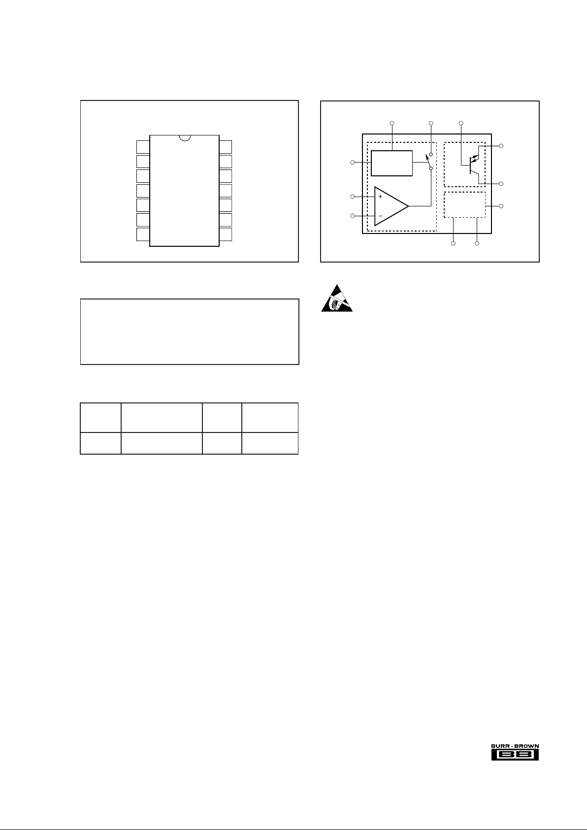
The SHC615 is available in SO-14 surface mount and
14-pin plastic DIPs, and is specified over the extended temperature range of –40°C to +85°C.
FEATURES
● PROPAGATION DELAY: 2.2ns
● BANDWIDTH: OTA: 750MHz
Comparator: 280MHz
● LOW INPUT BIAS CURRENT: –0.3µA
● SAMPLE/HOLD
SWITCHING TRANSIENTS: +1/–7mV
● SAMPLE/HOLD
FEEDTHROUGH REJECTION: 100dB
● CHARGE INJECTION: 40fC
● HOLD COMMAND DELAY TIME: 3.8ns
● TTL/CMOS HOLD CONTROL
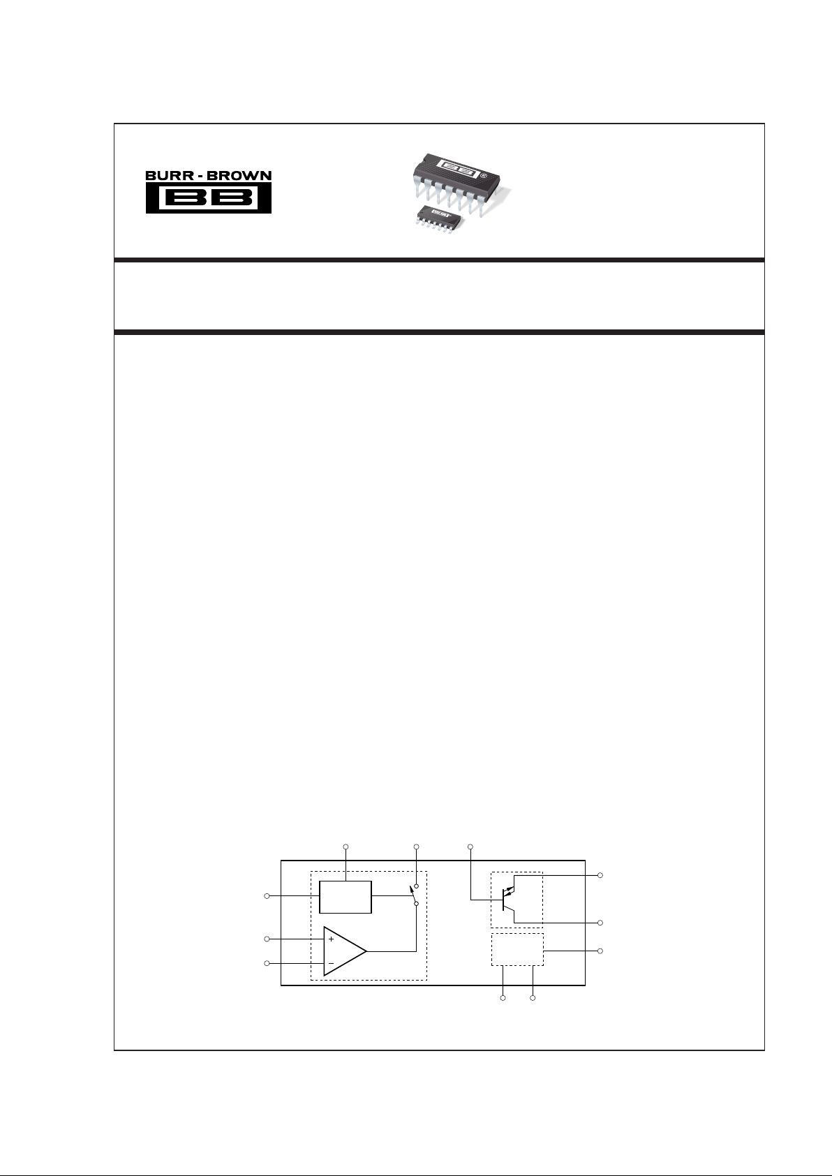
DESCRIPTION
The SHC615 is a complete subsystem for very fast
and precise DC restoration, offset clamping, and low
frequency hum suppression of wideband amplifiers or
buffers. Designed to stabilize the performance of
video signals, it can also be used as a sample/hold
amplifier, high-speed integrator, or peak detector for
nanosecond pulses. A wideband Operational
Transconductance Amplifier (OTA) with a high-impedance cascode current source output and fast sampling comparator set a new standard for high-speed
applications. Both can be used as stand-alone circuits
or combined to form a more complex signal processing stage. The self-biased, bipolar OTA can be viewed
as an ideal voltage-controlled current source and is
Switching
Stage
Biasing
SHC615
∞
SOTA
OTA
1
12
2
11
10
7
943
13 5
+V
CC–VCC
IQ Adjust
Collector (I
OUT
)
Emitter
C
HOLD
BaseGround
Hold Control
S/H
In+
S/H
In–
Sampling
Comparator (SC)
®
SHC615
SHC615
SHC615
International Airport Industrial Park • Mailing Address: PO Box 11400, Tucson, AZ 85734 • Street Address: 6730 S. Tucson Blvd., Tucson, AZ 85706 • Tel: (520) 746-1111 • Twx: 910-952-1111
Internet: http://www.burr-brown.com/ • FAXLine: (800) 548-6133 (US/Canada Only) • Cable: BBRCORP • Telex: 066-6491 • FAX: (520) 889-1510 • Immediate Product Info: (800) 548-6132
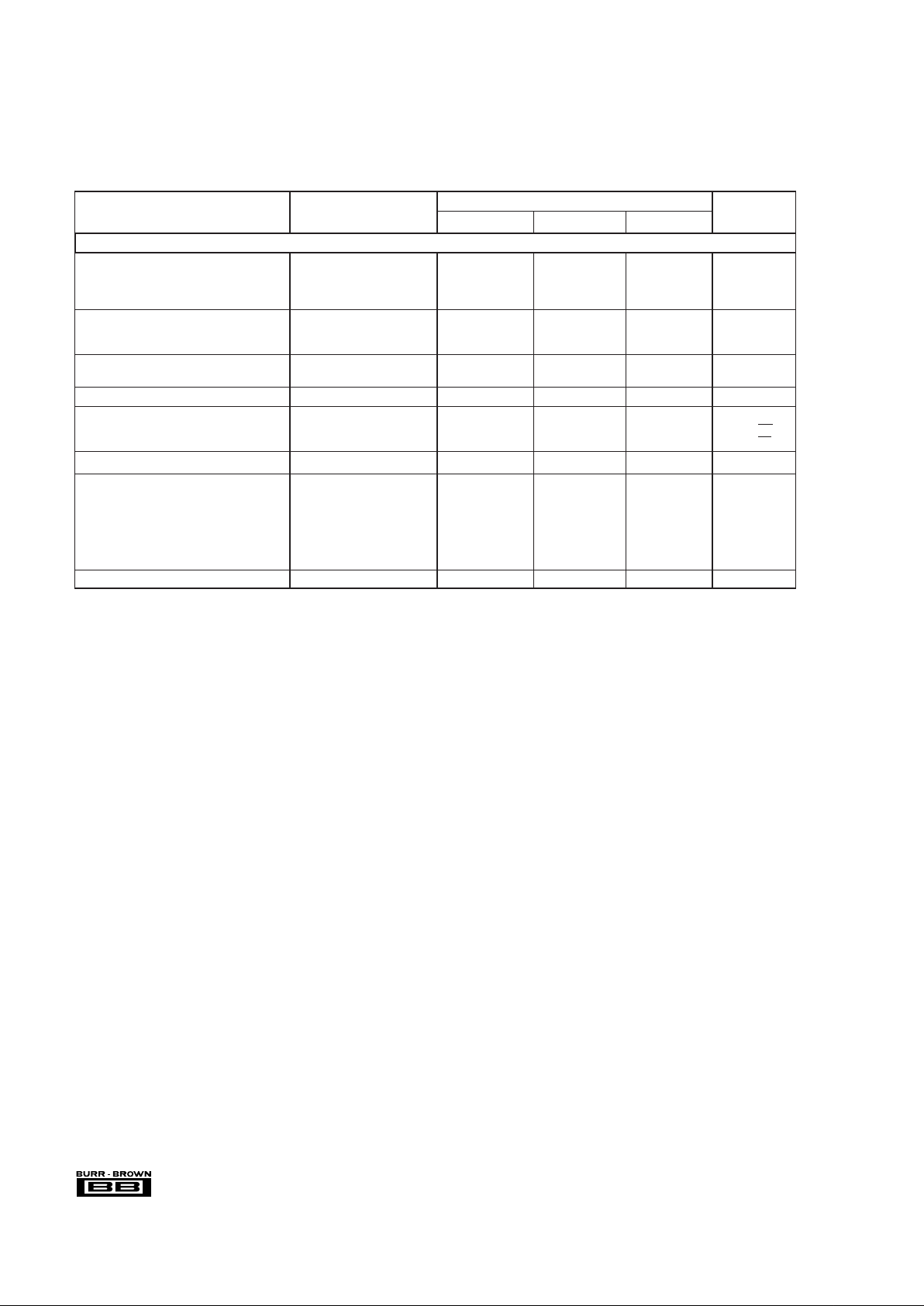
2
®
SHC615
SHC615AP, AU
PARAMETER CONDITIONS MIN TYP MAX UNITS
OTA
OFFSET VOLTAGE, V
E
at VB = 0
Initial 8 ±40 mV
vs Temperature 40 µV/°C
vs Supply (tracking) V
CC
= ±4.5V to ±5.5V 50 55 dB
B-INPUT BIAS CURRENT
Initial –0.3 ±0.9 µA
vs Temperature 1 nA/°C
C-OUTPUT BIAS CURRENT, I
C
at VB = 0
Initial –200 –77 +100 µA
B-INPUT IMPEDANCE 4.4 MΩ
INPUT NOISE
Voltage Noise Density, B-to-E f
OUT
= 100kHz to 100MHz 2.2 nV/√Hz
Voltage Noise Density, B-to-C f
OUT
= 100kHz to 100MHz 4.5 nV/√Hz
INPUT VOLTAGE RANGE ±3.4 V
OUTPUT
Output Voltage Compliance ±3.2 V
C-Current Output ±18 ±20 mA
E-Current Output ±18 ±20 mA
C-Output Impedance 0.5 MΩ
E-Output Impedance 12 Ω
Open-Loop Gain 96 dB
TRANSCONDUCTANCE Small Signal, <200mV 70 mA/V
The information provided herein is believed to be reliable; however, BURR-BROWN assumes no responsibility for inaccuracies or omissions. BURR-BROWN
assumes no responsibility for the use of this information, and all use of such information shall be entirely at the user’s own risk. Prices and specifications are
subject to change without notice. No patent rights or licenses to any of the circuits described herein are implied or granted to any third party. BURR-BROWN
does not authorize or warrant any BURR-BROWN product for use in life support devices and/or systems.
DC SPECIFICATIONS
At VCC = ±5V, R
LOAD
= 100Ω, RQ = 300Ω, RIN = 150Ω and TA = +25°C, unless otherwise specified.
3
®
SHC615
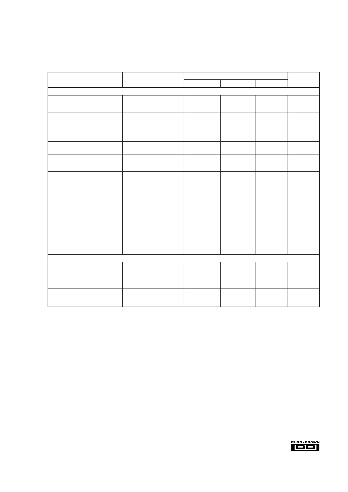
DC SPECIFICATIONS (CONT)
At VCC = ±5V, R
LOAD
= 1kΩ, RQ = 300Ω, and TA = +25°C, unless otherwise specified.
SHC615AP, AU
PARAMETER CONDITIONS MIN TYP MAX UNITS
COMPARATOR
INPUT BIAS CURRENT
Initial 1.0 ±5 µA
vs Temperature –2.3 nA/°C
C-OUTPUT BIAS CURRENT
Initial ±10 ±50 µA
vs Temperature ±13 nA/°C
INPUT IMPEDANCE
Input Impedance 0.2 MΩ
INPUT NOISE
Voltage Noise Density f
OUT
= 100kHz to 100MHz 5 nV/√Hz
INPUT VOLTAGE RANGE
Input Voltage Range ±3.0 V
Common-Mode Input Range ±3.2 V
OUTPUT
Output Voltage Compliance ±3.5 V
C-Current Output ±2.5 ±3.2 mA
C-Output Impedance 620 || 2 kΩ || pF
Open-Loop Gain 83 dB
TRANSCONDUCTANCE
Transconductance 22 mA/V
HOLD CONTROL
Logic 1 Voltage +2 +V
CC
+0.6 V
Logic 0 Voltage 0 0.8 V
Logic 1 Current V Hold Control = 5.0V 1 µA
Logic 0 Current V Hold Control = 0.8V 0.05 µA
TRANSFER CHARACTERISTICS
Charge Injection Track-To-Hold 40 fC
Feedthrough Rejection Hold Mode –100 dB
COMPLETE SHC615
POWER SUPPLY
Rated Voltage ±5V
Derated Performance ±4.5 ±5.5 V
Quiescent Current R
Q
= 300Ω±12 ±15 ±18 mA
Quiescent Current Range Programmable (Useful Range) ±3 to ±36 mA
TEMPERATURE RANGE
Operating –40 +85 °C
Storage –40 +125 °C
4
®
SHC615
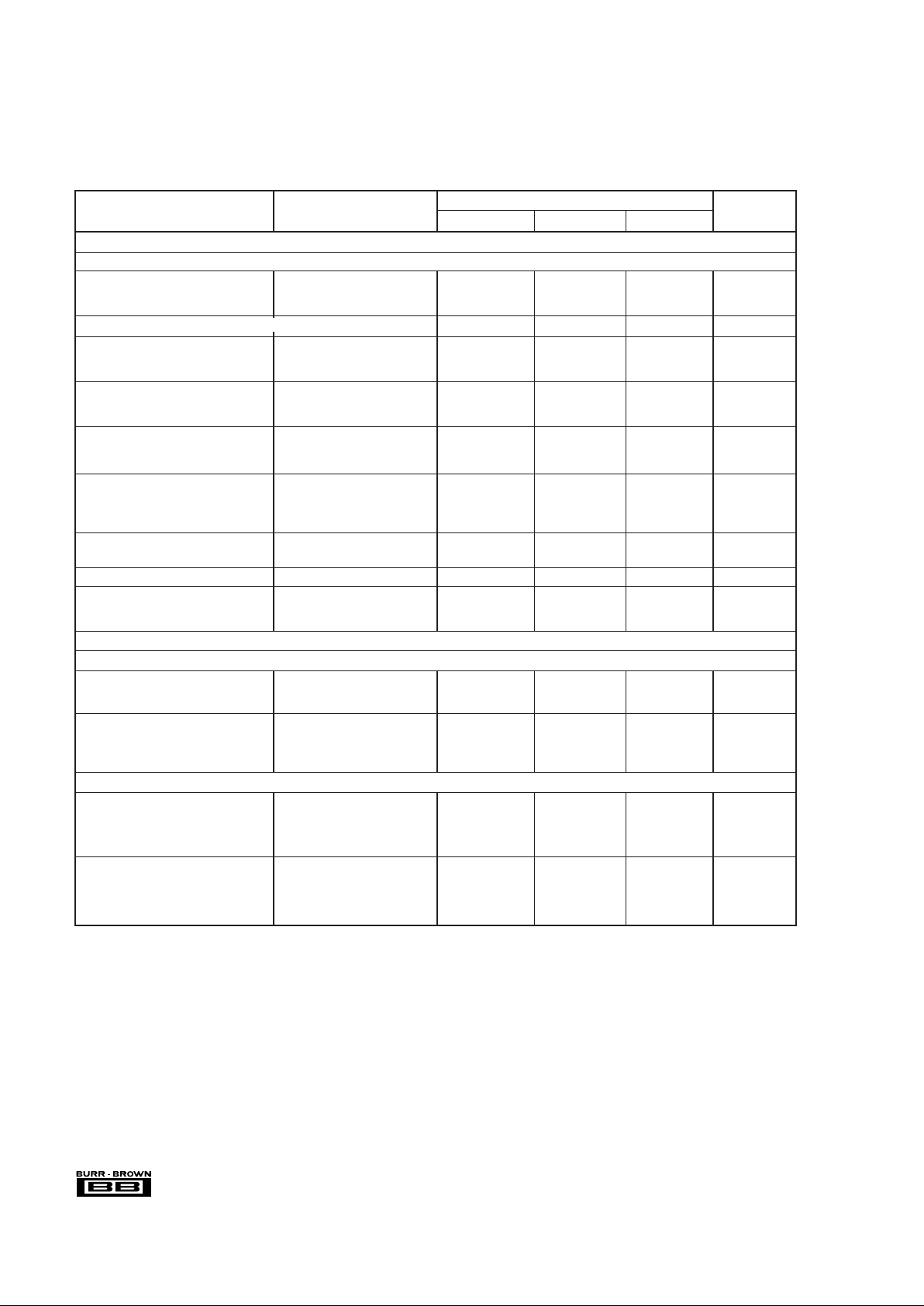
AC SPECIFICATIONS
At VCC = ±5V, R
LOAD
= 100Ω, R
SOURCE
= 50Ω, RQ = 300Ω, and TA = +25°C, unless otherwise specified.
SHC615AP, AU
PARAMETER CONDITIONS MIN TYP MAX UNITS
FREQUENCY DOMAIN
OTA
LARGE-SIGNAL BANDWIDTH V
OUT
= 5.0Vp-p 430 MHz
(–3dB), (B-to-E) V
OUT
= 2.8Vp-p 540 MHz
V
OUT
= 1.4Vp-p 620 MHz
SMALL-SIGNAL BANDWIDTH B-TO-E V
OUT
= 0.2Vp-p 520 MHz
DIFFERENTIAL GAIN (B-TO-E) f = 4.43MHz, V
OUT
= 0.7Vp-p,
R
L
= 150Ω 1.8 %
R
L
= 500Ω 0.1 %
DIFFERENTIAL PHASE f = 4.43MHz, V
OUT
= 0.7Vp-p,
R
L
= 150Ω 0.07 °
(B-to-E) R
L
= 500Ω 0.01 °
HARMONIC DISTORTION (B-TO-E) f = 30MHz, V
OUT
= 1.4Vp-p
Second Harmonic –50 dBc
Third Harmonic –46 dBc
LARGE SIGNAL BANDWIDTH
(–3dB), (B-to-C) V
OUT
= 5.0Vp-p 250 MHz
V
OUT
= 2.8Vp-p 580 MHz
V
OUT
= 1.4Vp-p 750 MHz
SMALL SIGNAL BANDWIDTH
B-to-C V
OUT
= 0.2Vp-p 680 MHz
COMPARATOR Sample Mode
BANDWIDTH I
OUT
= 4mAp-p 240 MHz
(–3dB) I
OUT
= 2mAp-p 270 MHz
I
OUT
= 1mAp-p 280 MHz
TIME DOMAIN
OTA
RISE TIME 2Vp-p Step, 10% to 90%
B-to-E 1.1 ns
B-to-C 1.2 ns
SLEW RATE 2Vp-p,B-to-E 1800 V/µs
B-to-C 1700 V/µs
5Vp-p,B-to-E 3300 V/µs
B-to-C 3000 V/µs
COMPARATOR
RISE TIME
10% to 90%, RL = 50Ω, I
OUT
= ±2mA
(Sample Mode) C
LOAD
= 1pF 2.5 ns
SLEW RATE
10% to 90%, RL = 50Ω, I
OUT
= ±2mA
(Sample Mode) C
LOAD
= 1pF 0.95 mA/ns
DYNAMIC CHARACTERISTICS
Propagation Delay Time t
PDH
, VOD = 200mV 2.2 ns
Propagation Delay Time t
PDL
, VOD = 200mV 2.15 ns
Delay Time Sample-to-Hold 3.8 ns
Hold-to-Sample 3.0 ns
5
®
SHC615
PIN CONFIGURATION
Top View DIP, SO-14
BLOCK DIAGRAM
IQ Adjust
Emitter, E
Base, B
C
HOLD
–V
CC
NC
Hold Control
NC
+V
CC
I
OUT
, Collector, C
S/H In–
S/H In+
Ground
NC
1
2
3
4
5
6
7
•
14
13
12
11
10
9
8
SHC615
Power Supply Voltage (±VCC)..............................................................±6V
Input Voltage
(1)
........................................................................ ±VCC ±0.7V
Operating Temperature ....................................................–40°C to +85°C
Storage Temperature ...................................................... –40°C to +125°C
Junction Temperature .................................................................... +150°C
Lead Temperature (soldering, 10s) ...............................................+300°C
Hold Control..............................................................–0.5V to +V
CC
+0.7V
NOTE: (1) Inputs are internally diode-clamped to ±V
CC
.
ABSOLUTE MAXIMUM RATINGS
ELECTROSTA TIC
DISCHARGE SENSITIVITY
Any integrated circuit can be damaged by ESD. Burr-Brown
recommends that all integrated circuits be handled with appropriate precautions. Failure to observe proper handling and
installation procedures can cause damage.
ESD damage can range from subtle performance degradation
to complete device failure. Precision integrated circuits may
be more susceptible to damage because very small parametric
changes could cause the device not to meet published specifications.
PACKAGE
DRAWING TEMPERATURE
PRODUCT PACKAGE NUMBER
(1)
RANGE
SHC615AP Plastic 14-Pin DIP 010 –40°C to +85°C
SHC615AU
SO 14-Lead Surface-Mount
235 –40°C to +85°C
NOTE: (1) For detailed drawing and dimension table, please see end of data
sheet, or Appendix C of Burr-Brown IC Data Book.
PACKAGE/ORDERING INFORMATION
Switching
Stage
Biasing
SHC615
∞
SOTA
OTA
1
12
2
11
10
7
943
13 5
+V
CC–VCC
IQ Adjust
Collector
(I
OUT
)
Emitter
C
HOLD
BaseGround
Hold
Control
S/H
In+
S/H
In–
Sampling
Comparator (SC)
6
®
SHC615
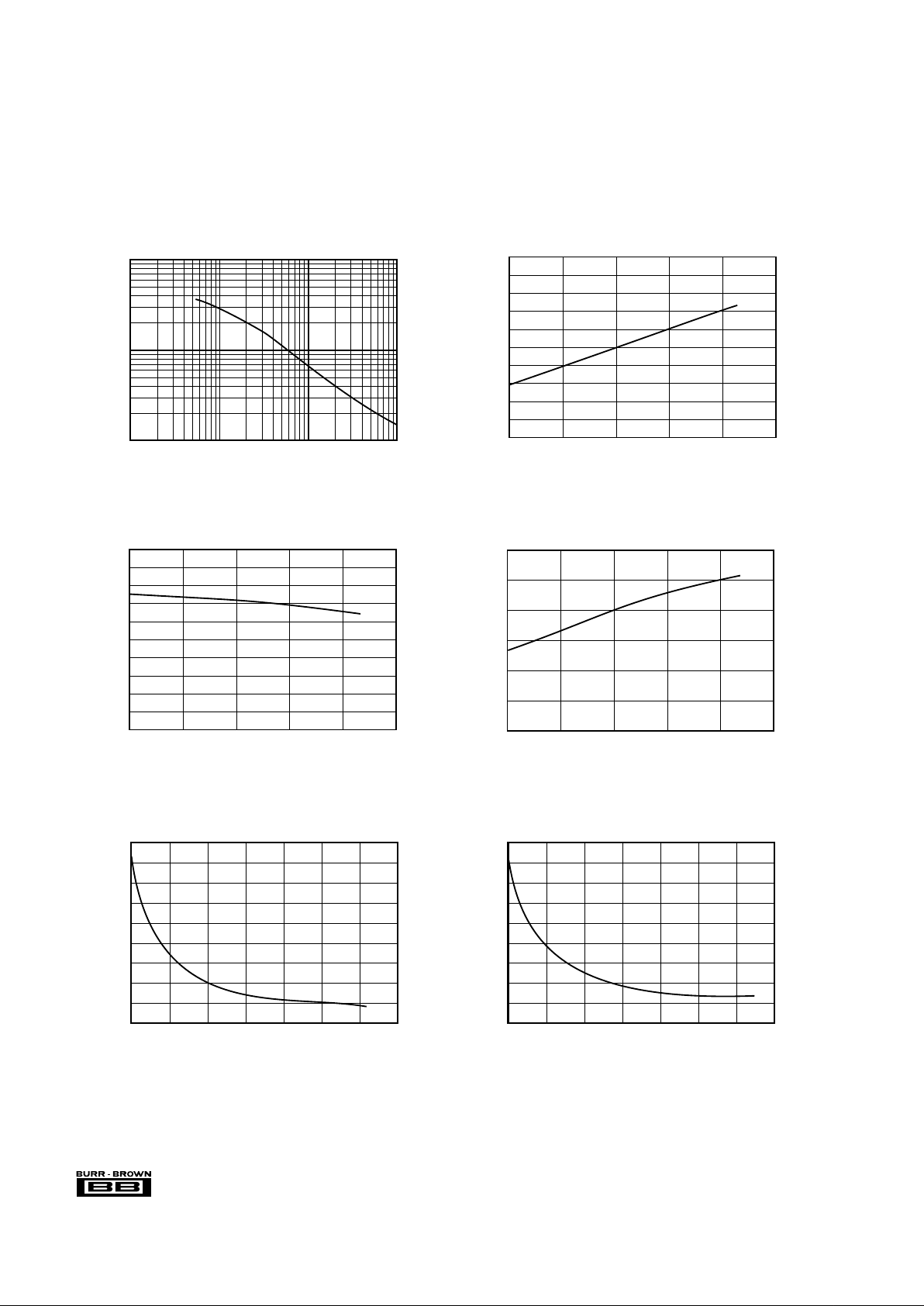
TYPICAL PERFORMANCE CURVES
At RQ = 300Ω, TA = +25°C, VCC = ±5V, unless otherwise noted.
OPERATIONAL TRANSCONDUCTANCE AMPLIFIER
SHC615 TOTAL QUIESCENT CURRENT vs R
Q
100
10
1
10 100 1000 10000
R
Q
(Ω)
Total Quiescent Current, I
Q
(mA)
TOTAL QUIESCENT CURRENT vs TEMPERATURE
1.50
1.40
1.30
1.20
1.10
1.00
0.90
0.80
0.70
0.60
0.50
–25 0 25 50 75 100
Temperature (C°)
Total Quiescent Current, I
Q
(Normalized)
OTA B-INPUT BIAS CURRENT vs TEMPERATURE
0.0
–0.1
–0.2
–0.3
–0.4
–0.5
–0.6
–0.7
–0.8
–0.9
–1.0
–25 0 25 50 75 100
Temperature (C°)
OTA-B Input Bias Current (µA)
OTA-B INPUT OFFSET VOLTAGE vs TEMPERATURE
12
10
8
6
4
2
0
–25 0 25 50 75 100
Temperature (C°)
OTA-B Input Offset Voltage (mV)
RE = 100Ω
OTA-B INPUT RESISTANCE vs
TOTAL QUIESCENT CURRENT
18
16
14
12
10
8
6
4
2
0
5 10152025303540
Total Quiescent Current, I
Q
(mA)
OTA-B Input Resistance (MΩ)
OTA-E OUTPUT RESISTANCE vs
TOTAL QUIESCENT CURRENT
45
40
35
30
25
20
15
10
5
0
4 9 14 19 24 29 34 39
Total Quiescent Current, I
Q
(mA)
OTA-E Output Resistance (Ω)
 Loading...