

Burr Brown SHC5320KH, SHC5320KP, SHC5320KU, SHC5320KU-1K, SHC5320SH Datasheet
1 SHC5320
®
SHC5320
FEATURES
● ACQUISITION TIME TO 0.01%: 1.5µs max
● HOLD MODE SETTLING TIME: 350ns max
● DROOP RATE AT +25°C: 0.5µV/µs max
● TTL COMPATIBLE
● FULL DIFFERENTIAL INPUTS
● INTERNAL HOLDING CAPACITOR
● TWO TEMPERATURE RANGES:
–40°C to +85°C (KH, KP, KU)
–55°C to +125°C (SH)
● PACKAGE OPTIONS: Ceramic and Plastic
DIP-14, SO-16
DESCRIPTION
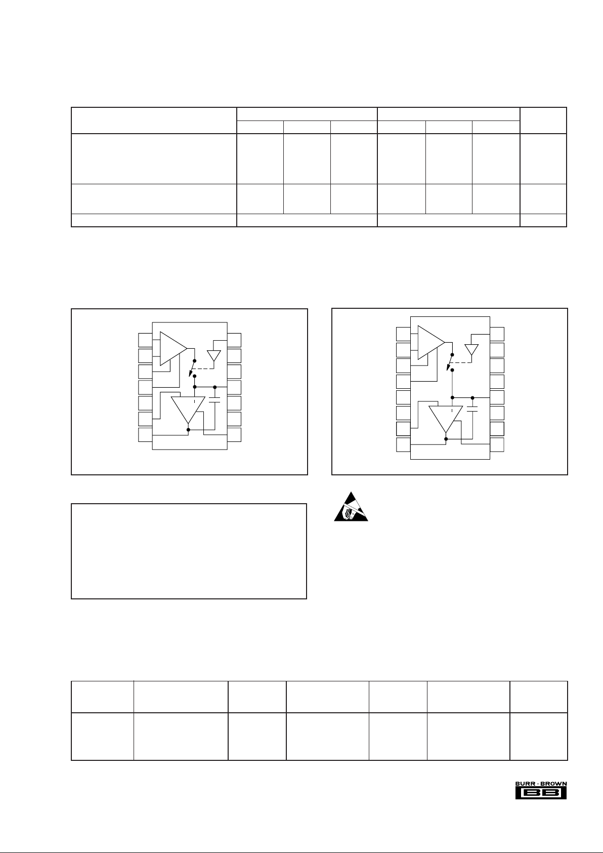
The SHC5320 is a bipolar, monolithic, sample/hold
circuit designed for use in precision, high-speed, dataacquisition applications.
The circuit employs an input transconductance amplifier capable of providing large amounts of charging
current to the holding capacitor, thus enabling fast
acquisition times. It also incorporates a low leakage
analog switch and an output integrating amplifier with
input bias current optimized to assure low droop rates.
Since the analog switch always drives into a load at
virtual ground, charge injection into the holding capacitor is constant over the entire input voltage range.
As a result, the charge offset (pedestal voltage) resulting from this charge injection can be adjusted to zero
by use of the offset adjustment capability. The device
includes an internal holding capacitor to simplify ease
of application; however, provision is also made to add
additional external capacitance to improve the output
voltage droop rate.
The SHC5320 is manufactured using a dielectric isolation process which minimizes stray capacitance (enabling higher-speed operation), and eliminates latchup associated with substrate SCRs. The SHC5320KH,
KP, and KU feature fully specified operation over the
extended industrial temperature range of –40°C to
+85°C, while the SHC5320SH operates over the temperature range of –55°C to +125°C. The device requires ±15V supplies for operation, and is packaged in
a reliable 14-pin ceramic or plastic dual-in-line package, as well as a 16-pin surface mount plastic package.
FPO
APPLICA TIONS
● PRECISION DATA ACQUISITION
SYSTEMS
● DIGITAL-TO-ANALOG CONVERTER
DEGLITCHER
● AUTO ZERO CIRCUITS
● PEAK DETECTORS
100pF
Output
Bandwidth
Control
Reference
Common
+
–
External
Hold
Capacitor
Offset
Adjust
–Input
+Input
Mode
Control
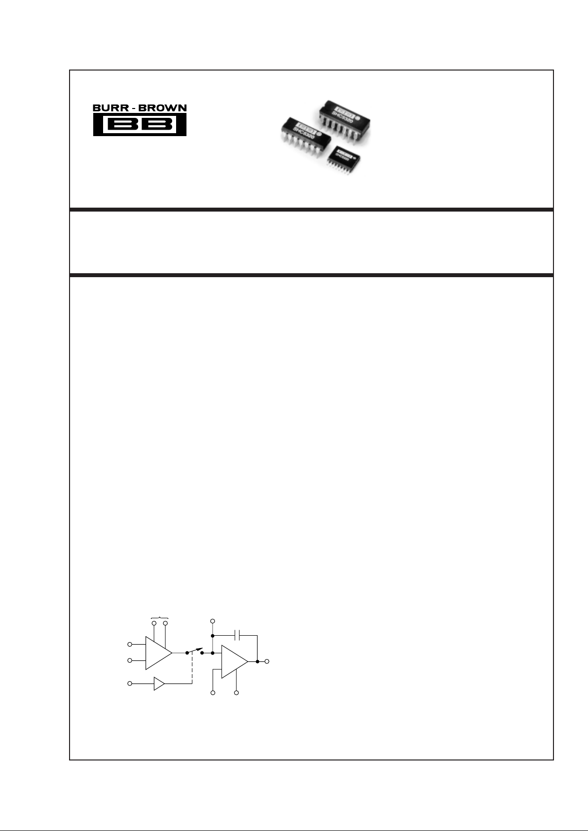
High-Speed, Bipolar, Monolithic
SAMPLE/HOLD AMPLIFIER
© 1985 Burr-Brown Corporation PDS-585G Printed in U.S.A. April, 2000
®
For most current data sheet and other product
information, visit www.burr-brown.com
International Airport Industrial Park • Mailing Address: PO Box 11400, Tucson, AZ 85734 • Street Address: 6730 S. Tucson Blvd., Tucson, AZ 85706 • Tel: (520) 746-1111
Twx: 910-952-1111 • Internet: http://www.burr-brown.com/ • Cable: BBRCORP • Telex: 066-6491 • FAX: (520) 889-1510 • Immediate Product Info: (800) 548-6132

2SHC5320
®
SPECIFICATIONS
At +25°C, rated power supplies, gain = +1, and with internal holding capacitor, unless otherwise noted.
SHC5320KH, KP, KU SHC5320SH
PARAMETERS MIN TYP MAX MIN TYP MAX UNITS
INPUT CHARACTERISTICS
ANALOG
Voltage Range ±10 ✻ V
Common-Mode Range ±10 ✻ V
Input Resistance 1 5 ✻✻ MΩ
Input Capacitance 3 ✻ pF
Bias Current ±100 ±300 ±70 ±200 nA
Bias Current Over Temperature Range ±300 ±200 nA
Offset Current ±30 ±300 ✻ ±100 nA
Offset Current Over Temperature Range ±300 ±100 nA
DIGITAL (Over Temperature Range)
V
IH
(Logic “1”) 2.0 ✻ V
V
IL
(Logic “0”) 0.8 ✻ V
I
IH
(VI = +5V) 0.1 ✻ µA
I
IL
(VI = 0V) 4 ✻ µA
Logic “0” = SAMPLE
Logic “1” = HOLD
OUTPUT CHARACTERISTICS
Voltage Range ±10 ✻ V
Current ±10 ✻ mA
Output Impedance (Hold Mode) 1 ✻ Ω
Noise, DC to 10MHz: Sample Hold 125 200 ✻✻µVrms
Hold Mode 125 200 ✻✻µVrms
DC ACCURACY/STABILITY
Gain, Open Loop, DC 3 x 10
5
2 x 10
6
10
6
✻ V/V
Input Offset Voltage ±0.5 ±0.2 mV
Input Offset Voltage Over Temperature Range ±1.5 ±2mV
Input Offset Voltage Drift ±5 ±20 ✻ ±15 µV/°C
CMRR
(1)
72 90 80 ✻ dB
Power Supply Rejection
(2)
:+V
CC
80 ✻ dB
–V
CC
65 ✻ dB
HOLD-TO-SAMPLE MODE
DYNAMIC CHARACTERISTICS
Acquisition Time, A = –1, 10V Step
(3)
:
to ±0.01% 1 1.5 ✻✻µs
to ±0.1% 0.8 1.2 ✻✻µs
SAMPLE MODE
Gain-Bandwidth Product (Gain = +1)
(4)
:
C
H
= 100pF 2 ✻ MHz
C
H
= 1000pF 180 ✻ kHz
Full Power Bandwidth
(5)
600 ✻ kHz
Slew Rate
(6)
45 ✻ V/µs
Rise Time
(4)
100 ✻ ns
Overshoot
(4)
15 ✻ %
SAMPLE-TO-HOLD MODE
DYNAMIC CHARACTERISTICS
Aperture Time
(7)
25 ✻ ns
Effective Aperture Time –50 –25 0 ✻✻✻ns
Aperture Uncertainty (Aperture Jitter) 0.3 ✻ ns
Charge Offset (Pedestal)
(8)
(Adjustable to Zero) 1 5 ✻✻mV
Charge Transfer
(8)
0.1 0.5 ✻✻pC
Sample-to-Hold Transient Settling Time
to ±0.01% of FSR 165 350 ✻✻ns
HOLD MODE
Droop
(9)
0.08 0.5 ✻✻µV/µs
Droop at Maximum Temperature
(9)
1.2 100 17 ✻ µV/µs
Drift Current
(9)
850 ✻✻pA
Drift Current at Maximum Temperature
(9)
0.12 10 1.7 ✻ nA
Feedthrough, 10Vp-p, 100kHz Sinewave 2 ✻ mV
The information provided herein is believed to be reliable; however, BURR-BROWN assumes no responsibility for inaccuracies or omissions. BURR-BROWN assumes
no responsibility for the use of this information, and all use of such information shall be entirely at the user’s own risk. Prices and specifications are subject to change
without notice. No patent rights or licenses to any of the circuits described herein are implied or granted to any third party. BURR-BROWN does not authorize or warrant
any BURR-BROWN product for use in life support devices and/or systems.
3 SHC5320
®
Hermetic Ceramic
Top View DIP
+
1
2
3
4
5
6
7
14
13
12
11
10
9
8
–Input
+Input
Offset Adjustment
Offset Adjustment
–V
CC
Reference
Common
Output
Mode Control
Supply Common
NC
External Hold
Capacitor
NC
+V
CC
Bandwidth Control
SHC5320KH, KP
SHC5320KU
1
2
3
4
5
6
7
8
16
15
14
13
12
11
10
9
–Input
+Input
Offset Adjustment
Offset Adjustment
NC
–V
CC
Reference
Common
Output
Mode Control
Supply Common
NC
NC
External Hold
Capacitor
NC
+V
CC
Bandwidth Control
+
PIN CONNECTIONS
Voltage Between +VCC and –VCC Terminals ......................................... 40V
Input Voltage........................................................... Actual Supply Voltage
Differential Input Voltage ................................................................... ±24V
Digital Input Voltage.................................................................. +15V, –1V
Output Current, continuous
(2)
......................................................... ±20mA
Internal Power Dissipation ............................................................. 450mW
Storage Temperature Range .................................... –65°C < T
A
< +150°C
Output Short-Circuit Duration
(3)
.........................................................None
Lead Temperature (soldering, 10s) ................................................. 300°C
CAUTION: These devices are sensitive to electrostatic discharge.
Appropriate I.C. handling procedures should be followed.
NOTES: (1) Absolute maximum ratings are limiting values, applied individually,
beyond which the serviceability of the circuit may be impaired. Functional
operation under any of these conditions is not necessarily implied. Absolute
maximum ratings apply to both dice and package parts, unless otherwise noted.
(2) Internal power dissipation may limit output current to less than +20mA. (3)
WARNING: This device cannot withstand even a momentary short circuit
to either supply.
ABSOLUTE MAXIMUM RATINGS
(1)
Top View SO
SPECIFICATIONS (Cont.)
At +25°C, rated power supplies, gain = +1, and with internal holding capacitor, unless otherwise noted.
SHC5320KH, KP, KU SHC5320SH
PARAMETERS MIN TYP MAX MIN TYP MAX UNITS
POWER SUPPLIES
+V
CC
+12 +15 +18 ✻✻✻V
–V
CC
–12 –15 –18 ✻✻✻V
+I
CC
(+VCC = 15V)
(9)
11 13 ✻✻mA
–I
CC
(–VCC = 15V)
(9)
–11 –13 ✻✻mA
TEMPERATURE
Specification –40 +85 –55 +125 °C
Storage –65 +150 ✻✻°C
PACKAGE Hermetic Ceramic, Plastic DIP, SO
✻ Specification the same as SCH5320KH, KP, KU.
NOTES: (1) V
CM
= ±5VDC. (2) Based on a ±0.5V swing for each supply with all other supplies held constant. (3) VO = 10V step, RL = 2kΩ, CL = 50pF. (4) VO = 200mVp-p,
R
L
= 2kΩ, CL = 50pF. (5) VIN = 20Vp-p, RL = 2kΩ, CL = 50pF, unattenuated output. (6) VO = 20V step, RL = 2kΩ, CL = 50pF. (7) Simulated only, not tested. (8) VIN =
0V, V
IH
= +3.5V, tR < 20ns (VIL to VIH). (9) Specified for zero differential input voltage between pins 1 and 2. Supply current will increase with differential input (as may
occur in the Hold mode) to approximately ±28mA average at 20V differential.
PACKAGE SPECIFIED
DRAWING TEMPERATURE PACKAGE ORDERING TRANSPORT
PRODUCT PACKAGE NUMBER RANGE MARKING NUMBER
(1)
MEDIA
SHC5320KH CERDIP-14 163 –40°C to +85°C SHC5320KH SHC5320KH Rail
SHC5320KP DIP-14 010 –40°C to +85°C SHC5320KP SHC5320KP Rail
SHC5320KU SO-16 211 –40°C to +85°C SHC5320KU SHC5320KU Rail
""""SHC5320KU SHC5320KU/1K Tape and Reel
SHC5320SH CERDIP-14 163 –55°C to +125°C SHC5320SH SHC5320SH Rail
NOTE: (1) Models with a slash (/) are available only in Tape and Reel in the quantities indicated (e.g., /1K indicates 1000 devices per reel). Ordering 1000 pieces
of “SHC5320KU/1K” will get a single 1000-piece Tape and Reel.
PACKAGE/ORDERING INFORMATION
ELECTROSTATIC
DISCHARGE SENSITIVITY
This integrated circuit can be damaged by ESD. Burr-Brown
recommends that all integrated circuits be handled with
appropriate precautions. Failure to observe proper handling
and installation procedures can cause damage.
ESD damage can range from subtle performance degradation to complete device failure. Precision integrated circuits
may be more susceptible to damage because very small
parametric changes could cause the device not to meet its
published specifications.
 Loading...