

Page 1
查询SHC5320供应商
®
FPO
For most current data sheet and other product
information, visit www.burr-brown.com
High-Speed, Bipolar, Monolithic
SAMPLE/HOLD AMPLIFIER
FEATURES
● ACQUISITION TIME TO 0.01%: 1.5µs max
● HOLD MODE SETTLING TIME: 350ns max
● DROOP RATE AT +25°C: 0.5µV/µs max
● TTL COMPATIBLE
● FULL DIFFERENTIAL INPUTS
● INTERNAL HOLDING CAPACITOR
● TWO TEMPERATURE RANGES:
–40°C to +85°C (KH, KP, KU)
–55°C to +125°C (SH)
● PACKAGE OPTIONS: Ceramic and Plastic
DIP-14, SO-16
APPLICA TIONS
● PRECISION DATA ACQUISITION
SYSTEMS
● DIGITAL-TO-ANALOG CONVERTER
DEGLITCHER
● AUTO ZERO CIRCUITS
● PEAK DETECTORS
Offset
Adjust
–Input
+Input
Mode
Control
External
Hold
Capacitor
100pF
–
+
Output
SHC5320
DESCRIPTION
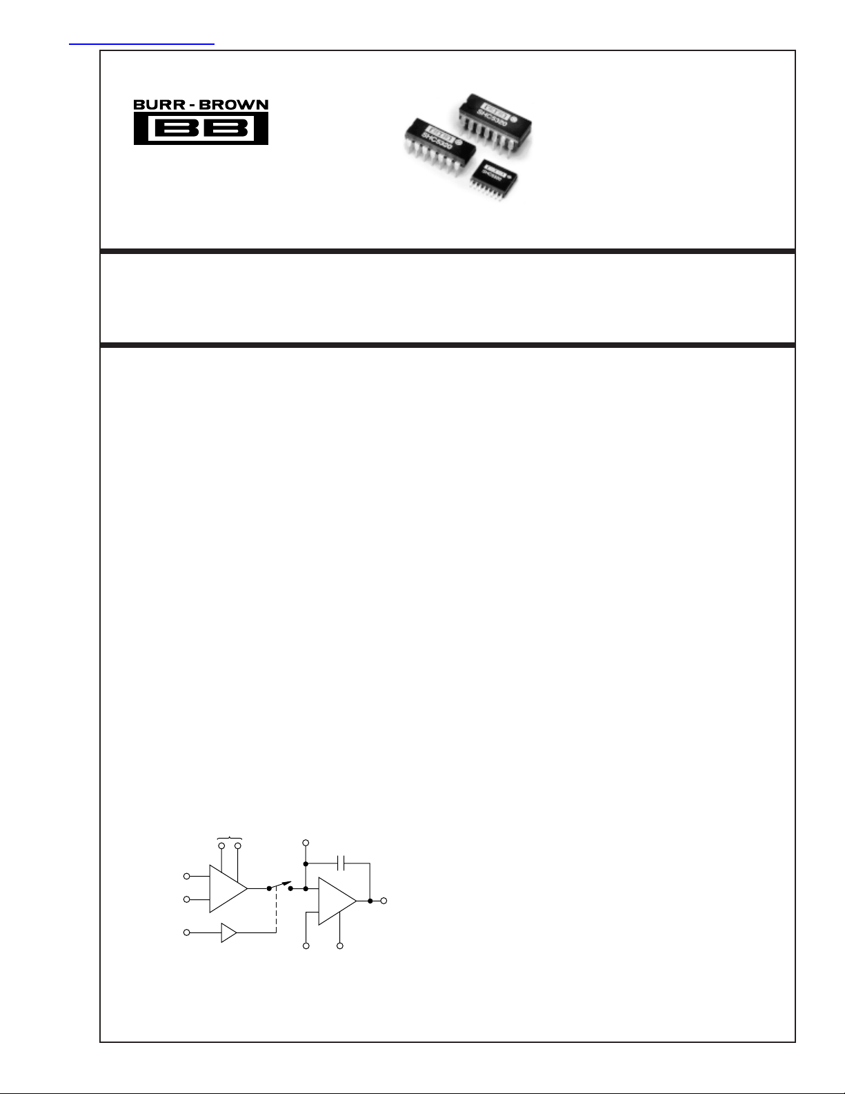
The SHC5320 is a bipolar, monolithic, sample/hold
circuit designed for use in precision, high-speed, dataacquisition applications.
The circuit employs an input transconductance amplifier capable of providing large amounts of charging
current to the holding capacitor, thus enabling fast
acquisition times. It also incorporates a low leakage
analog switch and an output integrating amplifier with
input bias current optimized to assure low droop rates.
Since the analog switch always drives into a load at
virtual ground, charge injection into the holding capacitor is constant over the entire input voltage range.
As a result, the charge offset (pedestal voltage) resulting from this charge injection can be adjusted to zero
by use of the offset adjustment capability. The device
includes an internal holding capacitor to simplify ease
of application; however, provision is also made to add
additional external capacitance to improve the output
voltage droop rate.
The SHC5320 is manufactured using a dielectric isolation process which minimizes stray capacitance (enabling higher-speed operation), and eliminates latchup associated with substrate SCRs. The SHC5320KH,
KP, and KU feature fully specified operation over the
extended industrial temperature range of –40°C to
+85°C, while the SHC5320SH operates over the temperature range of –55°C to +125°C. The device requires ±15V supplies for operation, and is packaged in
a reliable 14-pin ceramic or plastic dual-in-line package, as well as a 16-pin surface mount plastic package.
Reference
Common
International Airport Industrial Park • Mailing Address: PO Box 11400, Tucson, AZ 85734 • Street Address: 6730 S. Tucson Blvd., Tucson, AZ 85706 • Tel: (520) 746-1111
Twx: 910-952-1111 • Internet: http://www.burr-brown.com/ • Cable: BBRCORP • Telex: 066-6491 • FAX: (520) 889-1510 • Immediate Product Info: (800) 548-6132
© 1985 Burr-Brown Corporation PDS-585G Printed in U.S.A. April, 2000
Bandwidth
Control
1 SHC5320
®
Page 2
SPECIFICATIONS
At +25°C, rated power supplies, gain = +1, and with internal holding capacitor, unless otherwise noted.
SHC5320KH, KP, KU SHC5320SH
PARAMETERS MIN TYP MAX MIN TYP MAX UNITS
INPUT CHARACTERISTICS
ANALOG
Voltage Range ±10 ✻ V
Common-Mode Range ±10 ✻ V
Input Resistance 1 5 ✻✻ MΩ
Input Capacitance 3 ✻ pF
Bias Current ±100 ±300 ±70 ±200 nA
Bias Current Over Temperature Range ±300 ±200 nA
Offset Current ±30 ±300 ✻ ±100 nA
Offset Current Over Temperature Range ±300 ±100 nA
DIGITAL (Over Temperature Range)
(Logic “1”) 2.0 ✻ V
V
IH
(Logic “0”) 0.8 ✻ V
V
IL
(VI = +5V) 0.1 ✻ µA
I
IH
(VI = 0V) 4 ✻ µA
I
IL
Logic “0” = SAMPLE
Logic “1” = HOLD
OUTPUT CHARACTERISTICS
Voltage Range ±10 ✻ V
Current ±10 ✻ mA
Output Impedance (Hold Mode) 1 ✻ Ω
Noise, DC to 10MHz: Sample Hold 125 200 ✻✻µVrms
DC ACCURACY/STABILITY
Gain, Open Loop, DC 3 x 10
Input Offset Voltage ±0.5 ±0.2 mV
Input Offset Voltage Over Temperature Range ±1.5 ±2mV
Input Offset Voltage Drift ±5 ±20 ✻ ±15 µV/°C
(1)
CMRR
Power Supply Rejection
HOLD-TO-SAMPLE MODE
DYNAMIC CHARACTERISTICS
Acquisition Time, A = –1, 10V Step
to ±0.01% 1 1.5 ✻✻µs
to ±0.1% 0.8 1.2 ✻✻µs
SAMPLE MODE
Gain-Bandwidth Product (Gain = +1)
= 100pF 2 ✻ MHz
C
H
= 1000pF 180 ✻ kHz
C
H
Full Power Bandwidth
Slew Rate
Rise Time
Overshoot
(6)
(4)
(4)
SAMPLE-TO-HOLD MODE
DYNAMIC CHARACTERISTICS
Aperture Time
Effective Aperture Time –50 –25 0 ✻✻✻ns
Aperture Uncertainty (Aperture Jitter) 0.3 ✻ ns
Charge Offset (Pedestal)
Charge Transfer
Sample-to-Hold Transient Settling Time
to ±0.01% of FSR 165 350 ✻✻ns
HOLD MODE
(9)
Droop
Droop at Maximum Temperature
Drift Current
(9)
Drift Current at Maximum Temperature
Feedthrough, 10Vp-p, 100kHz Sinewave 2 ✻ mV
Hold Mode 125 200 ✻✻µVrms
5
(2)
:+V
CC
–V
CC
(3)
:
(4)
:
(5)
72 90 80 ✻ dB
80 ✻ dB
65 ✻ dB
2 x 10
6
6
10
✻ V/V
600 ✻ kHz
45 ✻ V/µs
100 ✻ ns
15 ✻ %
(7)
(8)
(8)
(Adjustable to Zero) 1 5 ✻✻mV
(9)
(9)
25 ✻ ns
0.1 0.5 ✻✻pC
0.08 0.5 ✻✻µV/µs
1.2 100 17 ✻ µV/µs
850 ✻✻pA
0.12 10 1.7 ✻ nA
The information provided herein is believed to be reliable; however, BURR-BROWN assumes no responsibility for inaccuracies or omissions. BURR-BROWN assumes
no responsibility for the use of this information, and all use of such information shall be entirely at the user’s own risk. Prices and specifications are subject to change
without notice. No patent rights or licenses to any of the circuits described herein are implied or granted to any third party. BURR-BROWN does not authorize or warrant
any BURR-BROWN product for use in life support devices and/or systems.
®
2SHC5320
Page 3
1
2
3
4
5
6
7
8
16
15
14
13
12
11
10
9
–Input
+Input
Offset Adjustment
Offset Adjustment
NC
–V
CC
Reference
Common
Output
Mode Control
Supply Common
NC
NC
External Hold
Capacitor
NC
+V
CC
Bandwidth Control
+
SPECIFICATIONS (Cont.)
At +25°C, rated power supplies, gain = +1, and with internal holding capacitor, unless otherwise noted.
SHC5320KH, KP, KU SHC5320SH
PARAMETERS MIN TYP MAX MIN TYP MAX UNITS
POWER SUPPLIES
+V
CC
–V
CC
(+VCC = 15V)
+I
CC
(–VCC = 15V)
–I
CC
TEMPERATURE
Specification –40 +85 –55 +125 °C
Storage –65 +150 ✻✻°C
PACKAGE Hermetic Ceramic, Plastic DIP, SO
✻ Specification the same as SCH5320KH, KP, KU.
NOTES: (1) V
= 2kΩ, CL = 50pF. (5) VIN = 20Vp-p, RL = 2kΩ, CL = 50pF, unattenuated output. (6) VO = 20V step, RL = 2kΩ, CL = 50pF. (7) Simulated only, not tested. (8) VIN =
R
L
= +3.5V, tR < 20ns (VIL to VIH). (9) Specified for zero differential input voltage between pins 1 and 2. Supply current will increase with differential input (as may
0V, V
IH
occur in the Hold mode) to approximately ±28mA average at 20V differential.
(9)
(9)
= ±5VDC. (2) Based on a ±0.5V swing for each supply with all other supplies held constant. (3) VO = 10V step, RL = 2kΩ, CL = 50pF. (4) VO = 200mVp-p,
CM
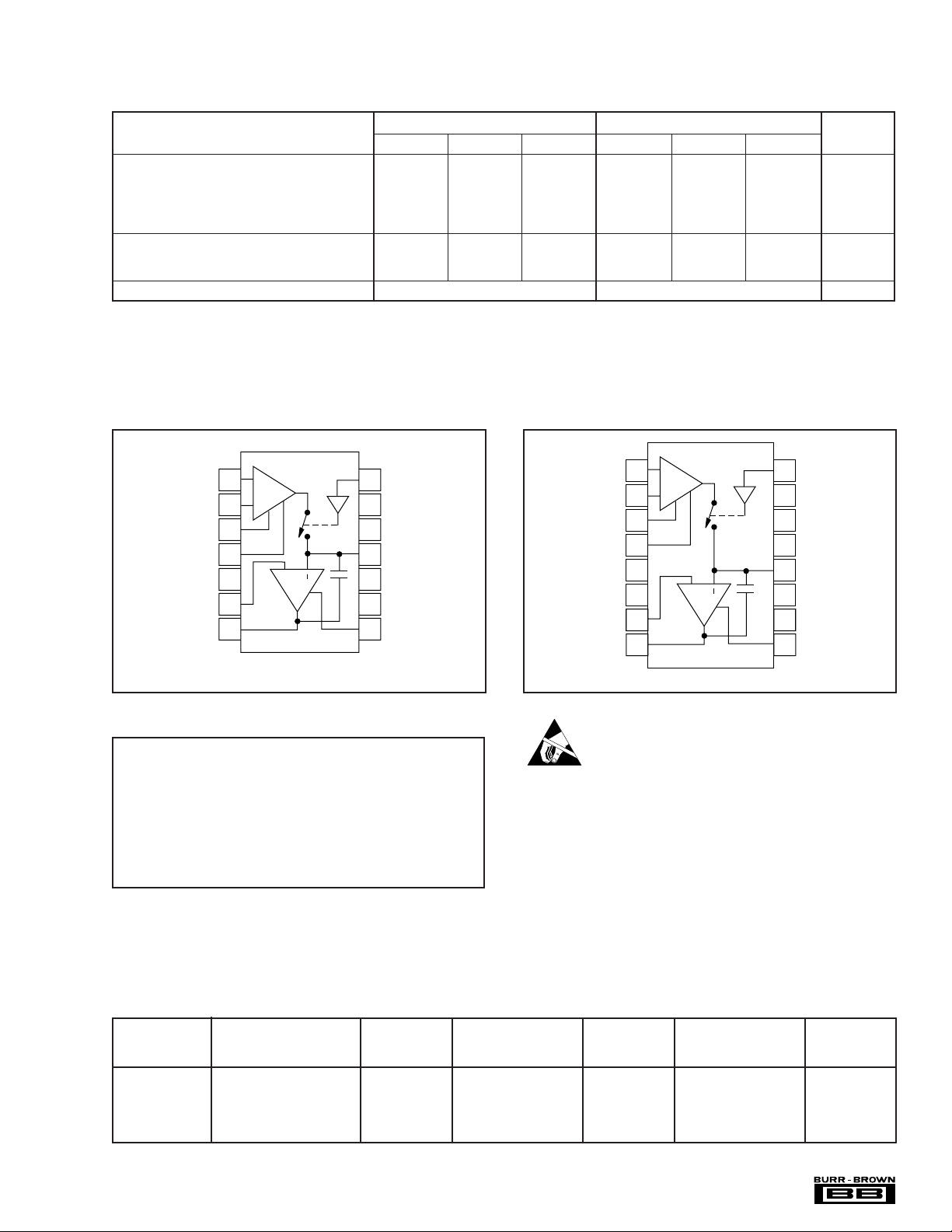
PIN CONNECTIONS
Top View DIP
1
–Input
2
+Input
–V
3
4
5
CC
6
7
+
Offset Adjustment
Offset Adjustment
Reference
Common
Output
+12 +15 +18 ✻✻✻V
–12 –15 –18 ✻✻✻V
Mode Control
14
Supply Common
13
NC
12
External Hold
11
Capacitor
NC
10
+V
9
CC
Bandwidth Control
8
11 13 ✻✻mA
–11 –13 ✻✻mA
Hermetic Ceramic
Top View SO
SHC5320KH, KP
SHC5320KU
ABSOLUTE MAXIMUM RATINGS
Voltage Between +VCC and –VCC Terminals ......................................... 40V
Input Voltage........................................................... Actual Supply Voltage
Differential Input Voltage ................................................................... ±24V
Digital Input Voltage.................................................................. +15V, –1V
Output Current, continuous
Internal Power Dissipation ............................................................. 450mW
Storage Temperature Range .................................... –65°C < T
Output Short-Circuit Duration
Lead Temperature (soldering, 10s) ................................................. 300°C
CAUTION: These devices are sensitive to electrostatic discharge.
Appropriate I.C. handling procedures should be followed.
NOTES: (1) Absolute maximum ratings are limiting values, applied individually,
beyond which the serviceability of the circuit may be impaired. Functional
operation under any of these conditions is not necessarily implied. Absolute
maximum ratings apply to both dice and package parts, unless otherwise noted.
(2) Internal power dissipation may limit output current to less than +20mA. (3)
WARNING: This device cannot withstand even a momentary short circuit
to either supply.
(2)
......................................................... ±20mA
(3)
.........................................................None
(1)
ELECTROSTATIC
DISCHARGE SENSITIVITY
This integrated circuit can be damaged by ESD. Burr-Brown
< +150°C
A
recommends that all integrated circuits be handled with
appropriate precautions. Failure to observe proper handling
and installation procedures can cause damage.
ESD damage can range from subtle performance degradation to complete device failure. Precision integrated circuits
may be more susceptible to damage because very small
parametric changes could cause the device not to meet its
published specifications.
PACKAGE/ORDERING INFORMATION
PRODUCT PACKAGE NUMBER RANGE MARKING NUMBER
SHC5320KH CERDIP-14 163 –40°C to +85°C SHC5320KH SHC5320KH Rail
SHC5320KP DIP-14 010 –40°C to +85°C SHC5320KP SHC5320KP Rail
SHC5320KU SO-16 211 –40°C to +85°C SHC5320KU SHC5320KU Rail
""""SHC5320KU SHC5320KU/1K Tape and Reel
SHC5320SH CERDIP-14 163 –55°C to +125°C SHC5320SH SHC5320SH Rail
NOTE: (1) Models with a slash (/) are available only in Tape and Reel in the quantities indicated (e.g., /1K indicates 1000 devices per reel). Ordering 1000 pieces
of “SHC5320KU/1K” will get a single 1000-piece Tape and Reel.
PACKAGE SPECIFIED
DRAWING TEMPERATURE PACKAGE ORDERING TRANSPORT
(1)
MEDIA
3 SHC5320
®
Page 4

TYPICAL PERFORMANCE CURVES
q
)
±VCC = 15V.
TYPICAL SAMPLE/HOLD PERFORMANCE
AS FUNCTION OF HOLDING CAPACITOR
10
5
1.0
Acquisition Time (µs)
for 10V Step to ±0.01%
Voltage Droop (mV/100ms)
during Hold Mode
0.5
0.1
0.05
Charge Offset
0.01
Error (mV)
100 1000 10 100 1M
C Value (pF)
H
OPEN-LOOP GAIN
AND PHASE RESPONSE
120
100
80
60
Gain (dB)
40
G
CH = 1100pF
θ
CH = 100pF
G
20
–45
0
45
90
135
180
Hold Step Voltage (mV)
DRIFT
I (pA)
Phase (degrees)
CHARGE OFFSET
vs MODE CONTROL (V ) VOLTAGE
IH
2.0
C = 100pF
H
1.5
+75°C
1.0
+25°C
0.5
0
12345
Logic Level High (V)
DRIFT CURRENT
10k
vs TEMPERATURE
1k
C = 100pF
H
100
10
1
0
1
10 100 1k 10k 100k 1M 10M
Fre
uency (Hz
225
0
–25 0 25 50
–50
Temperature (°C)
75
100 125
®
4SHC5320
Page 5

Input
Feed-
though
Output
Slew Rate
Limited
Settling
Time
SampleMode ControlSample
Offset
Aperture Time
Hold
Acquisition
Time
Aperture
Uncertainty
Droop
Settling
Time
Sample-to-Hold
Transient and
Charge Offset
DISCUSSION OF
SPECIFICATIONS
WHAT IS A SAMPLE/HOLD AMPLIFIER?
A sample/hold amplifier (also sometimes called a track-andhold amplifier) is a circuit that captures and holds an analog
voltage at a specific point in time under control of an
external circuit, such as a microprocessor. This type of
circuit has many applications; however, its primary use is in
data acquisition systems which require that the voltage be
captured and held during the analog-to-digital conversion
process. Use of a sample/hold effectively increases the
bandwidth of a data acquisition system by a significant
amount. For further discussion of this capability, refer to
“Signal Digitization” in the Applications section of this data
sheet.
The ideal sample/hold amplifier in its simplest form contains
four primary components as illustrated in Figure 1, although
in actual practice they may not be internally connected
exactly as shown. Amplifier A1, the input buffer, provides a
high impedance load to the source circuit and supplies
charging current to the holding capacitor CH. Switch S
opens and closes under external control to gate the buffered
input signal to the holding circuit or to remove it so that the
most recently sampled signal will be held. Amplifier A
serves to present a high impedance load to the holding
capacitor and to provide a low impedance voltage source for
external loads. A minimum of three terminals are provided
for the user: input, output, and mode control (or sample/hold
control). When S1, is closed, the output signal follows the
input signal, subject to errors imposed by amplifier bandwidth and other errors as discussed below. When S1, is
opened, the voltage stored on the holding capacitor will be
held indefinitely (in the ideal case), and will appear at the
output of the circuit until S1, is again closed under command
of the mode control signal.
–
+
C
A
2
Output
H
S
1
Input
Mode
Control
–
A
1
+
FIGURE 1. Ideal Sample/Hold Amplifier.
The following discussion of specifications covers the critical
types of errors which may be experienced in applications of
a sample/hold amplifier. These errors are depicted graphically in Figure 2, and in the Typical Performance Curves.
Acquisition Time is the time required for the sample/hold
output to settle within a given error band of its final value
after the sample mode is initiated. Included in this time are
effects of switch delay time, slew rate of the buffer amplifier, and settling time for a specified change in held voltage
value. Slew rate limitations of the buffer amplifier will cause
FIGURE 2. Illustration of Sample/Hold Specifications.
actual acquisition time to be highly dependent on the amplitude of the voltage to be acquired, relative to the value
already held by the capacitor. Therefore, proper specification of sample/hold amplifier performance includes definition of both output value step size and required error band
accuracy.
Aperture Time (or aperture delay time) is the time required
1
for switch S1, to open and remove the charging signal from
the capacitor after the mode control signal has changed from
“sample” to “hold.” This time is measured from the 50%
2
point of the Hold mode transition to the time at which the
output stops tracking the input. This parameter is very
important in applications for which the input signal is
changing very rapidly when the Hold mode is initiated.
Effective Aperture Time is the difference in propagation
delay times of the analog signal and the mode control signal
from their respective input pins to switch S1. This time may
be negative, zero, or positive. A negative value indicates that
the mode control propagation delay is shorter than the
analog propagation delay, with the result that the analog
value present on the capacitor at the time the switch opens
occurred earlier than the application of the mode control
signal by the amount of the effective aperture delay time.
Aperture Uncertainty (or aperture jitter) is the variation
observed in the aperture time over a large number of observations. This parameter is important when the analog input
is a rapidly changing signal, as aperture uncertainty contributes to lack of knowledge (at the output) about the true value
of the input at the precise time the Hold mode is initiated.
The maximum input frequency for a given acceptable error
contribution due to aperture uncertainty is
f
= Maximum Fractional Error/2πt
MAX
where Maximum Fractional Error (MFE) is the ratio of the
maximum allowable error voltage to peak voltage, and tU is
the aperture uncertainty time. For a bipolar ±10V signal and
a maximum uncertainty error of 1/2LSB in a 12-bit system,
the MFE is equal to 1/2LSB ÷ V
= 2.44mV ÷ 10V =
PEAK
0.000244V/V, since 1/2LSB = 2.44mV for a 20V full-scale
range.
For the same system operating with a unipolar 0V to 10V
signal, MFE would be 0.000122V/V.
5 SHC5320
U
®
Page 6

Charge Offset (pedestal) is the output voltage change that
results from charge transfer into the hold capacitor through
stray capacitance when the Hold mode command is given.
This charge appears as an offset voltage at the output, and in
some sample/hold amplifiers may be a function of the input
voltage.
Charge offset is specified for the SHC5320 using only the
internal holding capacitor. When an external capacitor is
added, charge offset is calculated as Charge Transfer (pC)
divided by total hold capacitance. Charge Transfer is also
specified for the SHC5320, and total hold capacitance is the
sum of the internal hold capacitor value (100pF) and the
external hold capacitor. Since charge transfer is not a function of analog input voltage for the SHC5320, this error may
be removed by means of the offset adjustment capability of
the amplifier.
Droop Rate is the change in output voltage over time during
the Hold mode as a result of hold capacitor leakage, switch
leakage, and bias current of the output amplifier. Droop rate
varies with temperature and the quality of the external
holding capacitor, if used. Careful circuit layout is also
required to minimize droop.
Drift Current is the net leakage current affecting the hold
capacitor during the Hold mode. With knowledge of the drift
current, droop can be calculated as:
Droop (V/s) = ID(pA)/CH(pF)
Hold Mode Feedthrough is the fraction of the input signal
which appears at the output while in the Hold mode. It is
primarily a function of switch capacitance, but may also be
increased by poor layout practices.
Hold Mode Settling Time is the time required for the sampleto-hold transient to settle within a specified error band.
OPERATING INSTRUCTIONS
(Developed Around 14-Pin Package)
OFFSET ADJUSTMENT
The offset should be adjusted with the input grounded.
During the adjustment, the sample/hold should be switching
continuously between the Sample and the Hold modes. The
offset should then be adjusted to zero output for the periods
when the amplifier is in the Hold mode. In this way, the
effects of both amplifier offset and charge offset will be
accounted for.
SAMPLE/HOLD CONTROL
A TTL logic “0” applied to pin 14 switches the SHC5320
into the Sample (track) mode. In this mode, the device acts
as an amplifier which exhibits normal operational amplifier
behavior, with the relationship of output to input signal
depending upon the circuit configuration selected (see the
Installation section below). Application of a logic “1” to pin
14 switches the SHC5320 into the Hold mode, with the
output voltage held constant at the value present when the
hold command is given. Pin 14 presents less than one
LSTTL load to the driving circuit throughout the full operating temperature range.
Teflon® Du Pont Corporation
®
ADDITION OF AN EXTERNAL CAPACITOR
The SHC5320 contains an internal 100pF MOS holding
capacitor, sufficient for most high-speed applications. If
improved droop performance is desired (with increased
acquisition time), additional capacitance may be added between pins 7 and 11. If an external holding capacitor CH is
used, then a noise-bandwidth capacitor with a value 0.1C
should be connected from pin 8 to ground. The exact value
and type of this bandwidth capacitor are not critical.
Capacitors with high insulation resistance and low dielectric
absorption, such as Teflon® or polystyrene units, should be
used as storage elements (polystyrene should not be used
above +85°C). Care should be taken in the printed circuit
layout to minimize leakage currents from the capacitor to
minimize droop errors.
The value of the external capacitor determines the droop,
charge offset, and acquisition time of the sample/hold. Both
droop and charge offset will vary linearly with total hold
capacitance from the values given in the specification table
for the internal 100pF capacitor. The behavior of acquisition
time versus total hold capacitance is shown in the Typical
Performance Curves.
OUTPUT PROTECTION
In order to optimize high-frequency performance of this
device, output protection is not included. This high frequency performance is mandatory for a good sample/hold,
which must absorb high-frequency changes in load current
when driving a successive-approximation A/D converter.
Due to the lack of output protection, the output circuit will
not tolerate an indefinite short to common, but a momentary
short is permissible. The output should never be shorted to
a supply.
INSTALLATION
(Developed Around 14-Pin Package)
LAYOUT PRECAUTIONS
Since the holding capacitor is connected to virtual ground at
one end (pin 11) and to a low-impedance voltage source at
the other (pin 7), the SHC5320 does not require the use of
guard rings and other careful layout techniques which are
required by many sample/hold circuits. However, normal
good layout practice should be observed, minimizing the
possibility of leakage paths across the holding capacitor. As
in all digital-analog circuits, analog signal lines on the
circuit board should cross digital signal paths at right angles
whenever possible.
GROUNDING AND BYPASSING
Pin 6 (Reference Common) should be connected to the
system analog signal common as close to the unit as possible. Likewise, pin 13 (Supply Common) should be connected to the system supply common. If the system design
prevents running these two common lines separately, they
should be connected together close to the unit, preferably to
6SHC5320
H
Page 7

a large ground plane surrounding the sample/hold. Bypass
11
7
1
2
Input
14
Mode
Control
68
Signal
Common
0.1 C
H
Optional
External C
H
100pF
R
2
R
1
capacitors (0.01µF to 0.1µF ceramic in parallel with 1µF to
10µF tantalum) should be connected from each power supply terminal of the device to pin 13 (Supply Common).
OFFSET ADJUSTMENT
Offset adjustment capability may be achieved by connecting
a 10kΩ, 10-turn potentiometer as illustrated in Figure 3.
3
10kΩ
4
SHC5320
R
2
R
1
Input
1
2
14
Mode
Control
68
Signal
Common
11
Optional
External C
0.1 C
H
7
H
–V
CC
5
FIGURE 3. Connection of Offset Adjustment Potentiometer.
NONINVERTING MODE
The most common application of the SHC5320 will utilize
the connection illustrated in Figure 4. In this mode of
operation, the sample/hold will operate as a unity-gain
noninverting amplifier when in the Sample mode, and the
output signal will track the input. The high bandwidth of the
SHC5320 and the large open-loop gain assure that gain error
will be minimized.
Optional
External C
11
1
2
Input
H
7
FIGURE 5. Noninverting Configuration with Gain = 1 + R
2/R1
.
FIGURE 6. Inverting Configuration with Gain = –(R2/R1).
INVERTING MODE
Unlike most sample/holds, the SHC5320 may also be connected to act as an inverting amplifier, as shown in Figure 6.
For this configuration, the gain is equal to –R2/R1.
14
Mode
Control
68
Signal
Common
0.1 C
H
It is possible that the input transconductance amplifier of the
SHC5320 will saturate when the unit is in the Hold mode,
due to a non-zero differential signal appearing between pins
INPUT OVERLOAD PROTECTION
FIGURE 4. Noninverting Unity-Gain Connections.
1 and 2. This differential signal may be the result of a rapidly
changing input signal or application of a new channel from
When sampling lower-amplitude signals, the SHC5320 may
also be connected as a noninverting amplifier with gain, as
illustrated in Figure 5. In this circuit the gain of the amplifier
is equal to –R2/R1 when sampling.
The Burr-Brown SHC5320 uses current sources to bias the
internal amplifiers. This means that the bias of the amplifiers
is not dependent on the common-mode voltage of the input
signal. This makes the spurious free dynamic range in the
non-inverting mode equal that of the inverting mode.
an input multiplexer. When the input buffer is saturated in
this fashion, acquisition time may be degraded because of
the time required for the buffer to recover from saturation. In
addition, the input buffer, which is designed to provide large
amounts of charging current to the output integrator, may
draw large amounts of supply current which may exceed
40mA peak in some applications. For these reasons, it is
desirable to limit the differential voltage which may appear
at the summing junction of the input buffer. Figures 7 and 8
illustrate possible methods of providing this voltage limitation for the inverting and noninverting configurations. The
7 SHC5320
®
Page 8

diodes may be Schottky diodes, which will provide the
(
)
fastest clamping action and lowest clamping voltage, but
fast signal diodes such as IN914 will also work in most
applications. In each configuration the value of R1 should be
large enough to avoid excessive loading of the input signal
source. Similarly, R2 should have a value of 2kΩ or greater
to insure sufficient load current capability from the sample/
hold. If the value of R2 becomes too large, however, the
added capacitance of the diodes may change the sample/hold
phase response enough to cause oscillation.
R
2
R
1
Input
1
2
7
Output
FIGURE 7. Input Overload Protection—Inverting Configu-
ration.
R
2
Input
1
R
1
2
7
Output
FIGURE 8. Input Overload Protection—Noninverting Con-
figuration.
sine wave, this corresponds to a frequency of 1.6Hz, hardly
acceptable for the majority of sampled data systems.
However, a sample/hold in front of the A/D converter
“freezes” the converter’s input signal whenever it is necessary to make a conversion. The rate-of-change limitation
calculated above no longer exists. If a sample/hold has
acquired an input signal and is tracking it, the sample/hold
can be commanded to hold it at any instant in time. There is
a short delay (aperture delay) between the time the hold
command is asserted and the time the circuit actually holds.
The hold command signal can usually be advanced in time
(or delayed, in the case of negative effective aperture delay)
to cause the amplifier to hold the signal actually desired.
Aperture uncertainty (also called aperture jitter) is also a key
consideration. For the SHC5320 there is a 300ps period
during which the signal should not change more than the
amount allowed for aperture uncertainty in the system error
budget, perhaps 1/2LSB for a 12-bit system. For a ±10V
input range (1/2LSB = 2.44mV), the input signal rate of
change limitation is 2.44mV/0.3ns = 8.13mV/ns. The equivalent input sine wave frequency is
f = 8.13 X 10⁶/2πA = 1.29/A (MHz),
a factor of almost 84,000 higher than using the A/D alone.
However, there are other considerations. The resampling
rate of an ADC80/SHC5320 combination is 26.5µs (25µs
A/D) conversion time plus 1.5µs S/H acquisition time).
Sampling a sine wave at the Nyquist rate, this permits a
maximum input signal frequency of 37.7kHz. The above
analysis assumes that the droop rate of the sample/hold is
negligible—less than 1/2LSB during the conversion time—
and that the large signal bandwidth response of the sample/
hold causes negligible waveform distortion. Both of these
assumptions are valid for the SHC5320 in this application.
APPLICATIONS
(Developed Around 14-Pin Package)
SIGNAL DIGITIZATION
Sample/hold amplifiers are normally used to hold input
voltages to an A/D converter constant during conversion.
Digitizing errors result if the analog signal being digitized
varies excessively during conversion.
For example, the Burr-Brown ADC80MAH-12 is a 12-bit
successive-approximation converter with a 25µs conversion
time. To insure the accuracy of the output data, the analog
input signal to the A/D converter must not change more than
1/2LSB during conversion.
The maximum rate of change of a sine wave of frequency,
f, is dv/dt (max) = 2πAf(V/s). If one allows a 1/2LSB change
(2.44mV) for a ±10V input swing to the A/D converter, the
allowable input rate-of-change limit would be 2.44mV/25µs
= 0.0976mV/µs. Thus the sampled sinusoidal signal frequency limit is
f = (0.0976 x 10³)/2πA = 15.5/A (Hz),
where A is the peak amplitude of the sine wave. For a ±10V
®
DATA ACQUISITION
The SHC5320 may be used to hold data for analog-to-digital
conversion or may be used to provide pulse-amplitude
modulation (PAM) data output (see Figures 9 and 10).
A/D
Converter
Analog
Inputs
Burr-Brown MPC Series
Analog
Multiplexer
1
2
SHC5320
14 6
Mode
Control
7
PAM Output
Signal
Common
FIGURE 9. Typical Data Acquisition Configuration.
8SHC5320
Page 9

Analog Input
Mode
Control
Hold
Sample
PAM Output
FIGURE 10. PAM Output.
DATA DISTRIBUTION
The SHC5320 may be used to hold the output of a digitalto-analog converter and distribute several different analog
voltages to different loads (see Figure 11).
HIGH-SPEED DATA ACQUISITION
The minimum sample time for one channel in a data acquisition system is usually considered to be the acquisition time
of the sample/hold plus the conversion time of the A/D
converter. If two or more sample/holds are used with a
multiplexer (such as the Burr-Brown MPC800 or MPC801)
as shown in Figure 12, the acquisition time of the sample/
hold can be virtually eliminated. While the first channel is in
hold and switched into the A/ D converter, the multiplexer
may be addressed to the next channel. The second sample/
hold will have acquired this signal by the time the conversion is complete. Then, the sample/holds reverse roles and
another channel is addressed. In low level systems an instrumentation amplifier (such as the Burr-Brown INA101) and
a differential multiplexer (such as the Burr-Brown MPC509A
or MPC507A) may be required in front of the sample/hold.
The settling and acquisition times of the multiplexer, instrumentation amplifier, and sample/hold can be eliminated
from the total conversion time as before by operating in this
overlapped mode with the sample/holds.
Parallel
Inputs
D/A
Converter
Digital
Inputs
1
SHC5320
2
14 6
1
SHC5320
2
14 6
Additional SHC5320 Units
1
SHC5320
2
14 6
Mode
Control
Logic
7
7
7
Analog
Outputs
Channel 1
Channel 2
Channel N
Signal
Common
FIGURE 11. Typical Data Distribution Configuration.
®
9 SHC5320
Page 10

Analog
Inputs
Burr-Brown
Analog
Multiplexer
1
SHC5320
2
14 6
1
SHC5320
2
No. 1
No. 2
7
Signal
Common
7
“0”
“1”
Burr-Brown
A/D
Converter
Digital
Output
14 6
Mode
Control
FIGURE 12. Typical Overlapped Sample/Hold Configuration.
Signal
Common
®
10SHC5320
 Loading...