

Burr Brown REG1118-2.85, REG1118-2.85-2K5 Datasheet
REG1118
FEATURES
● SOURCES 800mA, SINKS 400mA
● 2.85V OUTPUT FOR SCSI ACTIVE
NEGATION TERMINATION
● 1.3V max DROPOUT VOLTAGE AT
I
O
= 800mA
● INTERNAL CURRENT LIMIT
● THERMAL OVERLOAD PROTECTION
● SOT-223 SURFACE MOUNT PACKAGE
800mA Low Dropout Positive Regulator
with Current Source and Sink Capability
®
©
1996 Burr-Brown Corporation PDS-1352B Printed in U.S.A. January, 1997
International Airport Industrial Park • Mailing Address: PO Box 11400, Tucson, AZ 85734 • Street Address: 6730 S. Tucson Blvd., Tucson, AZ 85706 • Tel: (520) 746-1111 • Twx: 910-952-1111
Internet: http://www.burr-brown.com/ • FAXLine: (800) 548-6133 (US/Canada Only) • Cable: BBRCORP • Telex: 066-6491 • FAX: (520) 889-1510 • Immediate Product Info: (800) 548-6132
APPLICATIONS
● SCSI-2 AND SCSI-3 DEVICES
● FAST-20 SCSI
● ACTIVE NEGATION SCSI TERMINATORS
● SUPPLY SPLITTER GROUND GENERATION
DESCRIPTION
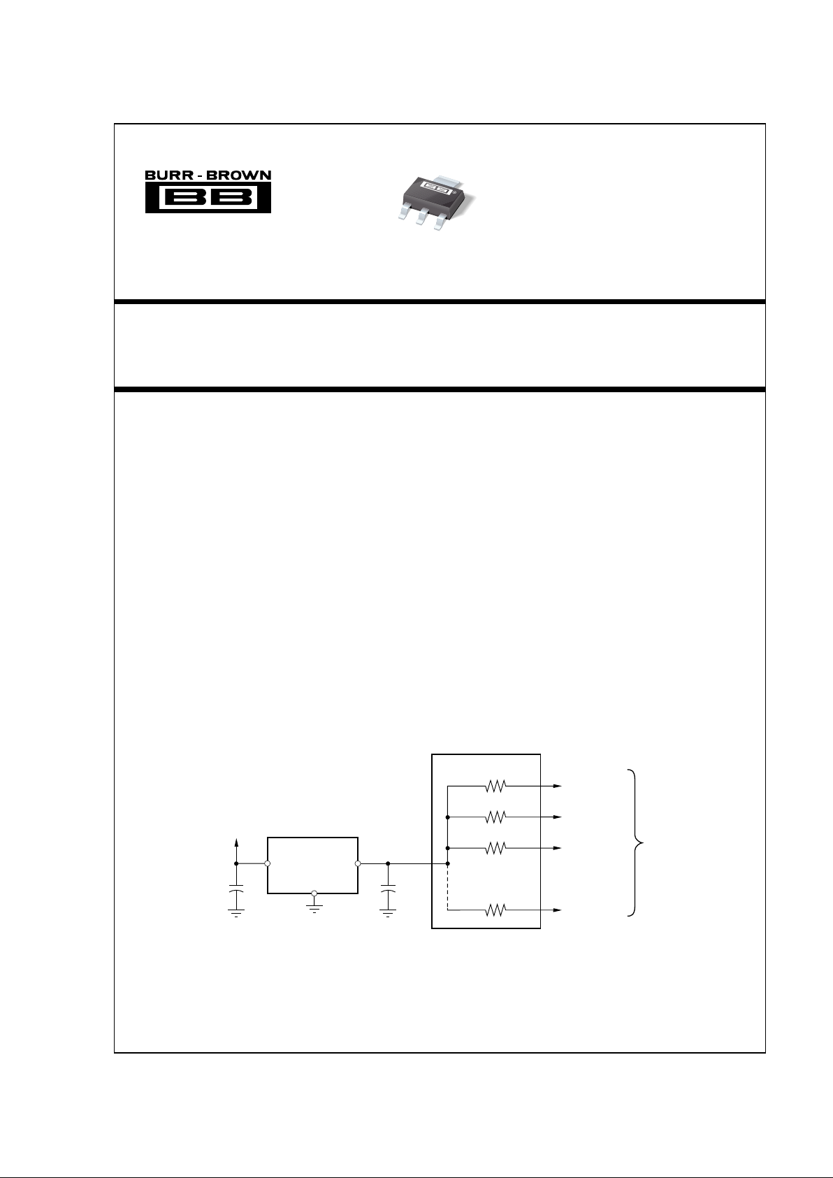
The REG1118-2.85 is a three-terminal voltage regulators capable of sourcing up to 800mA and sinking up
to 400mA. The sinking capability is important in SCSI
applications where active negation line drivers are
used. The REG1118-2.85 is useful for making a
27-line Boulay terminator capable of interfacing with
active negation drivers required in FAST-20 SCSI
applications. The regulator has active current limits
for both sink and source currents as well as internal
thermal limiting.
Laser trimming assures excellent output voltage accuracy. An NPN output stage allows output stage drive
current to contribute to the source load current for
maximum efficiency.
REG1118 is packaged in a SOT-223 surface-mount
package, suitable for reflow soldering techniques.
REG1118
REG1118
GND
V
IN
V
OUT
4.7µF10µF
TERMPWR
110Ω
110Ω
User Supplied
Resistor Network
REG1118-2.85 Used to Make Active Negation SCSI Terminator
Signal Line N
Signal Line 1
Signal Line 2
Signal Line 3
Up To
27 Lines
110Ω
110Ω
®
REG1118
2
SPECIFICATIONS
At TA = 0°C to 70°C, TERMPWR = +5V, unless otherwise noted.
REG1118-2.85
PARAMETER CONDITIONS MIN TYP MAX UNITS
OUTPUT VOLTAGE
No Load, T
A
= 25°C 2.82 2.85 2.88 V
All Operating Conditions
(1)
2.79 2.85 2.91 V
LINE REGULATION
(2)
IO = 0, V
IN
= 4.75V to 6V 0.3 4 mV
LOAD REGULATION
(2)
IO = 0 to 800mA 2 25 mV
I
O
= –400 to 0mA 25 60 mV
DROPOUT VOLTAGE
(3)
TA = 25°C
I
O
= 100mA 0.8 1.1 V
I
O
= 800mA 1.1 1.3 V
CURRENT LIMIT T
A
= 25°C
Positive (I
SC
+)
(4)
800 1450 mA
Negative (I
SC
–) V
OUT
= 3.7V –750 –400 mA
QUIESCENT CURRENT I
O
= 0 3 7 mA
RIPPLE REJECTION T
A
= 25°C
f = 120Hz, V
IN
– V
OUT
= 2V, V
RIPPLE
= 0.5Vp-p 56 dB
LONG-TERM STABILITY
T
A
= +125°C, 1000Hr 0.2 %
THERMAL SHUTDOWN
Junction Temperature Shutdown 150 °C
Junction Temperature Reset 140 °C
THERMAL RESISTANCE
Specified Junction Temperature Range 0 70 °C
Operating Junction Temperature Range 0 125 °C
Storage Range –55 125 °C
Thermal Resistance
θ
JC
(Junction-to-Case at Tab) 15 °C/W
NOTES: (1) All operating conditions include the combined effects of load current, input voltage, and temperature over each parameter’s full specified range.
(2) Load and line regulation are tested at a constant junction temperature by low duty cycle testing. (3) Dropout voltage is defined as the minimum input-to-output
voltage that produces a 1% decrease in output voltage. (4) V
OUT
to ground through 1Ω.
ABSOLUTE MAXIMUM RATINGS
Input Voltage..........................................................................................7V
Output Voltage ........................................................... –0.2V to (V+) +0.5V
Short-Circuit Duration ..................................................................Indefinite
Operating Junction Temperature Range............................. 0°C to +125°C
Storage Temperature Range ..........................................–55°C to +125°C
Lead Temperature (soldering, 10s)
(1)
............................................. +300°C
NOTE: (1) See “Soldering Methods.”
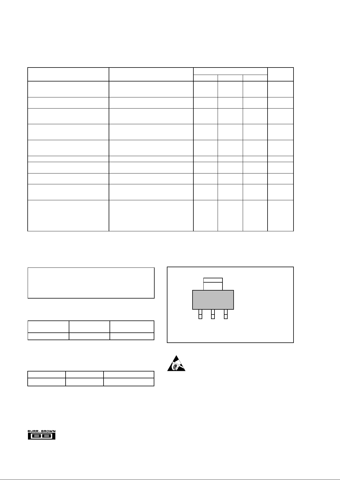
Front View SOT-223
CONNECTION DIAGRAM
Tab is connected
to Ground
V
IN
GroundV
OUT
Plastic SOT-223
PRODUCT
(1)
PART MARKING PACKAGE
REG1118-2.85 BB11182 SOT-223
NOTE: (1) Available in Tape and Reel, add –TR to Model Number.
ORDERING INFORMATION
PACKAGE INFORMATION
PACKAGE DRAWING
PRODUCT PACKAGE NUMBER
(1)
REG1118-2.85 SOT-223 311
NOTE: (1) For detailed drawing and dimension table, please see end of data
sheet, or Appendix C of Burr-Brown IC Data Book.
ELECTROSTATIC
DISCHARGE SENSITIVITY
This integrated circuit can be damaged by ESD. Burr-Brown
recommends that all integrated circuits be handled with
appropriate precautions. Failure to observe proper handling
and installation procedures can cause damage.
 Loading...