

Page 1
Please be aware that an important notice concerning availability, standard warranty, and use in critical applications of Texas Instruments
查询REG1117供应商
800mA and 1A Low Dropout Positive Regulator
1.8V, 2.5V, 2.85, 3.3V, 5V, and Adjustable
REG1117
REG1117A
SBVS001D − OCTOBER 1992 − REVISED JULY 2004
FEATURES
D FIXED AND ADJUSTABLE VERSIONS
D 2.85V MODEL FOR SCSI-2 ACTIVE
TERMINATION
D OUTPUT CURRENT:
REG1117: 800mA max
REG1117A: 1A max
D OUTPUT TOLERANCE: +1% max
D DROPOUT VOLTAGE:
REG1117: 1.2V max at IO = 800mA
REG1117A: 1.3V max at IO = 1A
D INTERNAL CURRENT LIMIT
D THERMAL OVERLOAD PROTECTION
D SOT-223 AND DDPAK SURFACE-MOUNT
PACKAGES
APPLICATIONS
D SCSI-2 ACTIVE TERMINATION
D HAND-HELD DATA COLLECTION DEVICES
D HIGH EFFICIENCY LINEAR REGULATORS
D BATTERY-POWERED INSTRUMENTATION
D BATTERY MANAGEMENT CIRCUITS FOR
NOTEBOOK AND PALMTOP PCs
D CORE VOLTAGE SUPPLY: FPGA, PLD, DSP,
CPU
DESCRIPTION
The REG1117 is a family of easy-to-use three-terminal
voltage regulators. The family includes a variety of fixedand adjustable-voltage versions, two currents (800mA and
1A) and two package types (SOT-223 and DDPAK). See
the chart below for available options.
Output voltage of the adjustable versions is set with two
external resistors. The REG1117 low dropout voltage
allows its use with as little as 1V input-output voltage
differential.
Laser trimming assures excellent output voltage accuracy
without adjustment. An NPN output stage allows output
stage drive to contribute to the load current for maximum
efficiency.
800mA 1A
VOLTAGE SOT-223 DDPAK SOT-223 DDPAK
1.8V n n
2.5V n n
2.85V n
3.3V n n
5V n n
Adjustable n n n
semiconductor products and disclaimers thereto appears at the end of this data sheet.
All trademarks are the property of their respective owners.
! !
www.ti.com
Copyright 1992−2004, Texas Instruments Incorporated
Page 2
"#$$$%
"#$$$%
SBVS001D − OCTOBER 1992 − REVISED JULY 2004
www.ti.com
ABSOLUTE MAXIMUM RATINGS
(1)
Power Dissipation Internally Limited. . . . . . . . . . . . . . . . . . . . . . . . . .
Input Voltage +15V. . . . . . . . . . . . . . . . . . . . . . . . . . . . . . . . . . . . . . .
Operating Junction Temperature Range −40°C to +125°C. . . . . . . .
Storage Temperature Range −65°C to +150°C. . . . . . . . . . . . . . . . .
Lead Temperature (soldering, 10s)
(1)
Stresses above these ratings may cause permanent damage.
(2)
See Soldering Methods section.
(2)
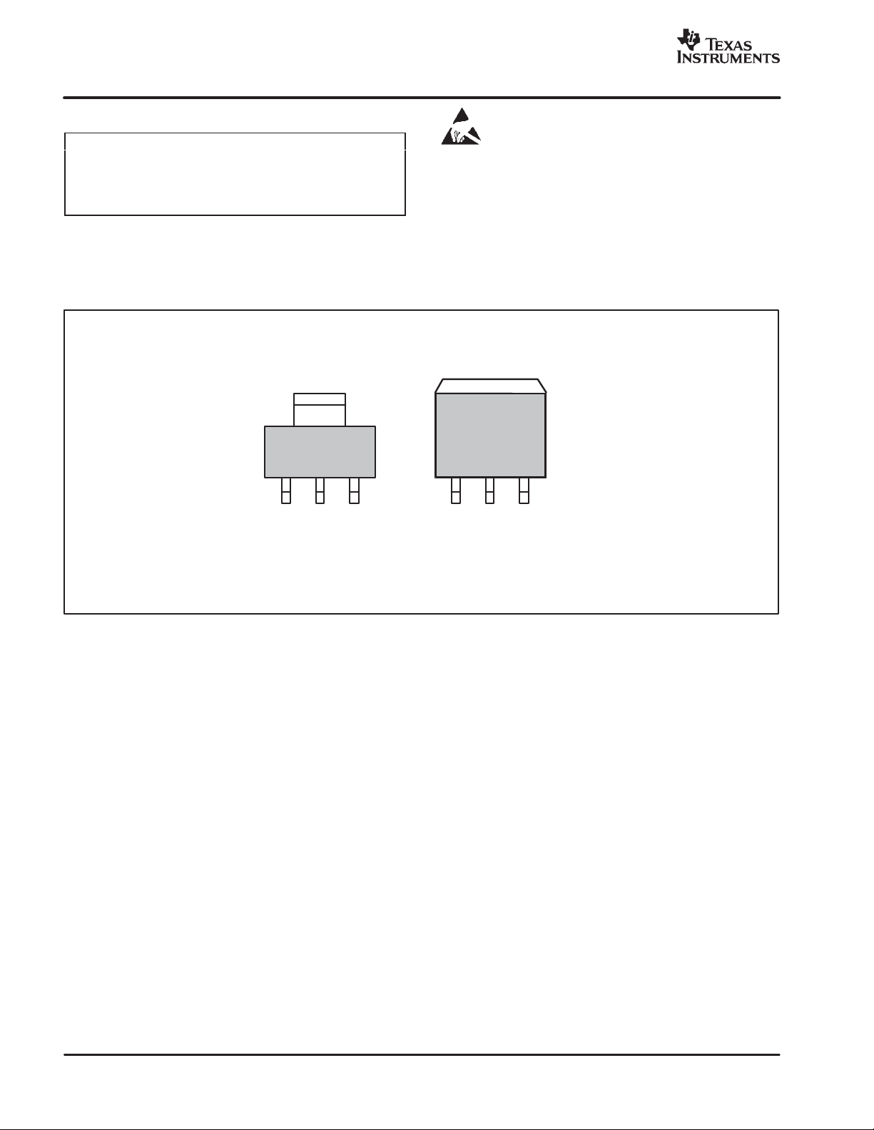
CONNECTION DIAGRAM
Front View
Plastic SOT−223
V
Ground
(Adj.)
OUT
(1)
+300°C. . . . . . . . . . . . . . . . .
Tab isV
V
IN
OUT
This integrated circuit can be damaged by ESD. Texas
Instruments recommends that all integrated circuits be
handled with appropriate precautions. Failure to observe
proper handling and installation procedures can cause damage.
ESD damage can range from subtle performance degradation to
complete device failure. Precision integrated circuits may be more
susceptible t o damage because very small parametric changes could
cause the device not to meet its published specifications.
Plastic DDPAK
Tab is
V
OUT
V
V
Ground
(Adj.)
(1)
OUT
IN
NOTE: (1) Adjustable−Voltage Model.
2
Page 3
www.ti.com
−40°C to
−40 C to
−40°C to
−40 C to
−40°C to
−40 C to
−40°C to
−40 C to
−40°C to
−40 C to
"#$$$%
"#$$$%
SBVS001D − OCTOBER 1992 − REVISED JULY 2004
PACKAGE/ORDERING INFORMATION
PRODUCT VO/I
REG1117-2.85 2.85/800mA SOT223-3 DCY
REG1117-3.3 3.3/800mA SOT223-3 DCY
REG1117F-3.3 3.3/800mA DDPAK-3 KTT
REG1117-5 5V/800mA SOT223-3 DCY
REG1117 Adj./800mA SOT223-3 DCY
REG1117A-1.8 1.8V/1A SOT223-3 DCY
REG11 17F A-1.8 1.8/1A DDPAK-3 KTT
REG1117A-2.5 2.5/1A SOT223-3 DCY
REG11 17F A-2.5 2.5/1A DDPAK-3 KTT
REG1117FA-5 5/1A DDPAK-3 KTT
REG1117A Adj./1A SOT223-3 DCY
REG1117FA Adj./1A DDPAK-3 KTT
(1)
For the most current package and ordering information, see the Package Option Addendum located at the end of this data sheet.
O
PACKAGE-LEAD
(1)
PACKAGE
DESIGNATOR
OPERATING
TEMPERATURE
RANGE
−40°C to
+125°C
−40°C to
+125°C
+125°C
−40°C to
+125°C
−40°C to
+125°C
−40°C to
+125°C
+125°C
−40°C to
+125°C
+125°C
+125°C
−40°C to
+125°C
+125°C
PACKAGE
MARKING
BB11172
BB11174
BB1117F4
BB11175
BB1117
R111718
REG11 17F A1.8
R111725
REG1117FA2.5
BB1117FA5.0
BB1117A
REG1117FA
ORDERING
NUMBER
REG1117-2.85 Rails, 80
REG1117-2.85
REG1117-3.3 Rails, 80
REG1117-3.3
REG1117F-3.3KTTT
REG1117F-3.3/500
REG1117-5 Rails, 80
REG1117-5
REG1117 Rails, 80
REG1117
REG1117A-1.8 Rails, 80
REG1117A-1.8
REG1117FA-1.8KTTT
REG1117FA-1.8/500
REG1117A-2.5 Rails, 80
REG1117A-2.5
REG1117FA-2.5KTTT
REG1117FA-2.5/500
REG1117FA-5/KTTT
REG1117FA-5/500
REG1117A Rails, 80
REG1117A
REG1117FA/KTTT
REG1117FA/500
TRANSPORT
MEDIA,
QUANTITY
T ape and Reel,
2500
T ape and Reel,
2500
T ape and Reel,
50
T ape and Reel,
500
T ape and Reel,
2500
T ape and Reel,
2500
T ape and Reel,
2500
T ape and Reel,
50
T ape and Reel,
500
T ape and Reel,
2500
T ape and Reel,
50
T ape and Reel,
500
T ape and Reel,
50
T ape and Reel,
500
T ape and Reel,
2500
T ape and Reel,
50
T ape and Reel,
500
3
Page 4
"#$$$%
"#$$$%
www.ti.com
SBVS001D − OCTOBER 1992 − REVISED JULY 2004
ELECTRICAL CHARACTERISTICS
At TJ = +25°C, unless otherwise noted.
REG1117, REG1 117A
PARAMETER CONDITION MIN TYP MAX UNIT
OUTPUT VOLTAGE
REG1117-2.85 IO = 10mA, VIN = 4.85V 2.820 2.85 2.880 V
See Note 1 IO = 0 to 800mA, VIN = 4.05V to 10V 2.790 2.85 2.910 V
REG1117-3.3 IO = 10mA, VIN = 5.3V 3.270 3.30 3.330 V
See Note 1 IO = 0 to 800mA, VIN = 4.8V to 10V 3.240 3.30 3.360 V
REG1117-5 IO = 10mA, VIN = 7V 4.950 5.00 5.050 V
See Note 1 IO = 0 to 800mA, VIN = 6.5V to 10V 4.900 5.00 5.100 V
REG1117A-1.8 IO = 10mA, VIN = 3.8V 1.782 1.8 1.818 V
See Note 1 IO = 0 to 1A, VIN = 3.8V to 10V 1.764 1.8 1.836 V
REG1117A-2.5 IO = 10mA, VIN = 4.5V 2.475 2.5 2.525 V
See Note 1 IO = 0 to 1A, VIN = 4.5V to 10V 2.450 2.5 2.550 V
REG1117A-5 IO = 10mA, VIN = 7V 4.950 5.0 5.050 V
See Note 1 IO = 0 to 1A, VIN = 7V to 10V 4.900 5.0 5.100 V
REFERENCE VOLTAGE
REG1117 (Adjustable) IO = 10mA, VIN − VO = 2V 1.238 1.250 1.262 V
See Note 1 IO = 10 to 800mA, VIN − VO = 1.4 to 10V 1.225 1.250 1.280 V
REG1117A (Adjustable) IO = 10mA, VIN − VO = 2V 1.238 1.250 1.262 V
See Note 1 IO = 10mA to 1A, VIN − VO = 1.4 to 10V 1.225 1.250 1.280 V
LINE REGULATION
(1)
(1)
(1)
(1)
(1)
(1)
(1)
(1)
(1)
(1)
(1)
(1)
(1)
(1)
(1)(2)
(1)(2)
(3)
IO = 0, VIN = 4.25 to 10V 1 7 mV
IO = 0, VIN = 4.8 to 10V 2 7 mV
IO = 0, VIN = 6.5 to 15V 3 10 mV
IO = 10mA, VIN − VO = 1.5 to 13.75V 0.1 0.4 %
IO = 10mA, VIN − VO = 1.5 to 13.75V 0.1 0.4 %
IO = 0, VIN = 3.8V to 10V 1 7 mV
IO = 0, VIN = 4.5V to 10V 1 7 mV
IO = 0, VIN = 7V to 15V 3 10 mV
IO = 0 to 800mA, VIN = 4.25V 2 10 mV
IO = 0 to 800mA, VIN = 4.8V 3 12 mV
IO = 0 to 800mA, VIN = 6.5V 3 15 mV
IO = 10 to 800mA, VIN − VO = 3V 0.1 0.4 %
IO = 10mA to 1A, VIN − VO = 3V 0.1 0.4 %
IO = 0 to 1A, VIN = 3.8V 2 10 mV
IO = 100mA 1.00 1.10 V
IO = 800mA 1.10 1.20 V
REG1117-2.85
REG1117-3.3
REG1117-5
REG1117 (Adjustable)
REG1117A (Adjustable)
REG1117A-1.8
REG1117A-2.5
REG1117A-5.0
LOAD REGULATION
REG1117-2.85
REG1117-3.3
REG1117-5
REG1117 (Adjustable)
REG1117A (Adjustable)
REG1117A-1.8
REG1117A-2.5 IO = 0 to 1A, VIN = 4.5V 2 10 mV
REG1117A-5 IO = 0 to 1A, VIN = 7.0V 3 15 mV
DROPOUT VOLTAGE
All Models
See Note 1 IO = 500mA 1.05 1.15 V
REG1117 Models
REG1117A IO = 1A 1.2 1.30 V
See Note 1 IO = 1A 1.2 1.55 V
(1)
Specification applies over the full specified junction temperature range, 0°C to +125°C.
(2)
REG1117 and REG1117A adjustable versions require a minimum load current for ±3% regulation.
(3)
Dropout voltage is the input voltage minus output voltage that produces a 1% decrease in output voltage.
(4)
Percentage change in unloaded output voltage before versus after a 30ms power pulse of IO = 800mA (REG11 17 models), IO = 1A (REG11 17A),
VIN − VO = 1.4V (reading taken 10ms after pulse).
4
Page 5
"#$$$%
"#$$$%
www.ti.com
SBVS001D − OCTOBER 1992 − REVISED JULY 2004
ELECTRICAL CHARACTERISTICS (continued)
At TJ = +25°C, unless otherwise noted.
REG1117, REG1 117A
PARAMETER UNITMAXTYPMINCONDITION
CURRENT LIMIT
REG1117 Models VIN − VO = 5V 800 950 1200 mA
REG1117A VIN − VO = 5V 1000 1250 1600 mA
MINIMUM LOAD CURRENT
(4)
(1)(2)
(1)
JC
JA
(1)
(1)(2)
(1)
VIN − VO = 13.75V 1.7 5 mA
VIN − VO = 5V 4 10 mA
IO = 10mA, VIN − VO = 1.4 to 10V 50 120 µA
IO = 10mA to 800mA, VIN − VO = 1.4 to 10V 0.5 5 µA
IO = 10mA to 1A, VIN − VO = 1.4 to 10V 0.5 5 µA
30ms Pulse 0.01 0.1 %/W
= 3V + 1VPP Ripple 62 dB
OUT
(Junction-to-Case at Tab)
dc 3 °C/W
(Junction-to-Case at Tab)
Adjustable Models
QUIESCENT CURRENT
Fixed-Voltage Models
ADJUSTABLE PIN CURRENT
vs Load Current, REG1117
vs Load Current, REG1117A
THERMAL REGULATION
All Models
RIPPLE REJECTION
All Models f = 120Hz, VIN − V
TEMPERATURE DRIFT
Fixed-Voltage Models TJ = 0°C to +125°C 0.5 %
Adjustable Models TJ = 0°C to +125°C 2 %
LONG-TERM STABILITY
All Models TA = 125°C, 1000Hr 0.3 %
OUTPUT NOISE
rms Noise, All Models f = 10Hz to 10kHz 0.003 %
THERMAL RESISTANCE
Thermal Resistance, q
3-Lead SOT-223 Surface-Mount 15 °C/W
3-Lead DDPAK Surface-Mount f > 50Hz 2 °C/W
Thermal Resistance, q
3-Lead DDPAK Surface-Mount No Heatsink 65 °C/W
(1)
Specification applies over the full specified junction temperature range, 0°C to +125°C.
(2)
REG1117 and REG1117A adjustable versions require a minimum load current for ±3% regulation.
(3)
Dropout voltage is the input voltage minus output voltage that produces a 1% decrease in output voltage.
(4)
Percentage change in unloaded output voltage before versus after a 30ms power pulse of IO = 800mA (REG11 17 models), IO = 1A (REG11 17A),
VIN − VO = 1.4V (reading taken 10ms after pulse).
5
Page 6

"#$$$%
"#$$$%
SBVS001D − OCTOBER 1992 − REVISED JULY 2004
SIMPLIFIED SCHEMATIC
Thermal
Limit
Current
Limit
www.ti.com
V
IN
+
10X
Ground (Fixed−voltage Models)
Adj.(Adjustable−voltage Model)
(Substrate)
V
OUT
6
Page 7

www.ti.com
TYPICAL CHARACTERISTICS
At TA = +25°C, all models, unless otherwise noted.
SHORT−CIRCUIT CURRENT vsTEMPERATURE
REG1117A
REG1117 Models
−
−
50
25 0 25 50 75 100
Temperature (_C)
Short−Circuit Current(mA)
1400
1300
1200
1100
1000
900
800
"#$$$%
"#$$$%
SBVS001D − OCTOBER 1992 − REVISED JULY 2004
LOAD REGULATION
(∆
= 800mA)
I
1
0
1
−
2
−
3
−
4
−
5
Output Voltage Deviation (mV)
−
6
−
7
−
50
−
25 0 25 50 75 100
LOAD
REG1117−2.85
REG1117A−1.8
REG1117−5
Temperature(_C)
6
5
4
3
2
1
0
Output Voltage Change (mV)
−
1
−
2
−
50
2.0
1.0
0
−
1.0
Output Voltage Change (%)
−
2.0
−
LINE REGULATION vsTEMPERATURE
VIN=6.5Vto15V
REG1117−5
REG1117A−1.8
=3.8Vto10V
V
IN
−
25 0 25 50 75 100
Temperature (_C)
OUTPUT VOLTAGE vs TEMPERATURE
−
50
25 0 25 50 75 100
Temperature (_C)
IO=10mA
100
90
80
70
60
50
40
30
Ripple Rejection (dB)
20
10
0
10 100 1k 10k 100k
8
7
6
5
4
3
2
Quiescent Current (mA)
1
0
−
50
RIPPLE REJECTION vs FREQUENCY
I
=100mA
OUT
=1.0V
V
RIPPLE
Frequency (Hz)
QUIESCENT CURRENT vs TEMPERATURE
Fixed−Voltage Models
−
25 0 25 50 75 100
Temperature (_C)
PP
7
Page 8

"#$$$%
"#$$$%
SBVS001D − OCTOBER 1992 − REVISED JULY 2004
TYPICAL CHARACTERISTICS (continued)
At TA = +25°C, all models, unless otherwise noted.
www.ti.com
LOAD TRANSIENT RESPONSE
0.1
0
0.1
−
Deviations (V)
Output Voltage
=10µF
C
0.5
0
0.5
−
Load Current (A)
0 20406080100
Time (µs)
IN
C
=10µF
OUT
Tantalum
V
=4.25V
IN
Preload =0.1A
APPLICATIONS INFORMATION
Figure 1 shows the basic hookup diagram for fixed-voltage
models. All models require an output capacitor for proper
operation, and for improving high-frequency load
regulation; a 10µF tantalum capacitor is recommended.
Aluminum electrolytic types of 50µF or greater can also be
used. A high-quality capacitor should be used to assure
that the ESR (Effective Series Resistance) is less than
0.5Ω.
V
IN
10µF
Tantalum
REG1117
++
10µF
Tantalum
V
O
60
40
20
0
Deviation (mV)
Output Voltage
20
−
40
−
5.25
4.25
3.25
Input Voltage (V)
0 20 40 60 80 100 120 140 160 180 200
LINE TRANSIENTRESPONSE
CIN=1µF
C
=10µFTantalum
OUT
I
=0.1A
OUT
Time (µs)
Figure 2 shows a hookup diagram for the adjustable
voltage model. Resistor values are shown for some
commonly-used output voltages. V alues for other voltages
can be calculated from the equation shown in Figure 2. For
best load regulation, connect R
close to the ground side of the load as shown.
R
2
close to the output pin and
1
THERMAL CONSIDERATIONS
The REG1117 has current limit and thermal shutdown
circuits that protect it from overload. The thermal shutdown
activates at approximately T
operation, however, the junction temperature should not
be allowed to exceed 125°C. Any tendency to activate the
thermal shutdown in normal use is an indication of an
inadequate heat sink or exc e s s i v e power dissipation. The
power dissipation is equal to:
PD = (VIN – V
OUT
) I
The junction temperature can be calculated by:
= 165°C. For continuous
J
OUT
Figure 1. Fixed-Voltage Model—Basic
Connections
V
IN
10µF
NOTES: (1) C
32
REG1117
C
+
1
(Adj)
1
(1)
C
+
3
10µF
optional. Improves high−frequency line rejection. (2) Resistors are standard 1% values.
3
Figure 2. Adjustable-Voltage Model—Basic Connections
8
TJ = TA + PD (qJA)
where TA is the ambient temperature, and qJA is the
junction-to-ambient thermal resistance.
V
O
C
+
2
R
10µF
1
Load
R
2
R1+R
V
O
2
= x (1.25V) + (50µA) (R2)
R
1
This term is negligible with
proper choice of values−see
table at right.
V
OUT
(V)(Ω)
1.25 Open Short
1.5 750 147
2.1 158 107
2.85 169 215
3 137 191
3.3 115 187
5 113 340
10 113 787
R
1
(2)
R
(Ω)
2
(2)
Page 9

www.ti.com
"#$$$%
"#$$$%
SBVS001D − OCTOBER 1992 − REVISED JULY 2004
A simple experiment will determine whether the maximum
recommended junction temperature is exceeded in an
actual circuit board and mounting configuration: Increase
the ambient temperature above that expected in normal
operation until the device’s thermal shutdown is activated.
If this occurs at more than 40°C above the maximum
expected ambient temperature, then T
will be less than
J
125°C during normal operation.
The internal protection circuitry of the REG1117 was
designed to protect against overload conditions. It was not
intended to replace proper heat sinking. Continuously
running the REG1117 into thermal shutdown will degrade
reliability.
0.45
LAYOUT CONSIDERATIONS
The DDPAK (REG1117F-3.3 and REG1117FA) is a
surface-mount power package that has excellent thermal
characteristics. For best thermal performance, the
mounting tab should be soldered directly to a circuit board
copper area, as shown in Figure 3. Increasing the copper
area improves heat dissipation. Figure 4 shows typical
thermal resistance from junction-to-ambient as a function
of the copper area.
3−Lead DDPAK
0.51
(1)
0.085
All measurements
in inches.
0.155 0.05
NOTE: (1) For improved thermal performance increase
footprint area. See Figure 4 (Thermal Resistance vs
Circuit Board Copper Area).
Figure 3. DDPAK Footprint
THERMAL RESISTANCE vs
60
50
(°C/W)
JA
40
30
20
Thermal Resistance, q
10
012345
CIRCUIT BOARD COPPER AREA
DDPAK Surface Mount Package
Copper Area (inches
REG1117F
1oz copper
2
)
0.2
0.10
Circuit Board CopperArea
REG1117F
DDPAK Surface−Mount Package
Figure 4. DDPAK Thermal Resistance versus Circuit Board Copper Area
9
Page 10

"#$$$%
(1)
THERMAL
BOARD
COPPER
COPPER
JUNCTION-
"#$$$%
SBVS001D − OCTOBER 1992 − REVISED JULY 2004
www.ti.com
The SOT-223 package derives heat sinking from
conduction through its copper leads, especially the large
mounting tab. These must be soldered to a circuit board
with a substantial amount of copper remaining, as shown
in Figure 5. Circuit board traces connecting the tab and the
leads should be made as large as practical. The mounting
tab of both packages is electrically connected to V
Total Area: 50 x 50mm
35 x 17mm
16 x 10 mm 16 x 10 mm
q
≈59_
Without backside copper:
With solid backside copper:
q
JA
JA
≈49_
C/W
C/W
OUT
.
Figure 5. SOT-223 Circuit Board Layout Example
Other nearby circuit traces, including those on the back
side of the circuit board, help conduct heat away from the
device, even though they may not be electrically
connected. Make all nearby copper traces as wide as
possible and leave only narrow gaps between traces.
Table 1 shows approximate values of q
for various circuit
JA
board and copper areas for the SOT-223 package. Nearby
heat dissipating components, circuit board mounting
conditions, and ventilation can dramatically affect the
actual q
. Proper heat sinking significantly increases the
JA
maximum power dissipation at a given ambient
temperature, as shown in Figure 6.
Table 1. SOT-223 qJA for Various Board
Configurations
SOT-223
TOTAL PC
AREA
2500mm
2500mm
2500mm
2500mm
2500mm
1600mm
2500mm
2500mm
1600mm
900mm
900mm
(1)
Tab is attached to the topside copper.
TOPSIDE
AREA
2
2500mm
2
1250mm
2
2
2
2
2
2
2
2
2
950mm
2500mm
1800mm
600mm
1250mm
915mm
600mm
340mm
340mm
2
2
2
2
2
2
2
2
2
2
2
BACKSIDE
AREA
2500mm
2500mm
2500mm
2
2
2
0 51°C/W
0 53°C/W
1600mm
2
0 58°C/W
0 59°C/W
0 67°C/W
2
900mm
0 85°C/W
RESISTANCE
TO-AMBIENT
46°C/W
47°C/W
49°C/W
55°C/W
72°C/W
SOLDERING METHODS
Both REG1117 packages are suitable for infrared reflow
and vapor-phase reflow soldering techniques. The high
rate of temperature change that occurs with wave
soldering or hand soldering can damage the REG1117.
INSPEC Abstract Number: B91007604, C91012627.
Kelly, E.G. “Thermal Characteristics of Surface 5WK9Ω
Packages.” The Proceedings of SMTCON
Technology Conference and Exposition: Competitive
Surface Mount Technology, April 3−6, 1990, Atlantic City,
NJ, USA. Abstract Publisher: IC Manage, 1990, Chicago,
IL, USA.
. Surface Mount
10
MAXIMUM POWER DISSIPATION
6
5
=46_C/W
q
4
JA
(2500mm2topside and
backside copper)
3
q
=65_C/W
JA
2
Power Dissipation (Watts)
q
JA
1
(340mm2topside copper,
no backside copper)
0
0 255075100125
vs AMBIENT TEMPERATURE
=27_C/W
q
JA
(4in2one ozcopper
mounting pad)
(no heatsink)
=85_C/W
Ambient Temperature (_C)
PD=(TJ(max)−TA)/
TJ(max) =150_C
DDPAK
SOT−223
q
JA
Figure 6. Maximum Power Dissipation versus Ambient Temperature
Page 11

www.ti.com
"#$$$%
"#$$$%
SBVS001D − OCTOBER 1992 − REVISED JULY 2004
5V
TERMPWR
Ω
1N5817
REG1117−2.85
2.85V 2.85V
10µF10µF
110
110
(Upto27Lines)
Ω
Figure 7. SCSI Active Termination Configuration
REG1117−5
VIN> 12V
10µF100
In Out
++
10µF
GND
+
Ω
1k
5V to 10V
µ
F
TERMPWR
Ω
110
Ω
110
++
10µF100
REG1117−2.85
10µF 10µF
REG1117−5
In Out
GND
2.5V
REF1004−2.5
OUT
1N5817
5V
7.5VVIN>9.0V
µ
F
Figure 8. Adjusting Output of Fixed Voltage Models
V
IN
+
10µF
Ω
1k
6.5V
++
10µF
Figure 10. Battery Backed-Up Regulated Supply
V
IN
10µF 100µF
Figure 9. Regulator with Reference
REG1117−5
In Out
GND
Ω
50
REG1117−5
In Out
GND
REG1117−5
In Out
++
GND
5.2V Line
5.0V Battery
100µF
Floating Input
Figure 11. Low Dropout Negative Supply
V
=−5V
OUT
11
Page 12

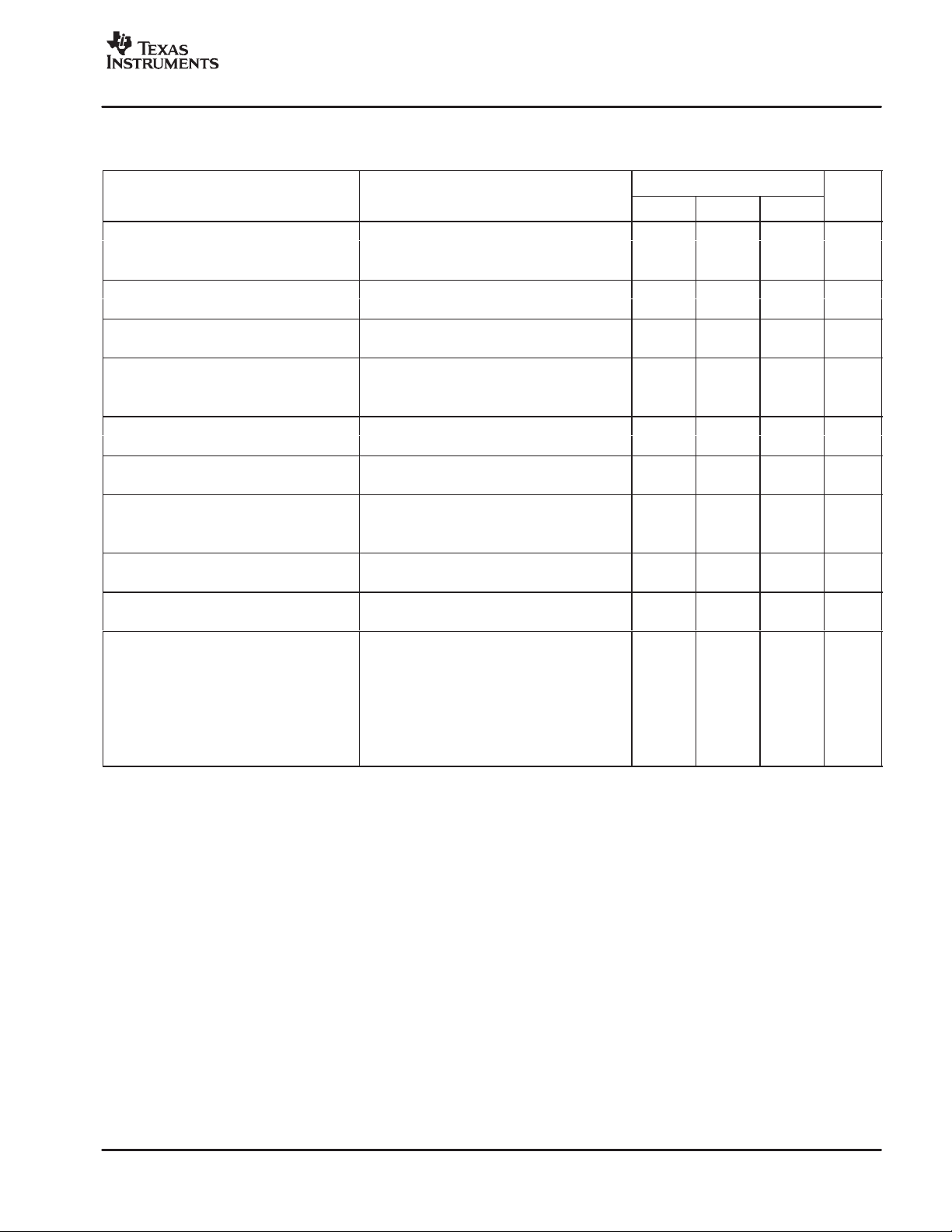
PACKAGE OPTION ADDENDUM
www.ti.com
PACKAGING INFORMATION
Orderable Device Status
REG1117 ACTIVE SOT-223 DCY 4 80 TBD CU SNPB Level-3-220C-168 HR
REG1117-2.85 ACTIVE SOT-223 DCY 4 80 TBD CU SNPB Level-3-220C-168 HR
REG1117-2.85/2K5 ACTIVE SOT-223 DCY 4 2500 TBD CU SNPB Level-3-220C-168HR
REG1117-3.3 ACTIVE SOT-223 DCY 4 80 TBD CU SNPB Level-3-220C-168 HR
REG1117-3.3/2K5 ACTIVE SOT-223 DCY 4 2500 TBD CU SNPB Level-3-220C-168 HR
REG1117-5 ACTIVE SOT-223 DCY 4 80 TBD CU SNPB Level-3-220C-168 HR
REG1117-5/2K5 ACTIVE SOT-223 DCY 4 2500 TBD CU SNPB Level-3-220C-168 HR
REG1117/2K5 ACTIVE SOT-223 DCY 4 2500 TBD CU SNPB Level-3-220C-168 HR
REG1117A ACTIVE SOT-223 DCY 4 80 TBD CU SNPB Level-3-220C-168 HR
REG1117A-1.8 ACTIVE SOT-223 DCY 4 80 TBD CU SNPB Level-3-220C-168 HR
REG1117A-1.8/2K5 ACTIVE SOT-223 DCY 4 2500 TBD CU SNPB Level-3-220C-168HR
REG1117A-2.5 ACTIVE SOT-223 DCY 4 80 TBD CU SNPB Level-3-220C-168 HR
REG1117A-2.5/2K5 ACTIVE SOT-223 DCY 4 2500 TBD CU SNPB Level-3-220C-168HR
REG1117A/2K5 ACTIVE SOT-223 DCY 4 2500 TBD CU SNPB Level-3-220C-168 HR
REG1117F-3.3 OBSOLETE DDPAK/
REG1117F-3.3/500 ACTIVE DDPAK/
REG1117F-3.3KTTT ACTIVE DDPAK/
REG1117FA OBSOLETE DDPAK/
REG1117FA-1.8 OBSOLETE DDPAK/
REG1117FA-1.8/500 ACTIVE DDPAK/
REG1117FA-1.8KTTT ACTIVE DDPAK/
REG1117FA-2.5 OBSOLETE DDPAK/
REG1117FA-2.5/500 ACTIVE DDPAK/
REG1117FA-2.5KTTT ACTIVE DDPAK/
REG1117FA-5.0 OBSOLETE DDPAK/
REG1117FA-5.0/500 ACTIVE DDPAK/
REG1117FA-5.0KTTT ACTIVE DDPAK/
REG1117FA/500 ACTIVE DDPAK/
REG1117FA2.5KTTTG3 ACTIVE DDPAK/
REG1117FAKTTT ACTIVE DDPAK/
(1)
Package
Type
TO-263
TO-263
TO-263
TO-263
TO-263
TO-263
TO-263
TO-263
TO-263
TO-263
TO-263
TO-263
TO-263
TO-263
TO-263
TO-263
Package
Drawing
KTT 3 TBD CallTI Call TI
KTT 3 500 Green (RoHS &
KTT 3 50 Green (RoHS &
KTT 3 TBD CallTI Call TI
KTT 3 TBD CallTI Call TI
KTT 3 500 Green (RoHS &
KTT 3 50 Green (RoHS &
KTT 3 TBD CallTI Call TI
KTT 3 500 Green (RoHS &
KTT 3 50 Green (RoHS &
KTT 3 TBD CallTI Call TI
KTT 3 500 TBD CU SN Level-3-235C-168HR
KTT 3 50 TBD CU SN Level-3-235C-168HR
KTT 3 500 Green (RoHS &
KTT 3 50 Green (RoHS &
KTT 3 50 Green (RoHS &
Pins Package
Qty
Eco Plan
no Sb/Br)
no Sb/Br)
no Sb/Br)
no Sb/Br)
no Sb/Br)
no Sb/Br)
no Sb/Br)
no Sb/Br)
no Sb/Br)
(2)
Lead/Ball Finish MSL Peak Temp
CU SN Level-2-260C-1 YEAR
CU SN Level-2-260C-1 YEAR
CU SN Level-2-260C-1 YEAR
CU SN Level-2-260C-1 YEAR
CU SN Level-2-260C-1 YEAR
CU SN Level-2-260C-1 YEAR
CU SN Level-2-260C-1 YEAR
CU SN Level-2-260C-1 YEAR
CU SN Level-2-260C-1 YEAR
27-Sep-2005
(3)
Addendum-Page 1
Page 13

PACKAGE OPTION ADDENDUM
www.ti.com
(1)
The marketing status values are defined as follows:
27-Sep-2005
ACTIVE: Product device recommended for new designs.
LIFEBUY: TI has announced that the device will be discontinued, and a lifetime-buy period is in effect.
NRND: Not recommended for new designs. Device is in production to support existing customers, but TI does not recommend using this part in
a new design.
PREVIEW: Device has been announced but is not in production. Samples may or may not be available.
OBSOLETE: TI has discontinued the production of the device.
(2)
Eco Plan - The planned eco-friendly classification: Pb-Free (RoHS) or Green (RoHS & no Sb/Br) - please check
http://www.ti.com/productcontent for the latest availability information and additional product content details.
TBD: The Pb-Free/Green conversion plan has not been defined.
Pb-Free (RoHS): TI's terms "Lead-Free" or "Pb-Free" mean semiconductor products that are compatible with the current RoHS requirements
for all 6 substances, including the requirement that lead not exceed 0.1% by weight in homogeneous materials. Where designed to be soldered
at high temperatures, TI Pb-Free products are suitable for use in specified lead-free processes.
Green (RoHS & no Sb/Br): TI defines "Green" to mean Pb-Free (RoHS compatible), and free of Bromine (Br) and Antimony (Sb) based flame
retardants (Br or Sb do not exceed 0.1% by weight in homogeneous material)
(3)
MSL, Peak Temp. -- The Moisture Sensitivity Level rating according to the JEDEC industry standard classifications, and peak solder
temperature.
Important Information and Disclaimer:The information provided on this page represents TI's knowledge and belief as of the date that it is
provided. TI bases its knowledge and belief on information provided by third parties, and makes no representation or warranty as to the
accuracy of such information. Efforts are underway to better integrate information from third parties. TI has taken and continues to take
reasonable steps to provide representative and accurate information but may not have conducted destructive testing or chemical analysis on
incoming materials and chemicals. TI and TI suppliers consider certain information to be proprietary, and thus CAS numbers and other limited
information may not be available for release.
In no event shall TI's liability arising out of such information exceed the total purchase price of the TI part(s) at issue in this document sold by TI
to Customer on an annual basis.
Addendum-Page 2
Page 14

MECHANICAL DATA
MPDS094A – APRIL 2001 – REVISED JUNE 2002
DCY (R-PDSO-G4) PLASTIC SMALL-OUTLINE
6,70 (0.264)
6,30 (0.248)
3,10 (0.122)
4
2,90 (0.114)
0,10 (0.004)
M
7,30 (0.287)
6,70 (0.264)
1 2 3
2,30 (0.091)
4,60 (0.181)
1,80 (0.071) MAX
0,10 (0.0040)
0,02 (0.0008)
NOTES: A. All linear dimensions are in millimeters (inches).
B. This drawing is subject to change without notice.
C. Body dimensions do not include mold flash or protrusion.
D. Falls within JEDEC TO-261 Variation AA.
3,70 (0.146)
3,30 (0.130)
0,84 (0.033)
0,66 (0.026)
0,10 (0.004)
1,70 (0.067)
1,50 (0.059)
Seating Plane
M
0,08 (0.003)
0°–10°
Gauge Plane
0,25 (0.010)
0,75 (0.030) MIN
0,35 (0.014)
0,23 (0.009)
4202506/B 06/2002
POST OFFICE BOX 655303 • DALLAS, TEXAS 75265
Page 15

Page 16

IMPORTANT NOTICE
Texas Instruments Incorporated and its subsidiaries (TI) reserve the right to make corrections, modifications,
enhancements, improvements, and other changes to its products and services at any time and to discontinue
any product or service without notice. Customers should obtain the latest relevant information before placing
orders and should verify that such information is current and complete. All products are sold subject to TI’s terms
and conditions of sale supplied at the time of order acknowledgment.
TI warrants performance of its hardware products to the specifications applicable at the time of sale in
accordance with TI’s standard warranty. Testing and other quality control techniques are used to the extent TI
deems necessary to support this warranty . Except where mandated by government requirements, testing of all
parameters of each product is not necessarily performed.
TI assumes no liability for applications assistance or customer product design. Customers are responsible for
their products and applications using TI components. To minimize the risks associated with customer products
and applications, customers should provide adequate design and operating safeguards.
TI does not warrant or represent that any license, either express or implied, is granted under any TI patent right,
copyright, mask work right, or other TI intellectual property right relating to any combination, machine, or process
in which TI products or services are used. Information published by TI regarding third-party products or services
does not constitute a license from TI to use such products or services or a warranty or endorsement thereof.
Use of such information may require a license from a third party under the patents or other intellectual property
of the third party, or a license from TI under the patents or other intellectual property of TI.
Reproduction of information in TI data books or data sheets is permissible only if reproduction is without
alteration and is accompanied by all associated warranties, conditions, limitations, and notices. Reproduction
of this information with alteration is an unfair and deceptive business practice. TI is not responsible or liable for
such altered documentation.
Resale of TI products or services with statements different from or beyond the parameters stated by TI for that
product or service voids all express and any implied warranties for the associated TI product or service and
is an unfair and deceptive business practice. TI is not responsible or liable for any such statements.
Following are URLs where you can obtain information on other Texas Instruments products and application
solutions:
Products Applications
Amplifiers amplifier.ti.com Audio www.ti.com/audio
Data Converters dataconverter.ti.com Automotive www.ti.com/automotive
DSP dsp.ti.com Broadband www.ti.com/broadband
Interface interface.ti.com Digital Control www.ti.com/digitalcontrol
Logic logic.ti.com Military www.ti.com/military
Power Mgmt power.ti.com Optical Networking www.ti.com/opticalnetwork
Microcontrollers microcontroller.ti.com Security www.ti.com/security
Telephony www.ti.com/telephony
Video & Imaging www.ti.com/video
Wireless www.ti.com/wireless
Mailing Address: Texas Instruments
Post Office Box 655303 Dallas, Texas 75265
Copyright 2005, Texas Instruments Incorporated
 Loading...